EP0706257A2 - Circuit d'alimentation à découpage - Google Patents
Circuit d'alimentation à découpage Download PDFInfo
- Publication number
- EP0706257A2 EP0706257A2 EP95115018A EP95115018A EP0706257A2 EP 0706257 A2 EP0706257 A2 EP 0706257A2 EP 95115018 A EP95115018 A EP 95115018A EP 95115018 A EP95115018 A EP 95115018A EP 0706257 A2 EP0706257 A2 EP 0706257A2
- Authority
- EP
- European Patent Office
- Prior art keywords
- base current
- capacitor
- voltage
- current
- primary winding
- Prior art date
- Legal status (The legal status is an assumption and is not a legal conclusion. Google has not performed a legal analysis and makes no representation as to the accuracy of the status listed.)
- Withdrawn
Links
- 239000003990 capacitor Substances 0.000 claims abstract description 24
- 238000004804 winding Methods 0.000 claims abstract description 17
- 102100037460 E3 ubiquitin-protein ligase Topors Human genes 0.000 abstract description 3
- 101000662670 Homo sapiens E3 ubiquitin-protein ligase Topors Proteins 0.000 abstract description 3
- 101000610551 Homo sapiens Prominin-1 Proteins 0.000 abstract description 3
- 102100040120 Prominin-1 Human genes 0.000 abstract description 3
- 101000717877 Saccharomyces cerevisiae (strain ATCC 204508 / S288c) 40S ribosomal protein S11-A Proteins 0.000 abstract description 3
- 101000717881 Saccharomyces cerevisiae (strain ATCC 204508 / S288c) 40S ribosomal protein S11-B Proteins 0.000 abstract description 3
- 238000005457 optimization Methods 0.000 abstract 1
- 230000001419 dependent effect Effects 0.000 description 3
- 101100440894 Arabidopsis thaliana CP33 gene Proteins 0.000 description 1
- 238000010586 diagram Methods 0.000 description 1
- 238000009499 grossing Methods 0.000 description 1
- 230000001939 inductive effect Effects 0.000 description 1
Images
Classifications
-
- H—ELECTRICITY
- H02—GENERATION; CONVERSION OR DISTRIBUTION OF ELECTRIC POWER
- H02M—APPARATUS FOR CONVERSION BETWEEN AC AND AC, BETWEEN AC AND DC, OR BETWEEN DC AND DC, AND FOR USE WITH MAINS OR SIMILAR POWER SUPPLY SYSTEMS; CONVERSION OF DC OR AC INPUT POWER INTO SURGE OUTPUT POWER; CONTROL OR REGULATION THEREOF
- H02M3/00—Conversion of DC power input into DC power output
- H02M3/22—Conversion of DC power input into DC power output with intermediate conversion into AC
- H02M3/24—Conversion of DC power input into DC power output with intermediate conversion into AC by static converters
- H02M3/28—Conversion of DC power input into DC power output with intermediate conversion into AC by static converters using discharge tubes with control electrode or semiconductor devices with control electrode to produce the intermediate AC
- H02M3/325—Conversion of DC power input into DC power output with intermediate conversion into AC by static converters using discharge tubes with control electrode or semiconductor devices with control electrode to produce the intermediate AC using devices of a triode or a transistor type requiring continuous application of a control signal
- H02M3/335—Conversion of DC power input into DC power output with intermediate conversion into AC by static converters using discharge tubes with control electrode or semiconductor devices with control electrode to produce the intermediate AC using devices of a triode or a transistor type requiring continuous application of a control signal using semiconductor devices only
Definitions
- the invention relates to a switch mode power supply circuit (SMPS) according to the introductory part of claim 1.
- SMPS switch mode power supply circuit
- a driver stage especially in push/pull relationship for providing a base current for the switching transistor being connected via a primary winding of the transformer to a DC operating voltage.
- the supply terminal of said driver stage is connected to a charging capacitor which is connected to a current source preferably being connected to the main rectifier.
- base current is derived from said charging capacitor via said driver stage to base of said switching transistor.
- the supply terminal of the driver stage which is connected to said charging capacitor is additionally connected to the output of a rectifier having its input connected to a primary winding of the SMPS-transformer.
- Said rectifier provides an additional current source for the charging capacitor and the driver stage. Thereby an undesired under-voltage at said capacitor during start-up can be reduced or even be avoided.
- said rectifier is supplied by said primary winding of said transformer which is connected to operating potential derived from main voltage said additional charging current for said charging capacitor advantageously is dependent from main voltage. If main voltage increases and drive base current for said switching transistor should be increased, too, said additional charging current for said charging capacitor is also increased. That means that an optimizing the driving capability independent from main fluctuation is achieved.
- the invention only needs a few additional elements so that additional costs for the switch mode power supply remain very low.
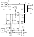
- main voltage UN main rectifier BR, smoothing capacitor C1, transformer Tr having main primary winding W1, secondary winding W2 and an additional winding W3, switching transistor TP10, control circuit C, driver stage TP01, biasing network including Zener diode DP33 and capacitor CP33, charging capacitor CP04 connected to current source CS and via resistor RP41 to supply terminal a of driver stage TP01.
- TP10 is switched by control circuit C on/off with a frequency of about 30 - 40 kHz inducing corresponding pulses at secondary winding W2.
- Rectifier circuit with diode D1 and capacitor C2 derives a first operating voltage U1.
- Normally transformer Tr has a higher number of secondary windings W2 for generating operating potentials of different amplitude and polarity.
- Capacitor CP04 is the main current source for driver stage TP01 providing base current iB for transistor TP10. During start-up period where CP04 has to be charged, it can occur that due to necessary high current iB CP04 is too much discharged so that an undesired under-voltage can occur at capacitor CP04. Due to this fact iB is not sufficient so that there is a danger for TP10 because of insufficient saturation.
- an additional current path to terminal a including resistor RP31 and diode DP31.
- This current path provides an additional current i1 to terminal a so that the risk of undesired under-voltage at CP04 is reduced.
- Additional current i1 provided by voltage at tap b of additional winding W3 is dependent from main voltage UN. This is an advantage because now said additional current i1 supporting base current iB is dependent on main voltage so that iB is desirably increased, if main voltage increases.
- Additional diode DP32 is provided between end C of winding W3 and capacitor CP04 for effecting additional charge of CP04.
Landscapes
- Engineering & Computer Science (AREA)
- Power Engineering (AREA)
- Dc-Dc Converters (AREA)
- Rectifiers (AREA)
Applications Claiming Priority (2)
| Application Number | Priority Date | Filing Date | Title |
|---|---|---|---|
| GB9419878 | 1994-10-03 | ||
| GB9419878A GB2294164A (en) | 1994-10-03 | 1994-10-03 | Switch mode power supply circuit |
Publications (2)
| Publication Number | Publication Date |
|---|---|
| EP0706257A2 true EP0706257A2 (fr) | 1996-04-10 |
| EP0706257A3 EP0706257A3 (fr) | 1996-09-18 |
Family
ID=10762239
Family Applications (1)
| Application Number | Title | Priority Date | Filing Date |
|---|---|---|---|
| EP95115018A Withdrawn EP0706257A3 (fr) | 1994-10-03 | 1995-09-25 | Circuit d'alimentation à découpage |
Country Status (3)
| Country | Link |
|---|---|
| EP (1) | EP0706257A3 (fr) |
| JP (1) | JPH08116668A (fr) |
| GB (1) | GB2294164A (fr) |
Cited By (1)
| Publication number | Priority date | Publication date | Assignee | Title |
|---|---|---|---|---|
| DE10038988B4 (de) * | 2000-08-10 | 2004-12-30 | Infineon Technologies Ag | Spannungsumsetzer zum Erzeugen einer Ausgangsspannung aus einer Eingangsspannung |
Family Cites Families (9)
| Publication number | Priority date | Publication date | Assignee | Title |
|---|---|---|---|---|
| DE2814848A1 (de) * | 1978-04-06 | 1979-10-11 | Westfaelische Metall Industrie | Sperrwandler |
| GB8334373D0 (en) * | 1983-12-23 | 1984-02-01 | Gen Electric Co Plc | Dc-dc converter |
| US4621311A (en) * | 1985-02-06 | 1986-11-04 | Stevens-Arnold, Inc. | High-speed switching regulator |
| FR2577359B1 (fr) * | 1985-02-08 | 1987-03-06 | Thomson Csf | Circuit de commande d'alimentation a decoupage a demarrage progressif |
| JPS61236369A (ja) * | 1985-04-12 | 1986-10-21 | Hitachi Lighting Ltd | 直流安定化電源回路 |
| US4658342A (en) * | 1985-10-31 | 1987-04-14 | Rca Corporation | Dual feedback switching power supply regulator for isolated chassis |
| DE3540802A1 (de) * | 1985-11-16 | 1987-05-21 | Thomson Brandt Gmbh | Schaltnetzteil |
| JPH0270268A (ja) * | 1988-09-01 | 1990-03-09 | Murata Mfg Co Ltd | スイッチングレギュレータ |
| DE4111277A1 (de) * | 1991-04-08 | 1992-10-15 | Thomson Brandt Gmbh | Anlaufschaltung fuer ein schaltnetzteil |
-
1994
- 1994-10-03 GB GB9419878A patent/GB2294164A/en not_active Withdrawn
-
1995
- 1995-09-25 EP EP95115018A patent/EP0706257A3/fr not_active Withdrawn
- 1995-10-03 JP JP25656195A patent/JPH08116668A/ja active Pending
Non-Patent Citations (1)
| Title |
|---|
| None |
Cited By (1)
| Publication number | Priority date | Publication date | Assignee | Title |
|---|---|---|---|---|
| DE10038988B4 (de) * | 2000-08-10 | 2004-12-30 | Infineon Technologies Ag | Spannungsumsetzer zum Erzeugen einer Ausgangsspannung aus einer Eingangsspannung |
Also Published As
| Publication number | Publication date |
|---|---|
| JPH08116668A (ja) | 1996-05-07 |
| GB9419878D0 (en) | 1994-11-16 |
| EP0706257A3 (fr) | 1996-09-18 |
| GB2294164A (en) | 1996-04-17 |
Similar Documents
| Publication | Publication Date | Title |
|---|---|---|
| EP0875983B1 (fr) | Appareil d'alimentation de puissance | |
| EP0837546A3 (fr) | Circuit de puissance | |
| US4502104A (en) | Bootstrapped AC-DC power converter | |
| EP0925637A1 (fr) | Circuit de commande pour alimentation a decoupage | |
| EP1334550B1 (fr) | Convertisseur cc-cc avec ondulations reduites de courant d'entree | |
| US6044002A (en) | Flyback converter with limited output power | |
| JP3381769B2 (ja) | 自励発振型スイッチング電源装置 | |
| US6233165B1 (en) | Power converter having a low voltage regulator powered from a high voltage source | |
| GB2064251A (en) | Deflection and power supply circuit with reduced start-up drive | |
| US5973483A (en) | Switching mode power supply with over voltage stabilizer | |
| EP0332095B1 (fr) | Alimentation de puissance à découpage | |
| CA2011229C (fr) | Conversion du fonctionnement en mode logique en mode continu d'attente | |
| EP0844728B1 (fr) | Convertisseur direct | |
| JP4059942B2 (ja) | スイッチング電源 | |
| US5442536A (en) | Low-loss power supply device comprising a DC/DC converter | |
| EP0964504B1 (fr) | Appareil d'alimentation de puissance à découpage | |
| EP0706257A2 (fr) | Circuit d'alimentation à découpage | |
| JP5076997B2 (ja) | 絶縁型dc−dcコンバータ | |
| JP2781917B2 (ja) | テレビジョン受像機用電源 | |
| JP2643164B2 (ja) | 電源装置 | |
| KR200156513Y1 (ko) | 모니터의 스위칭 전원 보호 회로 | |
| KR20000007851A (ko) | 양전원을 갖는 스위칭모드 전원공급장치 | |
| KR0134332Y1 (ko) | 강압형 스위칭 레귤레이터 | |
| KR970009783B1 (ko) | 스위칭 전원의 대기모드 절환회로 | |
| KR19990052739A (ko) | 모니터의 전원회로 |
Legal Events
| Date | Code | Title | Description |
|---|---|---|---|
| PUAI | Public reference made under article 153(3) epc to a published international application that has entered the european phase |
Free format text: ORIGINAL CODE: 0009012 |
|
| AK | Designated contracting states |
Kind code of ref document: A2 Designated state(s): DE FR GB IT |
|
| PUAL | Search report despatched |
Free format text: ORIGINAL CODE: 0009013 |
|
| AK | Designated contracting states |
Kind code of ref document: A3 Designated state(s): DE FR GB IT |
|
| STAA | Information on the status of an ep patent application or granted ep patent |
Free format text: STATUS: THE APPLICATION IS DEEMED TO BE WITHDRAWN |
|
| 18D | Application deemed to be withdrawn |
Effective date: 19970319 |