EP0706703B1 - Generateur de tension alternative pour reguler un ecran d'affichage a plasma - Google Patents
Generateur de tension alternative pour reguler un ecran d'affichage a plasma Download PDFInfo
- Publication number
- EP0706703B1 EP0706703B1 EP94922870A EP94922870A EP0706703B1 EP 0706703 B1 EP0706703 B1 EP 0706703B1 EP 94922870 A EP94922870 A EP 94922870A EP 94922870 A EP94922870 A EP 94922870A EP 0706703 B1 EP0706703 B1 EP 0706703B1
- Authority
- EP
- European Patent Office
- Prior art keywords
- voltage
- capacitance
- switches
- switch
- inductance
- Prior art date
- Legal status (The legal status is an assumption and is not a legal conclusion. Google has not performed a legal analysis and makes no representation as to the accuracy of the status listed.)
- Expired - Lifetime
Links
- 230000007704 transition Effects 0.000 claims description 9
- 238000011084 recovery Methods 0.000 claims description 5
- 238000000034 method Methods 0.000 description 4
- 230000005284 excitation Effects 0.000 description 3
- 238000010586 diagram Methods 0.000 description 2
- 230000005611 electricity Effects 0.000 description 2
- 230000001419 dependent effect Effects 0.000 description 1
- 238000011161 development Methods 0.000 description 1
- 230000018109 developmental process Effects 0.000 description 1
- 230000000694 effects Effects 0.000 description 1
- 238000012423 maintenance Methods 0.000 description 1
- 238000005457 optimization Methods 0.000 description 1
- 230000010287 polarization Effects 0.000 description 1
- 239000002023 wood Substances 0.000 description 1
Images



Classifications
-
- G—PHYSICS
- G09—EDUCATION; CRYPTOGRAPHY; DISPLAY; ADVERTISING; SEALS
- G09G—ARRANGEMENTS OR CIRCUITS FOR CONTROL OF INDICATING DEVICES USING STATIC MEANS TO PRESENT VARIABLE INFORMATION
- G09G3/00—Control arrangements or circuits, of interest only in connection with visual indicators other than cathode-ray tubes
- G09G3/20—Control arrangements or circuits, of interest only in connection with visual indicators other than cathode-ray tubes for presentation of an assembly of a number of characters, e.g. a page, by composing the assembly by combination of individual elements arranged in a matrix no fixed position being assigned to or needed to be assigned to the individual characters or partial characters
- G09G3/22—Control arrangements or circuits, of interest only in connection with visual indicators other than cathode-ray tubes for presentation of an assembly of a number of characters, e.g. a page, by composing the assembly by combination of individual elements arranged in a matrix no fixed position being assigned to or needed to be assigned to the individual characters or partial characters using controlled light sources
- G09G3/28—Control arrangements or circuits, of interest only in connection with visual indicators other than cathode-ray tubes for presentation of an assembly of a number of characters, e.g. a page, by composing the assembly by combination of individual elements arranged in a matrix no fixed position being assigned to or needed to be assigned to the individual characters or partial characters using controlled light sources using luminous gas-discharge panels, e.g. plasma panels
- G09G3/288—Control arrangements or circuits, of interest only in connection with visual indicators other than cathode-ray tubes for presentation of an assembly of a number of characters, e.g. a page, by composing the assembly by combination of individual elements arranged in a matrix no fixed position being assigned to or needed to be assigned to the individual characters or partial characters using controlled light sources using luminous gas-discharge panels, e.g. plasma panels using AC panels
- G09G3/296—Driving circuits for producing the waveforms applied to the driving electrodes
-
- G—PHYSICS
- G09—EDUCATION; CRYPTOGRAPHY; DISPLAY; ADVERTISING; SEALS
- G09G—ARRANGEMENTS OR CIRCUITS FOR CONTROL OF INDICATING DEVICES USING STATIC MEANS TO PRESENT VARIABLE INFORMATION
- G09G3/00—Control arrangements or circuits, of interest only in connection with visual indicators other than cathode-ray tubes
- G09G3/20—Control arrangements or circuits, of interest only in connection with visual indicators other than cathode-ray tubes for presentation of an assembly of a number of characters, e.g. a page, by composing the assembly by combination of individual elements arranged in a matrix no fixed position being assigned to or needed to be assigned to the individual characters or partial characters
- G09G3/22—Control arrangements or circuits, of interest only in connection with visual indicators other than cathode-ray tubes for presentation of an assembly of a number of characters, e.g. a page, by composing the assembly by combination of individual elements arranged in a matrix no fixed position being assigned to or needed to be assigned to the individual characters or partial characters using controlled light sources
- G09G3/28—Control arrangements or circuits, of interest only in connection with visual indicators other than cathode-ray tubes for presentation of an assembly of a number of characters, e.g. a page, by composing the assembly by combination of individual elements arranged in a matrix no fixed position being assigned to or needed to be assigned to the individual characters or partial characters using controlled light sources using luminous gas-discharge panels, e.g. plasma panels
- G09G3/288—Control arrangements or circuits, of interest only in connection with visual indicators other than cathode-ray tubes for presentation of an assembly of a number of characters, e.g. a page, by composing the assembly by combination of individual elements arranged in a matrix no fixed position being assigned to or needed to be assigned to the individual characters or partial characters using controlled light sources using luminous gas-discharge panels, e.g. plasma panels using AC panels
- G09G3/296—Driving circuits for producing the waveforms applied to the driving electrodes
- G09G3/2965—Driving circuits for producing the waveforms applied to the driving electrodes using inductors for energy recovery
Definitions
- the invention relates to a generator for controlling a Plasma display screen according to the preamble of claim 1.
- a generator is known from document 92 SID DIGEST 1987 page 92 - to 95.
- US-A-4 070 663 describes an AC generator for an EL display. This could also be used for a plasma display screen.
- the invention has for its object the described Modify circuit so that the ignition process for the individual Pixel for the excitation to glow is improved.
- This Object is achieved by the invention specified in claim 1 solved.
- Advantageous developments of the invention are in the dependent claims.
- the well-known generator for line control works with two Voltage values of the voltage on the total capacitance.
- Switching is made conscious between the periods the two different voltage values for the ignition and deleting another period with a third Voltage value, preferably inserted from zero to thereby the Information of the respective pixel or pixel in the plasma to delete or neutralize. Between two each different, successive voltage values a transition in the form of a sine half-wave. By the period with the third voltage value will be clear or so-called reset of the pixel significantly improved.
- the two different sized positive and negative voltage values allow optimization of the excitation of the pixel. You can the addressing of rows and columns with relatively low ones Tensions occur that are independent of each other Control range of the plasma are precisely adjusted. The additional Addressing circuits can then get optimal voltage values.
- the total capacity is preferably cyclically via one third switch turned on so that the voltage on the capacity between periods with a positive and a negative voltage a period with the voltage zero value having.
- the connection of the capacitance is preferably via the Inductance and the second switch to an operating voltage and connected to earth via the third switch. It is preferably the second operating voltage is equal to half the first operating voltage.
- An expanded solution with four transitions for both polarities is that with the first end of the inductor connected connection of the capacitance via two parallel switches with opposite direction of passage with earth, over a first switch with a positive operating voltage, via a second switch with an equally large second operating voltage connected and the second end of the inductor via two parallel switches with opposite forward direction with half the first operating voltage and two more Switch in the opposite direction with the half second operating voltage are connected.
- the switch routes with different pass directions preferably in each case through the series connection of a switch and a diode.
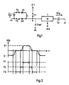
- Cp means the total plasma or panel capacity of a plasma screen, only the circuit elements are shown for the transfer of Cp between O and a positive one Voltage, not the other circuit elements for the corresponding Transfer between O and the negative voltage.
- an additional voltage Uza is added via stage 1, which for serves the addressing of an entire line and thereby one selected line selected.
- For the addressing process given increased tension on each line and additionally a voltage for the column addressing that is on the opposite side of Cp. Through this Row addressing and column addressing each become one pixel or pixel addressed.
- L is the inductance used for energy recovery, in which the stored in Cp in the form of the voltage UCp Energy is recovered in the form of electricity.
- FIG. 2 shows the time course of the voltage UCp across the capacitance Cp for a period.
- the undressed show Lines at T1, T2, T3, during which periods the switches are controlled. It can be seen that the switch T2 in each case during the transitions, ie the reloading of Cp between O and E + is conductive.
- T1 and T3 cause longer ones Connection of the connection a to the voltage E + during the Ignition phase or to earth during the period with the voltage value zero.
- Fig. 1 is only for one polarity shown, i.e. only the connection to E + and earth.
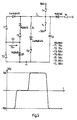
- FIG. 3 shows the expansion of the circuit according to FIG. 2 for both polarities and three voltage values according to FIG. 2.
- E3 -V1 / 2
- E4 + V2 / 2.
- the circuit according to FIG. 3 essentially works on the principle of the circuit according to FIG. 1, the following list of concordances being used for a better understanding: Fig. 4 Fig. 1 T4-, D4- T2, D1 T4, D4 T2, D1 T6, D6 T2, D1 T6-, D6- T2, D1 T5-, D5- T3, D3 T5, D5 T3, D3 T1 T1 T2
- Cp is the total capacity again.
- the actual flow of energy takes place via T1, T2.
- the frequency at which the transhipment takes place is about 30 to 100 kHz.
- Fig. 5 shows an alternative solution to Fig. 3.
- the current for the The ignition phase i.e. the excitation to glow, essentially flows via the transistors TH and TL shown as switches.
- a particularly large plasma screen is necessary because of the higher currents also split into several current paths sensible.
- the transfer of Cp takes place due to the structure of the Switches T1, T2; T3, T1.
- the average voltage of Cp is only zero if the voltages V2 and V1 are symmetrical, i.e. in magnitude are the same.
- Fig. 7 shows a variant for a plasma screen with a large Dimension.
- the majority of the switches TH and TL for the screen transmitting energy is in two parts divided, each of which has a corresponding maintenance circuit THB-TLB is assigned.
- This circuit shows the Possibility to use a common resonance circuit.
- the energy present at the start of the resonance is: 1 2nd C. E 2nd 2nd .
- the delay ⁇ is used for a suitable compensation of the Losses set so that Vp is accurate at the end of the quarter voltage E reached.
Landscapes
- Engineering & Computer Science (AREA)
- Physics & Mathematics (AREA)
- Power Engineering (AREA)
- Plasma & Fusion (AREA)
- Computer Hardware Design (AREA)
- General Physics & Mathematics (AREA)
- Theoretical Computer Science (AREA)
- Control Of Indicators Other Than Cathode Ray Tubes (AREA)
Claims (5)
- Générateur de tension alternative pour la commande d'adressage des lignes d'un écran d'affichage à plasma, dans lequel une connexion (a) d'une capacité d'écran (Cp) peut être connectée cycliquement et consécutivement à différentes tensions de service via un commutateur et dans lequel une inductance (L) servant à la récupération d'énergie est présente sur le trajet du courant de renversement pour la capacité (Cp), caractérisé en ce quela capacité (Cp) peut être connectée à différentes tensions de service (V1, V2, E3+, E4+) via des commutateurs (T1-T6, T4- - T6-) à la suite, de sorte que la tension (UCp) au niveau de la capacité (Cp) présente de façon cyclique trois valeurs de tension différentes et consécutives (V1, V2, 0) séparées par des transitions,et la connexion (a) de la capacité d'écran (Cp) reliée à la première extrémité de l'inductance (L)est reliée à la terre via deux commutateurs parallèles (T5, T5-) à sens de conduction opposé, à une tension de service positive (V2) via un commutateur (T1) et à une deuxième tension de service (V1) via un second commutateur (T2).
- Générateur selon la revendication 1, caractérisé en ce que la seconde extrémité de l'inductance (L) est reliée à la moitié de la première tension de service (E4+) via deux commutateurs parallèles (T4, T4-) à sens de conduction opposé, ainsi qu'à la moitié de la seconde tension de service (E3+) via deux commutateurs parallèles supplémentaires (T6, T6-) à sens de conduction opposé.
- Générateur selon la revendication 1 ou 2, caractérisé en ce que la tension (UCp) au niveau de la capacité (Cp) présente une période de valeur de tension nulle entre une période à tension positive (V2) et une période à tension négative (V1).
- Générateur selon la revendication 3, caractérisé en ce que la tension positive (V2) et la tension négative (V1) sont de grandeurs différentes.
- Générateur selon la revendication 2, 3 ou 4 caractérisé en ce qu'au moins un commutateur (T5, T5-), connecté en parallèle à la capacité d'écran (Cp, Cpanel), ne peut être déconnecté qu'après connexion d'un courant (12) de chargement d'inductance (L) via les commutateurs (T4, T4-, T6, T6-) à la seconde extrémité de l'inductance (L) de sorte que les pertes seront compensées pendant la résonance.
Applications Claiming Priority (3)
| Application Number | Priority Date | Filing Date | Title |
|---|---|---|---|
| DE4321945 | 1993-07-02 | ||
| DE4321945A DE4321945A1 (de) | 1993-07-02 | 1993-07-02 | Wechselspannungsgenerator zur Steuerung eines Plasma-Wiedergabeschirms |
| PCT/EP1994/002057 WO1995001627A1 (fr) | 1993-07-02 | 1994-06-24 | Generateur de tension alternative pour reguler un ecran d'affichage a plasma |
Publications (2)
| Publication Number | Publication Date |
|---|---|
| EP0706703A1 EP0706703A1 (fr) | 1996-04-17 |
| EP0706703B1 true EP0706703B1 (fr) | 1998-09-02 |
Family
ID=6491729
Family Applications (1)
| Application Number | Title | Priority Date | Filing Date |
|---|---|---|---|
| EP94922870A Expired - Lifetime EP0706703B1 (fr) | 1993-07-02 | 1994-06-24 | Generateur de tension alternative pour reguler un ecran d'affichage a plasma |
Country Status (8)
| Country | Link |
|---|---|
| US (1) | US5808420A (fr) |
| EP (1) | EP0706703B1 (fr) |
| JP (1) | JP3423316B2 (fr) |
| KR (1) | KR100333777B1 (fr) |
| CN (1) | CN1101039C (fr) |
| DE (2) | DE4321945A1 (fr) |
| ES (1) | ES2123806T3 (fr) |
| WO (1) | WO1995001627A1 (fr) |
Families Citing this family (39)
| Publication number | Priority date | Publication date | Assignee | Title |
|---|---|---|---|---|
| KR19980023076A (ko) * | 1996-09-25 | 1998-07-06 | 배순훈 | 피디피(pdp)의 전력회수장치 |
| JP2976923B2 (ja) * | 1997-04-25 | 1999-11-10 | 日本電気株式会社 | 容量性負荷の駆動装置 |
| DE19737662A1 (de) * | 1997-08-29 | 1999-03-04 | Thomson Brandt Gmbh | Wechselspannungsgenerator zur Steuerung eines Plasma-Wiedergabeschirms |
| US6407732B1 (en) * | 1998-12-21 | 2002-06-18 | Rose Research, L.L.C. | Low power drivers for liquid crystal display technologies |
| US6917351B1 (en) | 2001-02-06 | 2005-07-12 | Imaging Systems Technology | Energy recovery in plasma display panel |
| KR100428624B1 (ko) * | 2001-08-06 | 2004-04-27 | 삼성에스디아이 주식회사 | 교류 플라즈마 디스플레이 패널의 유지 방전 회로 |
| US6963174B2 (en) * | 2001-08-06 | 2005-11-08 | Samsung Sdi Co., Ltd. | Apparatus and method for driving a plasma display panel |
| KR100463185B1 (ko) * | 2001-10-15 | 2004-12-23 | 삼성에스디아이 주식회사 | 플라즈마 디스플레이 패널, 그의 구동 장치 및 그의 구동방법 |
| KR100477985B1 (ko) * | 2001-10-29 | 2005-03-23 | 삼성에스디아이 주식회사 | 플라즈마 디스플레이 패널, 그의 구동 장치 및 그의 구동방법 |
| KR100425314B1 (ko) * | 2001-12-11 | 2004-03-30 | 삼성전자주식회사 | 전압 스트레스를 개선한 고효율 플라즈마 디스플레이 패널구동 장치 및 방법 |
| TW540026B (en) * | 2001-12-28 | 2003-07-01 | Au Optronics Corp | Method for driving a plasma display panel |
| DE10200827A1 (de) * | 2002-01-11 | 2003-07-24 | Philips Intellectual Property | Verfahren zum Steuern einer Schaltungsanordnung für die Wechselspannungsversorgung eines Plasma-Display-Panels |
| DE10200828A1 (de) * | 2002-01-11 | 2003-07-24 | Philips Intellectual Property | Schaltungsanordnung für die Wechselspannungsversorgung eines Plasma-Display-Panels |
| EP1341144B1 (fr) * | 2002-03-01 | 2006-06-21 | Magnetek S.p.A. | Un circuit de puissance pour écran à plasma |
| US20050082957A1 (en) * | 2002-03-06 | 2005-04-21 | Hoppenbrouwers Jurgen J.L. | Display panel with energy recovery system |
| KR100467450B1 (ko) * | 2002-03-18 | 2005-01-24 | 삼성에스디아이 주식회사 | 플라즈마 디스플레이 패널과 그 구동 장치 및 구동 방법 |
| KR100489274B1 (ko) * | 2002-10-10 | 2005-05-17 | 엘지전자 주식회사 | 플라즈마 디스플레이 패널의 구동장치 |
| EP1548694A4 (fr) * | 2002-10-02 | 2008-03-05 | Fujitsu Hitachi Plasma Display | Circuit de commande et procede de commande |
| JP2004133406A (ja) * | 2002-10-11 | 2004-04-30 | Samsung Sdi Co Ltd | プラズマディスプレイパネルの駆動装置及び駆動方法 |
| KR100502906B1 (ko) * | 2002-10-11 | 2005-07-21 | 삼성에스디아이 주식회사 | 플라즈마 디스플레이 패널의 구동 방법 |
| KR100458574B1 (ko) * | 2002-11-13 | 2004-12-03 | 삼성에스디아이 주식회사 | 플라즈마 디스플레이 패널의 구동 장치 및 방법 |
| KR20040034274A (ko) * | 2002-10-21 | 2004-04-28 | 주식회사 유피디 | 플라즈마 디스플레이 패널의 구동장치 |
| KR100484175B1 (ko) * | 2002-11-08 | 2005-04-18 | 삼성전자주식회사 | 고효율 플라즈마 디스플레이 패널 구동 장치 및 방법 |
| KR100458585B1 (ko) * | 2003-01-22 | 2004-12-03 | 삼성에스디아이 주식회사 | 플라즈마 디스플레이 패널의 구동 장치 및 그 구동 방법 |
| EP1469445A3 (fr) * | 2003-04-16 | 2009-03-04 | Lg Electronics Inc. | Dispositif pour la récupération d'énergie et méthode de commande d'un panneau d'affichage à plasma |
| FR2858727A1 (fr) * | 2003-08-05 | 2005-02-11 | Thomson Plasma | Dispositif de generation d'une rampe de tension dans un circuit de commande pour ecran plasma |
| KR100577763B1 (ko) | 2004-09-08 | 2006-05-10 | 엘지전자 주식회사 | 플라즈마 디스플레이 패널의 구동장치 |
| KR100612507B1 (ko) | 2004-09-07 | 2006-08-14 | 엘지전자 주식회사 | 플라즈마 디스플레이 패널 구동장치 |
| KR100578854B1 (ko) * | 2004-08-18 | 2006-05-11 | 삼성에스디아이 주식회사 | 플라즈마 표시 장치와 그 구동 방법 |
| KR100612508B1 (ko) * | 2004-09-07 | 2006-08-14 | 엘지전자 주식회사 | 플라즈마 표시 패널의 구동 장치 |
| CN100411082C (zh) * | 2004-09-10 | 2008-08-13 | 南京Lg同创彩色显示系统有限责任公司 | 等离子显示器 |
| CN100585676C (zh) * | 2005-01-31 | 2010-01-27 | 株式会社日立等离子体专利许可 | 充放电装置、等离子显示面板和充放电的方法 |
| KR100648685B1 (ko) * | 2005-10-11 | 2006-11-23 | 삼성에스디아이 주식회사 | 플라즈마 표시 장치 및 그 구동 장치와 구동 방법 |
| TWI299153B (en) * | 2005-10-24 | 2008-07-21 | Chunghwa Picture Tubes Ltd | Circuit and method for resetting plasma display panel |
| WO2007094227A1 (fr) * | 2006-02-13 | 2007-08-23 | Matsushita Electric Industrial Co., Ltd. | circuit d'entraînement de panneau d'affichage plasma et dispositif d'affichage plasma |
| CN101030350B (zh) * | 2007-04-04 | 2011-04-20 | 咸阳华清设备科技有限公司 | 完全谐振式pdp能量恢复电路 |
| JP2010249981A (ja) * | 2009-04-14 | 2010-11-04 | Toyo Univ | 容量性負荷駆動回路および表示装置 |
| GB201507474D0 (en) | 2015-04-30 | 2015-06-17 | Shimadzu Corp | A circuit for generating a voltage waveform at an output node |
| CN108538240B (zh) * | 2018-05-29 | 2020-03-10 | 京东方科技集团股份有限公司 | 一种像素驱动电路及其驱动方法、显示装置 |
Family Cites Families (10)
| Publication number | Priority date | Publication date | Assignee | Title |
|---|---|---|---|---|
| JPS5325454B2 (fr) * | 1972-10-18 | 1978-07-27 | ||
| US3938107A (en) * | 1974-07-01 | 1976-02-10 | Ibm Corporation | Gas panel with improved circuit for write operation |
| US4070663A (en) * | 1975-07-07 | 1978-01-24 | Sharp Kabushiki Kaisha | Control system for driving a capacitive display unit such as an EL display panel |
| IT1086808B (it) * | 1976-01-16 | 1985-05-31 | Owens Illinois Inc | Perfezionamento nei dispositivi di presentazione a scarica in gas |
| US4099097A (en) * | 1976-07-02 | 1978-07-04 | Owens-Illinois, Inc. | Driving and addressing circuitry for gas discharge display/memory panels |
| CA1087768A (fr) * | 1976-12-30 | 1980-10-14 | Eugene S. Schlig | Ecriture et effacement dans des afficahges au plasma (ac) |
| US4091309A (en) * | 1977-05-09 | 1978-05-23 | Control Data Corporation | Plasma display drive circuit |
| US4958105A (en) * | 1988-12-09 | 1990-09-18 | United Technologies Corporation | Row driver for EL panels and the like with inductance coupling |
| US5126727A (en) * | 1989-09-25 | 1992-06-30 | Westinghouse Electric Corp. | Power saving drive circuit for tfel devices |
| SU1702419A2 (ru) * | 1990-04-28 | 1991-12-30 | Рязанский Радиотехнический Институт | Устройство дл индикации |
-
1993
- 1993-07-02 DE DE4321945A patent/DE4321945A1/de not_active Withdrawn
-
1994
- 1994-06-24 KR KR1019950706011A patent/KR100333777B1/ko not_active Expired - Fee Related
- 1994-06-24 ES ES94922870T patent/ES2123806T3/es not_active Expired - Lifetime
- 1994-06-24 EP EP94922870A patent/EP0706703B1/fr not_active Expired - Lifetime
- 1994-06-24 CN CN94192549A patent/CN1101039C/zh not_active Expired - Fee Related
- 1994-06-24 JP JP50324895A patent/JP3423316B2/ja not_active Expired - Fee Related
- 1994-06-24 DE DE59406845T patent/DE59406845D1/de not_active Expired - Lifetime
- 1994-06-24 WO PCT/EP1994/002057 patent/WO1995001627A1/fr not_active Ceased
- 1994-06-24 US US08/553,265 patent/US5808420A/en not_active Expired - Lifetime
Also Published As
| Publication number | Publication date |
|---|---|
| JP3423316B2 (ja) | 2003-07-07 |
| EP0706703A1 (fr) | 1996-04-17 |
| KR960703489A (ko) | 1996-08-17 |
| CN1125993A (zh) | 1996-07-03 |
| US5808420A (en) | 1998-09-15 |
| KR100333777B1 (ko) | 2003-01-09 |
| WO1995001627A1 (fr) | 1995-01-12 |
| DE4321945A1 (de) | 1995-01-12 |
| JPH08512140A (ja) | 1996-12-17 |
| CN1101039C (zh) | 2003-02-05 |
| ES2123806T3 (es) | 1999-01-16 |
| DE59406845D1 (de) | 1998-10-08 |
Similar Documents
| Publication | Publication Date | Title |
|---|---|---|
| DE4321945A1 (de) | Wechselspannungsgenerator zur Steuerung eines Plasma-Wiedergabeschirms | |
| DE69519907T2 (de) | Ansteuerschaltung für eine Punktmatrix-AC-Plasmaanzeigetafel mit Memoryeffekt | |
| DE3634686C2 (fr) | ||
| DE68907533T2 (de) | Verfahren zur sehr schnellen Ansteuerung einer wechselspannungsbetriebenen Plasmaanzeigetafel mit koplanarer Unterstützung durch halbselektive Adressierung und selektive Adressierung. | |
| DE69414815T2 (de) | Signalgenerator und Verfahren zur Steuerung eines räumlichen Lichtmodulators | |
| DE60121650T2 (de) | Verfahren und Einrichtung zur Graustufensteuerung von Anzeigetafeln | |
| DE69726246T2 (de) | Wechselrichteranordnung | |
| DE3643149A1 (de) | Treiberschaltung fuer eine duennfilm-elektrolumineszenz(el)-anzeige | |
| DE2349399A1 (de) | Gasentladungssystem | |
| DE69306512T2 (de) | Speisespannungsschaltung für Gatesteuerstufe | |
| DE2423402A1 (de) | Gasentladungsanzeigetafel | |
| DE69732867T2 (de) | Verbesserungen an Schieberegistern unter alleiniger Verwendung von "MIS" Transistoren | |
| DE2327212A1 (de) | Gasentladungsanzeige- und speicherfeld | |
| DE2253969A1 (de) | Verfahren zur steuerung einer gasentladungs-anzeigetafel und anzeigesystem zur durchfuehrung des verfahrens | |
| DE2320073C2 (de) | Steueranordnung für wechselspannungsbetriebene Gasentladungs-Bildschirme | |
| DE602005002754T2 (de) | Flüssigkristall-matrixanzeige | |
| DE69522014T2 (de) | Steuervorrichtung für gemeinsame elektrode in einer flüssigkristallanzeige | |
| DE19737662A1 (de) | Wechselspannungsgenerator zur Steuerung eines Plasma-Wiedergabeschirms | |
| DE69715202T2 (de) | Verfahren zum aktivieren von bildschirmzellen und anzeigegerät zur durchführung dieses verfahrens | |
| DE4117563C2 (de) | Impulsgeneratorschaltung für Zeilenauswahlimpulse und Verfahren zur Erzeugung dieser Impulse | |
| DE2432931B2 (de) | Verfahren zum Steuern eines Gasentladungspaneels | |
| DE2923609C2 (fr) | ||
| DE944141C (de) | Anordnung zum Empfang von Doppelstromtelegrafie mit einem kontaktlosen Relais | |
| DE3852943T2 (de) | Mikrowellen-Röhrenmodulator. | |
| DE69701413T2 (de) | Steuerverfahren für eine Bildanzeigetafel mit Halbtönen und Anzeigeeinrichtung zur Durchführung dieses Verfahrens |
Legal Events
| Date | Code | Title | Description |
|---|---|---|---|
| PUAI | Public reference made under article 153(3) epc to a published international application that has entered the european phase |
Free format text: ORIGINAL CODE: 0009012 |
|
| 17P | Request for examination filed |
Effective date: 19951219 |
|
| AK | Designated contracting states |
Kind code of ref document: A1 Designated state(s): DE ES FR GB IT |
|
| GRAG | Despatch of communication of intention to grant |
Free format text: ORIGINAL CODE: EPIDOS AGRA |
|
| 17Q | First examination report despatched |
Effective date: 19970903 |
|
| GRAG | Despatch of communication of intention to grant |
Free format text: ORIGINAL CODE: EPIDOS AGRA |
|
| GRAH | Despatch of communication of intention to grant a patent |
Free format text: ORIGINAL CODE: EPIDOS IGRA |
|
| GRAG | Despatch of communication of intention to grant |
Free format text: ORIGINAL CODE: EPIDOS AGRA |
|
| GRAH | Despatch of communication of intention to grant a patent |
Free format text: ORIGINAL CODE: EPIDOS IGRA |
|
| GRAA | (expected) grant |
Free format text: ORIGINAL CODE: 0009210 |
|
| AK | Designated contracting states |
Kind code of ref document: B1 Designated state(s): DE ES FR GB IT |
|
| GBT | Gb: translation of ep patent filed (gb section 77(6)(a)/1977) |
Effective date: 19980915 |
|
| REF | Corresponds to: |
Ref document number: 59406845 Country of ref document: DE Date of ref document: 19981008 |
|
| ET | Fr: translation filed | ||
| REG | Reference to a national code |
Ref country code: ES Ref legal event code: FG2A Ref document number: 2123806 Country of ref document: ES Kind code of ref document: T3 |
|
| PLBE | No opposition filed within time limit |
Free format text: ORIGINAL CODE: 0009261 |
|
| STAA | Information on the status of an ep patent application or granted ep patent |
Free format text: STATUS: NO OPPOSITION FILED WITHIN TIME LIMIT |
|
| 26N | No opposition filed | ||
| REG | Reference to a national code |
Ref country code: GB Ref legal event code: 746 Effective date: 20010806 |
|
| REG | Reference to a national code |
Ref country code: GB Ref legal event code: IF02 |
|
| PGFP | Annual fee paid to national office [announced via postgrant information from national office to epo] |
Ref country code: GB Payment date: 20110623 Year of fee payment: 18 |
|
| PGFP | Annual fee paid to national office [announced via postgrant information from national office to epo] |
Ref country code: IT Payment date: 20110621 Year of fee payment: 18 |
|
| PGFP | Annual fee paid to national office [announced via postgrant information from national office to epo] |
Ref country code: FR Payment date: 20110708 Year of fee payment: 18 |
|
| PGFP | Annual fee paid to national office [announced via postgrant information from national office to epo] |
Ref country code: DE Payment date: 20110616 Year of fee payment: 18 Ref country code: ES Payment date: 20110715 Year of fee payment: 18 |
|
| GBPC | Gb: european patent ceased through non-payment of renewal fee |
Effective date: 20120624 |
|
| PG25 | Lapsed in a contracting state [announced via postgrant information from national office to epo] |
Ref country code: IT Free format text: LAPSE BECAUSE OF NON-PAYMENT OF DUE FEES Effective date: 20120624 |
|
| REG | Reference to a national code |
Ref country code: FR Ref legal event code: ST Effective date: 20130228 |
|
| REG | Reference to a national code |
Ref country code: DE Ref legal event code: R119 Ref document number: 59406845 Country of ref document: DE Effective date: 20130101 |
|
| PG25 | Lapsed in a contracting state [announced via postgrant information from national office to epo] |
Ref country code: GB Free format text: LAPSE BECAUSE OF NON-PAYMENT OF DUE FEES Effective date: 20120624 Ref country code: DE Free format text: LAPSE BECAUSE OF NON-PAYMENT OF DUE FEES Effective date: 20130101 Ref country code: FR Free format text: LAPSE BECAUSE OF NON-PAYMENT OF DUE FEES Effective date: 20120702 |
|
| REG | Reference to a national code |
Ref country code: ES Ref legal event code: FD2A Effective date: 20131021 |
|
| PG25 | Lapsed in a contracting state [announced via postgrant information from national office to epo] |
Ref country code: ES Free format text: LAPSE BECAUSE OF NON-PAYMENT OF DUE FEES Effective date: 20120625 |