EP0707416A2 - Bildsensor mit aktiven Bildelementen und Abbildungssystem mit differentieller Betriebsweise - Google Patents
Bildsensor mit aktiven Bildelementen und Abbildungssystem mit differentieller Betriebsweise Download PDFInfo
- Publication number
- EP0707416A2 EP0707416A2 EP95307016A EP95307016A EP0707416A2 EP 0707416 A2 EP0707416 A2 EP 0707416A2 EP 95307016 A EP95307016 A EP 95307016A EP 95307016 A EP95307016 A EP 95307016A EP 0707416 A2 EP0707416 A2 EP 0707416A2
- Authority
- EP
- European Patent Office
- Prior art keywords
- sensor
- voltage
- sensors
- diffusion
- output signal
- Prior art date
- Legal status (The legal status is an assumption and is not a legal conclusion. Google has not performed a legal analysis and makes no representation as to the accuracy of the status listed.)
- Withdrawn
Links
Images


Classifications
-
- H—ELECTRICITY
- H04—ELECTRIC COMMUNICATION TECHNIQUE
- H04N—PICTORIAL COMMUNICATION, e.g. TELEVISION
- H04N25/00—Circuitry of solid-state image sensors [SSIS]; Control thereof
- H04N25/70—SSIS architectures; Circuits associated therewith
- H04N25/76—Addressed sensors, e.g. MOS or CMOS sensors
-
- H—ELECTRICITY
- H04—ELECTRIC COMMUNICATION TECHNIQUE
- H04N—PICTORIAL COMMUNICATION, e.g. TELEVISION
- H04N25/00—Circuitry of solid-state image sensors [SSIS]; Control thereof
- H04N25/70—SSIS architectures; Circuits associated therewith
- H04N25/703—SSIS architectures incorporating pixels for producing signals other than image signals
- H04N25/707—Pixels for event detection
Definitions
- This invention relates generally to improvements in electronic image sensors, and more specifically to active pixel image sensors and imaging systems capable of generating differential output signals.
- CCD charge-coupled device
- a typical CCD imager includes a matrix of photosites that are capable of collecting free electrons that form an electrical charge packet that is directly proportional to the photon radiation incident at that photosite. Accordingly, when an image is focused on the surface of the array, the charge packet at each photosite of the array corresponds to a respective picture element or pixel of the complete image.
- the generated photosite charge packets are transferred in a parallel manner into a CCD shift register, where they are transferred serially as an output signal of the CCD imager.
- the CCD imager output signal is a series of electronic signals whose amplitudes represent the light intensity of the image at each pixel for a single image frame. The process is continuously repeated to generate output signals which correspond to several image frames per second. As a consequence, each frame in the generated output signal contains information concerning the detected light intensity at each photosite.
- a drawback of typical CCD imagers is that they require near-perfect charge transfer over distances on the order of centimeters through semiconductor materials. As a consequence, such CCD imagers require a substantial amount of power and are difficult to use under low light conditions, difficult to manufacture in large array sizes, and difficult to integrate with on-chip electronics.
- Active pixel sensors have become increasingly popular as an alternative to CCD imagers in video equipment. Active pixel sensors employ one or more on-chip transistors at each pixel photosite in the array. The transistors buffer a photo-signal corresponding to the charge packet generated by the photosite and drive an output signal line avoiding the disadvantages of the CCD imager. However, typical active pixel sensor arrays still generate an output signal with each frame containing information concerning the detected light intensity at each photosite.
- an imaging system having a differential output signal employs an array of active pixel sensors arranged into sensor rows and columns. Each sensor collects electrical charge at a photogate corresponding to detected light intensity by the sensor over a frame interval. The generated electrical charge may then be transferred to a buffered diffusion node within the sensor. The voltage at the diffusion node is buffered from other voltage signals generated external to the sensor.
- each active pixel sensor maintains a diffusion node voltage corresponding to a previously detected frame while collecting electrical charge in the photogate corresponding to a present frame.
- a row decoder may be connected to the sensor arrays to simultaneously activate the sensors in a respective row to detect light as well as generate an output voltage signal corresponding to the diffusion node voltage.
- the sensor outputs for a respective column of sensors are connected to a corresponding one of a plurality of differential output circuits.
- the output circuits are also connected to a common output line.
- the differential output circuits are able to temporarily store first and second voltage signals received from the connected sensors which correspond to the diffusion node voltages for the previous and present frames.
- the output circuits further generate a difference signal corresponding to the temporarily stored voltages to the common output line.
- a timing controller may be connected to the row decoder and each differential output circuit to control the system timing.
- the timing controller may cause each sensor row to be sequentially activated to light intensity over a predetermined integration period per frame. At substantially near the end of the integration period for a present frame, the row sensors are activated to generate an output voltage signal.
- each sensor provides to the differential output circuits a first voltage signal corresponding to the existing diffusion node voltage for the previous frame's detected light intensity.
- the sensors are then reset and generate a new diffusion node voltage corresponding to the present frame's detected light intensity. Second voltage signals corresponding to these new node voltages are then provided to the differential output circuits.
- the timing controller may control the differential output circuits to temporarily store the received first and second voltage signals to generate corresponding difference output signals.
- the timing controller may cause the differential output circuits to sequentially provide the difference output signals to the common output line to form the differential output signal.
- the present invention utilities the sensors buffered diffusion node to maintain the previous frame's detected light intensity during the detection of the present frame's light intensity.
- This technique provides the ability to generate a differential output signal without the need of a large memory device or analog-to-digital converters to maintain values for each of the sensors.
- the present invention has reduced power consumption and complexity.
- the present invention may be implemented in a system possessing compact dimensions which will enable it to perform functions previously not thought possible for prior art differential imaging systems, such as in hidden security cameras.
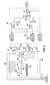
- FIG. 1 shows an active pixel sensor imaging system 1 according to the present invention having an array of active pixel sensors 5, a row decoder 10, a plurality of differential output circuits 18 and a timing controller 20.
- the active pixel sensor array 5 includes ten rows 25 and ten columns 30 of closely spaced active pixel sensors 35.
- the active pixel sensor array 5 is illustrated as a ten-by-ten sensor array for illustrative purposes only and is not meant to be a limitation on the present invention.
- An active pixel sensor array in accordance with the present invention may consist of any number of row and columns of active pixel sensors, and for many applications will typically consist of an array of a large number of pixels.
- Each active pixel sensor 35 is capable of converting a detected quantity of light to a corresponding electrical signal at an output 50.
- a plurality of control lines 55 extend from the row decoder 10 and connect to each of the pixel sensors 35 in a respective sensor row 25.
- the control lines 55 connected to each sensor 35 consist of a photogate control line 180, a reset control line 184 and a select control line 186, as shown in FIG. 2.
- Each active pixel sensor output 50 in a corresponding sensor column 30 is connected by a column output line 65 to a particular differential output circuit 18.
- Each one of the plurality of differential output circuits 18 is further connected to a common imaging system output line 15.
- a differential output signal DIFF is generated by the differential output circuits 18 on the output line 15.
- the differential output signal DIFF may be provided by the output line 15 to other processing circuits 70 to perform, for example, motion detection or video data compression regarding a viewed image.
- the timing controller 20 provides timing signals to the row decoder 10 which sequentially activates each row 25 of active pixel sensors 35 via the control lines 55 to detect light intensity and to generate corresponding output voltage signals during each frame interval.
- a frame refers to a single complete cycle of activating and sensing the output from each sensor 35 in the array 5 a single time over a predetermined frame time period.
- the timing of the imaging system is controlled to achieve a desired frame rate, such as 30 frames per second.
- each sensor row 25 When detecting a particular frame, each sensor row 25 may be activated to detect light intensity over a substantial portion of the frame interval. In the time remaining after the sensor row 25 has detected the light intensity for the frame, each of the respective sensors simultaneously generates output voltage signals corresponding to the amount of light detected by that pixel sensor 35. If an image is focused on the sensor array 5 by, for example, a convention camera lens, then each pixel sensor 35 generates an output voltage signal corresponding to the light intensity for a portion of the image focused on that pixel sensor 35. The output voltage signals generated by the activated sensor row 25 are simultaneously provided to the corresponding differential output circuit 18 via the column output line 65.
- the differential output circuits 18 generate difference output signals based on the corresponding received sensor output signals.
- the generated difference output signals are provided to the output line 15 in a serial fashion to form the differential output signal DIFF based on timing control signals from the timing controller 20.
- the differential output signal DIFF comprises information corresponding to the difference between adjacent frames of the detected image. If there is no motion or change in a scene viewed by the imaging system 1, then the system 1 generates no output signal. If however, a change appears due to motion or a change in the viewed image between consecutive frame readouts, then the imaging system 1 generates a corresponding differential output signal.
- the timing controller 20 controls the row decoder 10 and plurality of differential output circuits 18 to continuously generate the differential output signal DIFF for consecutive frames at the predetermined frame rate.
- Suitable timing control circuits 20 include microprocessor controllers, finite state machine implementations, such as application specific integrated circuits, combinational logic circuits or any other circuit capable of generating the necessary timing signals to the row decoder 10 and the differential output circuits 18.
- the row decoder 10 may be a counter, a demultiplexer or any circuit or device capable of individually activating each sensor row 25. Although the row decoder 10 is shown separate from timing controller 20, a single device or circuit may be employed to perform the functions of these two components in accordance with the present invention.
- Each active pixel sensor 35 in the array 5 may consist of a photosite and one or more on-chip transistors located within each sensor 35 to provide both gain and buffering functions.
- Active pixel sensor refers to devices commonly known in the art as active pixel sensors, as well as any other device or sensor configuration which collects and stores electrical charge in proportion to detected light intensity, and which buffers such stored electrical charge.
- a general description of exemplary active pixel sensors 35, including those having double-polysilicon structures, is provided in, for example, Fossum, E.R "Active Pixel Sensors: Are CCD's Dinosaurs?", Proceeding of SPIE: Charge-Coupled Devices and Solid State Optical Sensors III, Vol. 1900, pp. 2-14 (1993), (“Fossum reference”), which is hereby incorporated by reference.
- FIG. 2 A schematic representation of an exemplary active pixel sensor 35 and a corresponding differential output circuit 18 in accordance with the present invention is shown in FIG. 2.
- the active pixel sensor 35 is connected to the differential output circuit 18 by the corresponding column output line 65. Since other active pixel sensors 35 are also connected to the column output line 65, the line 65 has been shown broken by ellipses 67 in FIG. 2 for clarity.
- the other active pixel sensors 35 may preferably operate in a substantially identical manner to the active pixel sensor 35 shown in FIG. 2. Only one of the differential output circuits 18 has been shown in FIG. 2 for ease of illustration.
- the other differential output circuits 18 will preferably operate in a substantially identical manner to the circuit 18 illustrated in FIG. 2.
- the active pixel sensor 35 may be represented as a photogate 100 charge-coupled to a transfer gate 105 which is further charge-coupled to a diffusion well 110.
- the gates 100 and 105 have gate electrodes 101 and 107, respectively.
- the photogate electrode 101 is connected to the photogate control line 180.
- the transfer gate electrode 107 may be connected to a suitable fixed voltage to enable the transfer of electrical charge from the photogate 100 to the diffusion well 110 as is described below.
- Electrons 102 beneath the photogate 100, electron transfer arrow 106, and transferred electrons 111 in the diffusion well 110 are an electron well representation known in the art to illustrate the transfer of electrical charge from the photogate 100, through the transfer gate 105, to the diffusion well 110.
- the active pixel sensor 35 further includes a reset transistor 120, a voltage-follower transistor 125, a select transistor 130 and a load, such as a suitably biased load transistor 135.
- a diffusion node 115 connects the diffusion well 110 to the reset transistor 120 and the voltage-follower transistor 125.
- the reset and voltage-follower transistors 120, 125 are further connected to a fixed voltage VDD, which will preferably may be five volts if the active pixel sensor 35 is implemented as a CMOS device.
- the reset transistor 120 is also connected to the reset control line 184 of the control lines 55 that extends from the row decoder 10 shown in FIG. 1.
- An output 126 of the voltage-follower transistor 125 is further connected to the select transistor 130 which is connected to the load transistor 135.
- the load transistor 135 is also connected to a fixed load voltage VLOAD and a fixed voltage VSS.
- the fixed voltage VSS will preferably be zero volts if the active pixel sensor 35 is implemented as a CMOS device.
- the select transistor 130 is further connected to the select control line 186 of the control lines 55 shown in FIG. 1.
- the load voltage VLOAD should be adjusted such that a desired resistance value is achieved across the load transistor 135 between the column output line 65 and the fixed voltage VSS.
- the desired resistance value should enable the transistor 125 to operate in a voltage follower mode when the select transistor 130 operates in saturation to effectively act as a closed switch between the transistors 125 and 135.
- Suitable alternatives for the load transistor 135 include on-chip or surface mount resistors, or any other passive or active devices which can provide the required electrical resistance when disposed between the column output line 65 and the fixed voltage VSS.
- the active pixel sensor output 50 shown in FIG. 1, is schematically represented in FIG. 2 by a like numbered connection node between the select transistor 130 and load transistor 135 for clarity.
- the column output line 65 connects the sensor output 50 to the corresponding differential output circuit 18.
- the sensor output signal is provided to first and second single-pole single-throw switches 140, 145 which may be, for example, transistor switches or solid state relays.
- the switches 140, 145 may individually be operated in open or closed positions. In the closed positions, the switches 140, 145 provide a sensor output signal to corresponding first and second charge storage devices, such as capacitors 150 and 155.
- the capacitors 150 and 155 are connected to the fixed voltage VSS as well as respective inputs 161 and 162 of a subtractive signal combiner, such as a differential amplifier 160.
- the switches 140 and 145 are controlled by control signals S1 and S2 generated by the timing control circuit 20.
- An output 163 of the differential amplifier 160 generates the difference output signal which is provided to a third single-pole single-throw switch 170.
- the switch 170 is further connected to the imaging system output line 15.
- the switch 170 operates in an open or closed position, as controlled by a switch control signal S3 generated by the timing controller 20. When closed, the switch 170 provides the difference output signal to the common output line 15.
- the row decoder 10 generates a suitable photogate control signal on a photogate control line 180 to cause the photogates 100 of each sensor 35 in the corresponding row to collect electrical charge based on the detected light intensities.
- the photogate 100 is permitted to collect electrical charge over an integration period, which may be a substantial portion of the frame interval. For instance, if the frame interval is 33 msec., corresponding to 30 frames per second, the integration period may be 33 msec. less approximately one microsecond if the sensor 35 is implemented as a CMOS device.
- the row decoder 10 may cause the biased transfer gate 105 to transfer the collected electrical charge from the photogate 100 to the diffusion well 110 by generating a suitable pulse in the photogate control signal.
- This method of transferring charge is well known in the art and is described in, for example, the above cited Fossum reference.
- a suitable duration for a photogate control signal pulse to cause the transfer gate 105 to transfer the collected electrical charge may be, for example, on the order of one microsecond.
- the fixed transfer gate biasing voltage may be on the order of 2.5 volts if the sensor 35 is implemented as a CMOS device.
- Another well known technique for transferring charge within an active pixel sensor is to clock or pulse the transfer gate electrode when the transfer is required. Both the biasing and clocking techniques cause the voltage potential beneath the transfer gates 105 to be greater than that beneath the photogate 100. Since electrical charge moves from regions of lower potential to regions of higher potential, then the collected charge in the photogate 100 moves to the transfer gate 105 and then to the diffusion well 110.
- the electrical charge maintained in the diffusion well 110 is buffered by the transistors 125 and 130 from signals generated over the corresponding column output line 65 by the other sensors 35 in the column 30.
- the transfer gate 105 further acts to buffer the electrical charge maintained in the diffusion well 110 from that collected by the photogate 100 at all times except when electrical charge is transferred from the photogate 100 to the diffusion well 110.
- the present invention relies on the buffered diffusion nodes 110 to maintain an electrical charge for a previous frame's detected light intensity during the times when the sensor 35 is not generating a voltage output signal and when the photogate 100 of the sensor 35 is collecting electrical charge for a present frame.
- the present invention may use only two charge storage devices 150, 155 and a subtractive signal combiner 160 per sensor column 30 to generate the differential output signal DIFF.
- typical prior art imaging systems required an analog-to-digital converter and an external memory for each light intensity detector in an array to generate such a differential output signal. Therefore, the present invention achieves a substantial advantage of having reduced system complexity, power consumption and size over such prior art imaging systems.
- Each active pixel sensor 35 of the array operates in two different periods during a frame time interval.
- the two periods include a light detection period corresponding to the integration period, and a read out period.
- each sensor row 25 is sequentially activated to detect light during a light detection period and then selected to generate corresponding output signals during the read out period.
- the light detection period and read out period may overlap as is described in detail below with regard to FIG. 3.
- the light detection period may consist of a substantial portion of that interval, and the read out period may be on the order of 10 ⁇ sec. after the light detection period.
- the row decoder 10 may overlap the light detection periods for adjacent sensor rows 25 to achieve the desired frame rate during the read out period. Such an overlapping technique is well known in the imaging system art.
- FIG. 3 shows a timing diagram illustrating one suitable operation of the sensor 35 and output circuit 18 of FIG. 2 in accordance with the present invention.
- FIG. 3 details of waveforms 200 for an overlapping light detection period 202 and read out period 204 of the sensor 35 are shown for a present frame interval. Since the light integration period 202 is much longer than the read out period 204, the waveforms 200 have been shown by ellipses 203 during the light detection period for clarity. "Don't care" regions of the waveforms 200 are illustrated by cross-hatched bars such as region 205 of the waveform 290.
- the row decoder 10, shown in FIG. 1 provides the photogate control signal, illustrated by waveform 270, in a high voltage state to the photogate electrode 101.
- the photogate control signal in the high voltage state causes the sensor photogate 100 to collect electrical charge based on the light intensity focused on that sensor 35 for the present frame.
- the photogate control signal 270 in the high voltage state further prevents the transfer gate 105 from transferring collected electrical charge to the diffusion well 110.
- the electrical charge maintained in the diffusion well 110 is buffered from the photogate 100 during the present frame's light detection period 202 and thus corresponds to the previous frame's detected light intensity.
- the voltage potential at the diffusion node 115 illustrated as waveform 215, corresponds to the electrical charge maintained by the diffusion well 110, it, likewise, corresponds to the previous frame's detected light intensity during the light detection period 202.
- the diffusion node voltage potential 215 corresponding to the previous frame's detected light intensity during this period 202 is represented by a voltage magnitude A in FIG. 3.
- the row decoder 10 initiates the read out period by generating the select control signal, illustrated as waveform 220, in a high voltage state.
- the select control signal 220 remains in a high voltage state for the duration of the read out period 204 and is in a low voltage state at all other times.
- the high voltage state select control signal 220 causes the select transistor 130 in FIG. 2, normally in an "off' state, to operate in saturation or in an "on" state.
- the select transistor 130 When operated in the on state, the select transistor 130 acts effectively as a closed switch which enables the transistor 125 to operate as a voltage-follower. While the transistor 125 operates as a voltage follower it generates a voltage at its output 126 and a voltage signal at the sensor output 50 that corresponds to the voltage potential 215 at the diffusion node 115. Since the diffusion node voltage potential 215 is a voltage of amplitudes A at time T1, the output voltage signal 230 illustrated as waveform 230, may also be considered an amplitude of A volts at time T1. Prior to time T1, the select transistor is in the "off' state and no output voltage signal is generated, as indicated by the "don't care" region 206. Further, since the diffusion node voltage potential 215 at time T1 corresponds to the previous frame's detected light intensity, the output signal 230 generated immediately after the time T1 also corresponds to the previous frame's detected light intensity.
- the closing of switch 140 permits the sensor output voltage signal 230 to charge the capacitor 150.
- the switch control signal S1 240 is generated in a low voltage state causing the switch 140 to open.
- the time duration between times T2 and T3 should be selected to permit the capacitor 150 to sufficiently charge to a voltage potential corresponding to the received sensor output voltage signal 230 having the voltage A.
- a suitable charging time for the capacitor 150 is on the order of one microsecond.
- the charge stored in the capacitor 150 corresponds to the amount of detected light by the sensor 35 for the previous frame.
- the row decoder 10 After the voltage A has been stored in the first capacitor 150, such as at time T4, the row decoder 10 generates the reset signal pulse on the reset control line 55 in a high voltage state, as shown by waveform 260.
- This reset signal pulse 260 causes the reset transistor 120 to operate in the on state which forces the diffusion node 115 to the voltage VDD.
- the corresponding sensor output signal 230 likewise, increases to a voltage corresponding to the voltage VDD.
- the light detection and read out periods 202, 204 overlap between times T1 and T5. Shortly after the reset pulse has concluded, such as at time T5, the light detection period 202 ends and a low voltage pulse 275 is generated for the photogate control signal 270.
- the low voltage pulse 275, between times T5 and T6, causes the collected electrical charge in the photogate 100 to transfer to the diffusion well 110 in a manner described above with regard to FIG. 2.
- This transfer of electrical charge causes the diffusion node voltage 215 and the corresponding output voltage signal 230 to lower in proportion to the amount of collected charge or the detected light intensity for the present frame.
- the greater the light intensity the greater the amount of collected charge and the greater the amount that the corresponding diffusion node voltage 215 is lowered.
- the output voltage signal 230 provided to the output circuit 18 corresponds to the detected light intensity for the present frame.
- the magnitude of the sensor output signal 230 shortly after time T5 is illustrated as a voltage B in FIG. 3.
- the timing control device 20 closes the second switch 150 by generating the switch control signal S2 in a high voltage state as shown by the waveform 280.
- the closing of the switch 145 causes the second capacitor 155 to charge to approximately the sensor output voltage signal 230, or in other words, to a value proportional to the voltage B.
- the timing control unit 20 generates the signal S2 in a low voltage state to cause the switch 145 to open.
- the differential amplifier After time T8, the voltages across the capacitors 150 and 155 correspond to the voltages A and B, respectively. As a consequence, after time T8, the differential amplifier generates a difference output signal 290 that is a voltage corresponding to the difference between the voltages A and B. Prior to time T8, the waveform 290 consists of the "don't care" region 205. Since the voltages across the capacitors 150 and 155 represent the light intensity detected by the sensor 35 for the previous and present frames, the generated sensor difference signal represents the difference of the detected light intensity by the sensor 35 between the frames.
- the timing controller 20 generates switch control signal S3 to close the switch 170 which provides the difference output signal to the imaging system output line 15.
- the switch 170 is only closed at a particular time and for the proper duration, in order to insert the sensor differential output signal into its proper sequence position within the imaging system differential output signal DIFF.
- Each pixel sensor 35 in each array row 25 is preferably operated in the same manner as is described above with regard to FIG. 3 to generate a differential output signal for a frame of a detected image. Since the voltage potential present at the diffusion node 115 of each sensor 35 is buffered from the corresponding photogate 100 and column output line 65, it maintains a voltage potential based on an amount of detected light from frame to frame. As a consequence, the voltage potential at the diffusion node 115 remains a voltage corresponding to the voltage B until that sensor 35 again enters a read out period for the next detected frame, as shown at time T9 in FIG. 3. Accordingly, during read out of the sensor 35 for the next frame at time T9, the sensor output voltage signal 230, corresponding to the previous frame, is the voltage B.
- the photogate 100 does not collect charge while the voltage signal applied to its gate electrode 101 is in a low voltage state, such as between times T5 and T6. Further, the light detection period for the next frame begins at the conclusion of the low voltage pulse 275 on the photogate control signal 270 at time T6. In this manner, the amount of time that each pixel sensor 35 is not detecting light for each frame is minimized. The next frame's light detection period ends at the next generation of a low voltage pulse for the photogate control signal 270 which occurs at the appropriate time some time after time T9. The timing controller 20 continuously repeats this operation with the proper timing to achieve the differential output signal DIFF having the desired frame rate.
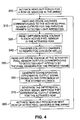
- FIG. 4 is a flow diagram summarizing an exemplary image detection method for generating the differential output signal DIFF in accordance with the present invention. Steps 300-380 of FIG. 4 are recited in terms of the events during the read out periods of each active pixel sensor 35. The generation of the corresponding photogate control signal 270 and corresponding light detection period are timed so as to enable the performance of steps 300-380 as indicated in FIG. 4.
- an active pixel sensor row 25 in the array 5 is first activated for read out by generating the appropriate select control signal on the corresponding select control line 186 in step 300.
- each of the sensors 35 When activated for read out, each of the sensors 35 generates a voltage signal at its respective output 50 representing the voltage potential present at its diffusion node 115. Since the activated sensors 35 have not been reset, the diffusion node voltages and the corresponding output voltage signals at the sensor outputs 50 correspond to the light intensities detected by sensors 35 for the previous frame.
- step 310 corresponds to the closing of the first switch 140 and the resulting charging of the first capacitor 150 by the sensor output voltage signal, as described above with respect to FIGS. 2 and 3.
- step 320 the diffusion nodes 115 of the activated sensors 35 are then reset to a reset voltage as indicated in step 320. Resetting of a diffusion node 115 may be accomplished with a high voltage pulse provided to the corresponding reset transistor 120 as described above with respect to FIGS. 2 and 3.
- step 340 the electrical charges collected by the photogates 100 in the activated sensor row 25 are transferred to the respective diffusion wells 110.
- transferring the collected electrical charges to the respective diffusion wells 110 causes the voltage of the diffusion nodes 115 to lower from their reset voltage.
- the voltages present at the activated sensors' diffusion nodes 115 and the corresponding output voltage signals provided to the differential output circuits 18 represent the detected light intensity for the present frame.
- the voltage output signals for the present frame are then read and stored by the corresponding differential output circuits 18 in step 350.
- the sensor output voltage signals are read and stored by charging the second charge storage devices 155.
- the differential output circuits 18 maintain voltage potentials for the present and previous frames' detected light intensities.
- step 360 a difference is taken of the stored voltages in each output circuit 18 to yield difference output signals.
- This step may be accomplished using the differential amplifier 160 of FIG. 2.
- the difference output signals correspond to the frame-to-frame difference in the amount of detected light intensity for each of the activated pixel sensors 35.
- the difference output signals are then sequentially provided to the imaging system output line 15, shown in FIG. 1, in a predetermined order in step 370 to form the differential output signal DIFF.
- the output signal DIFF is a serially transmitted compilation of the difference output signals for the sensors 35 of the activated row 25.
- the next sensor row 25 is then activated for read out by the appropriate corresponding select control line 60 in step 380.
- Steps 310-370 are then repeated for the newly activated sensor row 25 to generate the respective difference output signals to form the corresponding portion of the differential output signal DIFF.
- the image detection method of FIG. 4 continuously generates difference output signals for each sensor row 25 to produce the differential output signal DIFF for consecutive detected frames during the time that the imaging system is operational.
- the differential output circuit 18 may use one single-throw double-pole switch instead of the two switches 140, 145, or may consist of any configuration of components capable of providing two serially received voltage signals to a signal combiner in a parallel fashion, and generating a difference signal based on the two voltage signals.
- Other active pixel sensor implementations with different voltages may be readily employed.
- the array of FIG. 1 has been arranged into the activation of rows and the read out of columns, the present invention may connect any number of active pixel sensors at any array position to a corresponding differential output circuit.
Landscapes
- Engineering & Computer Science (AREA)
- Multimedia (AREA)
- Signal Processing (AREA)
- Solid State Image Pick-Up Elements (AREA)
- Transforming Light Signals Into Electric Signals (AREA)
Applications Claiming Priority (2)
| Application Number | Priority Date | Filing Date | Title |
|---|---|---|---|
| US323203 | 1994-10-14 | ||
| US08/323,203 US5631704A (en) | 1994-10-14 | 1994-10-14 | Active pixel sensor and imaging system having differential mode |
Publications (2)
| Publication Number | Publication Date |
|---|---|
| EP0707416A2 true EP0707416A2 (de) | 1996-04-17 |
| EP0707416A3 EP0707416A3 (de) | 1996-09-04 |
Family
ID=23258157
Family Applications (1)
| Application Number | Title | Priority Date | Filing Date |
|---|---|---|---|
| EP95307016A Withdrawn EP0707416A3 (de) | 1994-10-14 | 1995-10-03 | Bildsensor mit aktiven Bildelementen und Abbildungssystem mit differentieller Betriebsweise |
Country Status (4)
| Country | Link |
|---|---|
| US (1) | US5631704A (de) |
| EP (1) | EP0707416A3 (de) |
| JP (1) | JPH08181920A (de) |
| CA (1) | CA2156946A1 (de) |
Cited By (12)
| Publication number | Priority date | Publication date | Assignee | Title |
|---|---|---|---|---|
| US5898753A (en) * | 1997-06-06 | 1999-04-27 | Schick Technologies, Inc. | Apparatus for measuring bone density using active pixel sensors |
| US5912942A (en) * | 1997-06-06 | 1999-06-15 | Schick Technologies, Inc. | X-ray detection system using active pixel sensors |
| WO2000005874A1 (en) * | 1998-07-22 | 2000-02-03 | Foveon, Inc. | Multiple storage node active pixel sensors |
| WO2000051344A1 (en) * | 1999-02-26 | 2000-08-31 | Intel Corporation | An improved light sensor with increased dynamic range |
| US6410899B1 (en) | 1998-06-17 | 2002-06-25 | Foveon, Inc. | Active pixel sensor with bootstrap amplification and reduced leakage during readout |
| US6525304B1 (en) | 2000-11-28 | 2003-02-25 | Foveon, Inc. | Circuitry for converting analog signals from pixel sensor to a digital and for storing the digital signal |
| US6697114B1 (en) | 1999-08-13 | 2004-02-24 | Foveon, Inc. | Triple slope pixel sensor and arry |
| US6760070B1 (en) | 2000-02-29 | 2004-07-06 | Foveon, Inc. | High-sensitivity storage pixel sensor array having auto-exposure detection |
| US6809768B1 (en) | 2000-02-14 | 2004-10-26 | Foveon, Inc. | Double slope pixel sensor and array |
| EP1463306A3 (de) * | 2003-03-25 | 2008-01-23 | Matsushita Electric Industrial Co., Ltd. | Bildaufnahmevorrichtung, die Detailverlust schattiger Bereiche vermeidet |
| EP2821937A1 (de) * | 2013-07-02 | 2015-01-07 | MBDA France | Verfahren und Vorrichtung zur Detektion von Mündungsfeuern von Leichtwaffen |
| CN114125332A (zh) * | 2020-09-01 | 2022-03-01 | 原相科技股份有限公司 | 像素电路及像素阵列的运行方法 |
Families Citing this family (134)
| Publication number | Priority date | Publication date | Assignee | Title |
|---|---|---|---|---|
| US6456326B2 (en) | 1994-01-28 | 2002-09-24 | California Institute Of Technology | Single chip camera device having double sampling operation |
| USRE42918E1 (en) | 1994-01-28 | 2011-11-15 | California Institute Of Technology | Single substrate camera device with CMOS image sensor |
| US6166768A (en) * | 1994-01-28 | 2000-12-26 | California Institute Of Technology | Active pixel sensor array with simple floating gate pixels |
| US6486503B1 (en) | 1994-01-28 | 2002-11-26 | California Institute Of Technology | Active pixel sensor array with electronic shuttering |
| US5471515A (en) | 1994-01-28 | 1995-11-28 | California Institute Of Technology | Active pixel sensor with intra-pixel charge transfer |
| US5576763A (en) * | 1994-11-22 | 1996-11-19 | Lucent Technologies Inc. | Single-polysilicon CMOS active pixel |
| SE9502063L (sv) * | 1995-06-07 | 1996-10-28 | Integrated Vision Prod | Anordning för inläsning och behandling av bildinformation |
| JP3031606B2 (ja) * | 1995-08-02 | 2000-04-10 | キヤノン株式会社 | 固体撮像装置と画像撮像装置 |
| EP0878007B1 (de) * | 1996-01-22 | 2005-05-11 | California Institute Of Technology | Aktive bildelementsensormatrix mit elektronischer überblendung |
| JP3774499B2 (ja) * | 1996-01-24 | 2006-05-17 | キヤノン株式会社 | 光電変換装置 |
| US5881184A (en) * | 1996-05-22 | 1999-03-09 | Eastman Kodak Company | Active pixel sensor with single pixel reset |
| US5949061A (en) * | 1997-02-27 | 1999-09-07 | Eastman Kodak Company | Active pixel sensor with switched supply row select |
| EP0809394B1 (de) * | 1996-05-22 | 2008-02-13 | Eastman Kodak Company | Aktives Bildelement mit einer über eine geschaltete Versorgungsspannung gesteuerte Zeilenauswahl |
| US5986297A (en) * | 1996-05-22 | 1999-11-16 | Eastman Kodak Company | Color active pixel sensor with electronic shuttering, anti-blooming and low cross-talk |
| US6550949B1 (en) | 1996-06-13 | 2003-04-22 | Gentex Corporation | Systems and components for enhancing rear vision from a vehicle |
| US6452632B1 (en) | 1997-01-31 | 2002-09-17 | Kabushiki Kaisha Toshiba | Solid state image sensor and video system using the same |
| US5939742A (en) * | 1997-02-10 | 1999-08-17 | Lucent Technologies Inc. | Field-effect photo-transistor |
| US6160281A (en) | 1997-02-28 | 2000-12-12 | Eastman Kodak Company | Active pixel sensor with inter-pixel function sharing |
| JP3695933B2 (ja) * | 1997-03-18 | 2005-09-14 | 株式会社東芝 | 固体撮像装置 |
| US5892253A (en) * | 1997-03-26 | 1999-04-06 | Foveonics, Inc. | Active pixel sensor cell with balanced blue response and reduced noise |
| US5920345A (en) * | 1997-06-02 | 1999-07-06 | Sarnoff Corporation | CMOS image sensor with improved fill factor |
| US6320616B1 (en) | 1997-06-02 | 2001-11-20 | Sarnoff Corporation | CMOS image sensor with reduced fixed pattern noise |
| US5923369A (en) * | 1997-07-23 | 1999-07-13 | Foveonics, Inc. | Active pixel sensor cell with differential amplifier and array including same |
| US6798452B1 (en) | 1997-07-28 | 2004-09-28 | Matsushita Electric Industrial Co., Ltd. | Amplifying solid-state imaging device, method for driving the same and physical quantity distribution sensing semiconductor device |
| US5900623A (en) * | 1997-08-11 | 1999-05-04 | Chrontel, Inc. | Active pixel sensor using CMOS technology with reverse biased photodiodes |
| US6624849B1 (en) | 1997-12-08 | 2003-09-23 | Nikon Corporation | Solid-state imaging apparatus for motion detection |
| US6753904B1 (en) * | 1997-08-12 | 2004-06-22 | Nikon Corporation | Solid-state imaging apparatus for motion detection |
| US5898196A (en) * | 1997-10-10 | 1999-04-27 | International Business Machines Corporation | Dual EPI active pixel cell design and method of making the same |
| US6233013B1 (en) | 1997-10-23 | 2001-05-15 | Xerox Corporation | Color readout system for an active pixel image sensor |
| US6369853B1 (en) | 1997-11-13 | 2002-04-09 | Foveon, Inc. | Intra-pixel frame storage element, array, and electronic shutter method suitable for electronic still camera applications |
| US5909041A (en) * | 1997-11-21 | 1999-06-01 | Xerox Corporation | Photogate sensor with improved responsivity |
| JPH11164210A (ja) | 1997-11-28 | 1999-06-18 | Nikon Corp | 動き検出用固体撮像装置 |
| US6008486A (en) * | 1997-12-31 | 1999-12-28 | Gentex Corporation | Wide dynamic range optical sensor |
| CA2320153A1 (en) * | 1997-12-31 | 1999-07-08 | Gentex Corporation | Vehicle vision system |
| US6201572B1 (en) * | 1998-02-02 | 2001-03-13 | Agilent Technologies, Inc. | Analog current mode assisted differential to single-ended read-out channel operable with an active pixel sensor |
| US6365886B1 (en) | 1998-02-18 | 2002-04-02 | Photobit Corporation | Smart column controls for high speed multi-resolution sensors |
| US6388241B1 (en) | 1998-02-19 | 2002-05-14 | Photobit Corporation | Active pixel color linear sensor with line—packed pixel readout |
| US6452633B1 (en) | 1998-02-26 | 2002-09-17 | Foveon, Inc. | Exposure control in electronic cameras by detecting overflow from active pixels |
| NL1011406C2 (nl) | 1998-02-28 | 2000-01-07 | Hyundai Electronics Ind | CMOS beeldsensor met testschakeling voor het verifiëren van de werking daarvan. |
| US6847399B1 (en) * | 1998-03-23 | 2005-01-25 | Micron Technology, Inc. | Increasing readout speed in CMOS APS sensors through block readout |
| US6069376A (en) * | 1998-03-26 | 2000-05-30 | Foveonics, Inc. | Intra-pixel frame storage element, array, and electronic shutter method including speed switch suitable for electronic still camera applications |
| US6160282A (en) * | 1998-04-21 | 2000-12-12 | Foveon, Inc. | CMOS image sensor employing silicide exclusion mask to reduce leakage and improve performance |
| US6741282B1 (en) | 1998-05-05 | 2004-05-25 | Intel Corporation | Method and apparatus for processing a photocurrent in both discrete and continuous time |
| KR19990084630A (ko) | 1998-05-08 | 1999-12-06 | 김영환 | 씨모스 이미지 센서 및 그 구동 방법 |
| US6476864B1 (en) | 1998-05-11 | 2002-11-05 | Agilent Technologies, Inc. | Pixel sensor column amplifier architecture |
| US6512544B1 (en) | 1998-06-17 | 2003-01-28 | Foveon, Inc. | Storage pixel sensor and array with compression |
| US6054704A (en) | 1998-06-30 | 2000-04-25 | Foveon, Inc. | Driven capacitor storage pixel sensor and array |
| US6512858B2 (en) | 1998-07-21 | 2003-01-28 | Foveon, Inc. | Image scanning circuitry with row and column addressing for use in electronic cameras |
| WO2000007360A1 (en) * | 1998-07-31 | 2000-02-10 | Intel Corporation | An improved light sensor and a method of employing the improved light sensor to capture and process image data |
| US6246043B1 (en) | 1998-09-22 | 2001-06-12 | Foveon, Inc. | Method and apparatus for biasing a CMOS active pixel sensor above the nominal voltage maximums for an IC process |
| US6677997B1 (en) | 1998-11-05 | 2004-01-13 | Matsushita Electric Industrial Co., Ltd. | Amplifying solid-state imaging device, and method for driving the same |
| US6147846A (en) * | 1998-12-01 | 2000-11-14 | Agilent Technologies, Inc. | Drive circuit with over-voltage protection for use with pixel cells and other circuits |
| US6218656B1 (en) | 1998-12-30 | 2001-04-17 | Eastman Kodak Company | Photodiode active pixel sensor with shared reset signal row select |
| US6624850B1 (en) | 1998-12-30 | 2003-09-23 | Eastman Kodak Company | Photogate active pixel sensor with high fill factor and correlated double sampling |
| US6657665B1 (en) | 1998-12-31 | 2003-12-02 | Eastman Kodak Company | Active Pixel Sensor with wired floating diffusions and shared amplifier |
| US6803958B1 (en) * | 1999-03-09 | 2004-10-12 | Micron Technology, Inc. | Apparatus and method for eliminating artifacts in active pixel sensor (APS) imagers |
| US6859227B1 (en) * | 1999-04-23 | 2005-02-22 | Micron Technology, Inc. | Active pixel sensor with reduced fixed pattern noise |
| US6777663B2 (en) * | 1999-05-07 | 2004-08-17 | Intel Corporation | Enhanced Photocell with sample and hold amplifier |
| US6597398B1 (en) * | 1999-06-02 | 2003-07-22 | Intel Corporation | Image sensor response enhancement using fluorescent phosphors |
| FR2795587B1 (fr) * | 1999-06-23 | 2001-09-07 | Agence Spatiale Europeenne | Detecteur du type a pixels actifs |
| JP4337177B2 (ja) * | 1999-07-09 | 2009-09-30 | ソニー株式会社 | 固体撮像素子およびその駆動方法 |
| US6285018B1 (en) | 1999-07-20 | 2001-09-04 | Intevac, Inc. | Electron bombarded active pixel sensor |
| US6657178B2 (en) | 1999-07-20 | 2003-12-02 | Intevac, Inc. | Electron bombarded passive pixel sensor imaging |
| US6307586B1 (en) | 1999-07-20 | 2001-10-23 | Intevac, Inc. | Electron bombarded active pixel sensor camera incorporating gain control |
| US6218692B1 (en) | 1999-11-23 | 2001-04-17 | Eastman Kodak Company | Color active pixel sensor with electronic shuttering, anti-blooming and low cross talk |
| US6365926B1 (en) | 2000-09-20 | 2002-04-02 | Eastman Kodak Company | CMOS active pixel with scavenging diode |
| US6950131B1 (en) * | 2000-09-26 | 2005-09-27 | Valley Oak Semiconductor | Simultaneous access and reset system for an active pixel sensor |
| JP4736173B2 (ja) * | 2000-10-27 | 2011-07-27 | 株式会社ニコン | 撮像装置 |
| US6504195B2 (en) | 2000-12-29 | 2003-01-07 | Eastman Kodak Company | Alternate method for photodiode formation in CMOS image sensors |
| WO2002089038A2 (en) | 2001-04-27 | 2002-11-07 | Atrua Technologies, Inc. | Capacitive sensor system with improved capacitance measuring sensitivity |
| US7259573B2 (en) * | 2001-05-22 | 2007-08-21 | Atrua Technologies, Inc. | Surface capacitance sensor system using buried stimulus electrode |
| JP2005516377A (ja) * | 2001-05-22 | 2005-06-02 | アトルア テクノロジーズ インコーポレイテッド | 集積回路センサのための改善された接続組立体 |
| US7088394B2 (en) | 2001-07-09 | 2006-08-08 | Micron Technology, Inc. | Charge mode active pixel sensor read-out circuit |
| US20030115490A1 (en) | 2001-07-12 | 2003-06-19 | Russo Anthony P. | Secure network and networked devices using biometrics |
| JP4164263B2 (ja) * | 2002-01-29 | 2008-10-15 | キヤノン株式会社 | 固体撮像装置、カメラ及び情報処理装置 |
| US7189951B2 (en) * | 2002-04-09 | 2007-03-13 | Canon Kabushiki Kaisha | Solid-state image sensing apparatus and image sensing system |
| US6903670B1 (en) | 2002-10-04 | 2005-06-07 | Smal Camera Technologies | Circuit and method for cancellation of column pattern noise in CMOS imagers |
| GB0224770D0 (en) * | 2002-10-24 | 2002-12-04 | Council Cent Lab Res Councils | Imaging device |
| US7408577B2 (en) * | 2003-04-09 | 2008-08-05 | Micron Technology, Inc. | Biasing scheme for large format CMOS active pixel sensors |
| US20050012968A1 (en) * | 2003-07-14 | 2005-01-20 | Dialog Semiconductor | Pixel with variable resolution during exposure |
| US7692219B1 (en) | 2004-06-25 | 2010-04-06 | University Of Hawaii | Ultrasensitive biosensors |
| US7785785B2 (en) | 2004-11-12 | 2010-08-31 | The Board Of Trustees Of The Leland Stanford Junior University | Charge perturbation detection system for DNA and other molecules |
| US7643056B2 (en) * | 2005-03-14 | 2010-01-05 | Aptina Imaging Corporation | Motion detecting camera system |
| US7488083B2 (en) * | 2005-08-22 | 2009-02-10 | Gentex Corporation | Vehicular rearview components and assemblies |
| JP4486015B2 (ja) * | 2005-09-13 | 2010-06-23 | パナソニック株式会社 | 固体撮像装置 |
| US20070191910A1 (en) * | 2006-02-16 | 2007-08-16 | Qiushi Ren | Visual prosthesis |
| US8197539B2 (en) * | 2006-05-05 | 2012-06-12 | University Of Southern California | Intraocular camera for retinal prostheses |
| US20080031593A1 (en) * | 2006-08-07 | 2008-02-07 | Shih-Fang Chuang | Multi-layer structure unit for recording audio/video frame data and its operation method |
| JP4928199B2 (ja) * | 2006-09-07 | 2012-05-09 | キヤノン株式会社 | 信号検出装置、信号検出装置の信号読み出し方法及び信号検出装置を用いた撮像システム |
| US8262900B2 (en) | 2006-12-14 | 2012-09-11 | Life Technologies Corporation | Methods and apparatus for measuring analytes using large scale FET arrays |
| US8349167B2 (en) | 2006-12-14 | 2013-01-08 | Life Technologies Corporation | Methods and apparatus for detecting molecular interactions using FET arrays |
| GB2457851B (en) | 2006-12-14 | 2011-01-05 | Ion Torrent Systems Inc | Methods and apparatus for measuring analytes using large scale fet arrays |
| US11339430B2 (en) | 2007-07-10 | 2022-05-24 | Life Technologies Corporation | Methods and apparatus for measuring analytes using large scale FET arrays |
| US7944020B1 (en) | 2006-12-22 | 2011-05-17 | Cypress Semiconductor Corporation | Reverse MIM capacitor |
| EP2307577B1 (de) | 2008-06-25 | 2015-06-03 | Life Technologies Corporation | Verfahren zur analytmessung mithilfe grosser fet-arrays |
| US20100137143A1 (en) | 2008-10-22 | 2010-06-03 | Ion Torrent Systems Incorporated | Methods and apparatus for measuring analytes |
| US20100301398A1 (en) | 2009-05-29 | 2010-12-02 | Ion Torrent Systems Incorporated | Methods and apparatus for measuring analytes |
| US8258451B2 (en) * | 2009-01-15 | 2012-09-04 | Raytheon Company | Image capture system including multipurpose photodetector |
| US8776573B2 (en) | 2009-05-29 | 2014-07-15 | Life Technologies Corporation | Methods and apparatus for measuring analytes |
| US20120261274A1 (en) | 2009-05-29 | 2012-10-18 | Life Technologies Corporation | Methods and apparatus for measuring analytes |
| TWI465716B (zh) | 2010-06-30 | 2014-12-21 | 生命技術公司 | 用於檢測及測量化學反應及化合物之電晶體電路 |
| EP2588850B1 (de) | 2010-06-30 | 2016-12-28 | Life Technologies Corporation | Trockentestverfahren für isfet-arrays |
| EP2588851B1 (de) | 2010-06-30 | 2016-12-21 | Life Technologies Corporation | Ion-sensing charge-accumulation circuit and method |
| US11307166B2 (en) | 2010-07-01 | 2022-04-19 | Life Technologies Corporation | Column ADC |
| US8653567B2 (en) | 2010-07-03 | 2014-02-18 | Life Technologies Corporation | Chemically sensitive sensor with lightly doped drains |
| DE102010035811B4 (de) | 2010-08-30 | 2024-01-25 | Arnold & Richter Cine Technik Gmbh & Co. Betriebs Kg | Bildsensor und Verfahren zum Auslesen eines Bildsensors |
| WO2012036679A1 (en) | 2010-09-15 | 2012-03-22 | Life Technologies Corporation | Methods and apparatus for measuring analytes |
| US8685324B2 (en) | 2010-09-24 | 2014-04-01 | Life Technologies Corporation | Matched pair transistor circuits |
| US9052497B2 (en) | 2011-03-10 | 2015-06-09 | King Abdulaziz City For Science And Technology | Computing imaging data using intensity correlation interferometry |
| US9099214B2 (en) | 2011-04-19 | 2015-08-04 | King Abdulaziz City For Science And Technology | Controlling microparticles through a light field having controllable intensity and periodicity of maxima thereof |
| US9970984B2 (en) | 2011-12-01 | 2018-05-15 | Life Technologies Corporation | Method and apparatus for identifying defects in a chemical sensor array |
| DE102011120099B4 (de) | 2011-12-02 | 2024-05-29 | Arnold & Richter Cine Technik Gmbh & Co. Betriebs Kg | Bildsensor und Verfahren zum Auslesen eines Bildsensors |
| US8821798B2 (en) | 2012-01-19 | 2014-09-02 | Life Technologies Corporation | Titanium nitride as sensing layer for microwell structure |
| US8747748B2 (en) | 2012-01-19 | 2014-06-10 | Life Technologies Corporation | Chemical sensor with conductive cup-shaped sensor surface |
| US8786331B2 (en) | 2012-05-29 | 2014-07-22 | Life Technologies Corporation | System for reducing noise in a chemical sensor array |
| US9080968B2 (en) | 2013-01-04 | 2015-07-14 | Life Technologies Corporation | Methods and systems for point of use removal of sacrificial material |
| US9841398B2 (en) | 2013-01-08 | 2017-12-12 | Life Technologies Corporation | Methods for manufacturing well structures for low-noise chemical sensors |
| US8962366B2 (en) | 2013-01-28 | 2015-02-24 | Life Technologies Corporation | Self-aligned well structures for low-noise chemical sensors |
| US8841217B1 (en) | 2013-03-13 | 2014-09-23 | Life Technologies Corporation | Chemical sensor with protruded sensor surface |
| US8963216B2 (en) | 2013-03-13 | 2015-02-24 | Life Technologies Corporation | Chemical sensor with sidewall spacer sensor surface |
| WO2014149779A1 (en) | 2013-03-15 | 2014-09-25 | Life Technologies Corporation | Chemical device with thin conductive element |
| US9116117B2 (en) | 2013-03-15 | 2015-08-25 | Life Technologies Corporation | Chemical sensor with sidewall sensor surface |
| CN105264366B (zh) | 2013-03-15 | 2019-04-16 | 生命科技公司 | 具有一致传感器表面区域的化学传感器 |
| EP2972279B1 (de) | 2013-03-15 | 2021-10-06 | Life Technologies Corporation | Chemischer sensor mit stetigen sensoroberflächen |
| US9835585B2 (en) | 2013-03-15 | 2017-12-05 | Life Technologies Corporation | Chemical sensor with protruded sensor surface |
| JP6195728B2 (ja) * | 2013-04-30 | 2017-09-13 | 富士フイルム株式会社 | 固体撮像素子および撮像装置 |
| US20140336063A1 (en) | 2013-05-09 | 2014-11-13 | Life Technologies Corporation | Windowed Sequencing |
| JP6134979B2 (ja) * | 2013-06-04 | 2017-05-31 | 富士フイルム株式会社 | 固体撮像素子および撮像装置 |
| US10458942B2 (en) | 2013-06-10 | 2019-10-29 | Life Technologies Corporation | Chemical sensor array having multiple sensors per well |
| DE102015003134B4 (de) * | 2014-04-01 | 2017-04-06 | Viimagic Gesellschaft mit beschränkter Haftung | Global-Shutter Pixel und Korrekturverfahren |
| KR102593647B1 (ko) | 2014-12-18 | 2023-10-26 | 라이프 테크놀로지스 코포레이션 | 트랜스미터 구성을 갖춘 높은 데이터율 집적 회로 |
| WO2016100521A1 (en) | 2014-12-18 | 2016-06-23 | Life Technologies Corporation | Methods and apparatus for measuring analytes using large scale fet arrays |
| US10077472B2 (en) | 2014-12-18 | 2018-09-18 | Life Technologies Corporation | High data rate integrated circuit with power management |
| US11272132B2 (en) | 2019-06-07 | 2022-03-08 | Pacific Biosciences Of California, Inc. | Temporal differential active pixel sensor |
Family Cites Families (6)
| Publication number | Priority date | Publication date | Assignee | Title |
|---|---|---|---|---|
| US4219845A (en) * | 1979-04-12 | 1980-08-26 | The United States Of America As Represented By The Secretary Of The Air Force | Sense and inject moving target indicator apparatus |
| US5381013A (en) * | 1985-12-11 | 1995-01-10 | General Imaging Corporation | X-ray imaging system and solid state detector therefor |
| GB2186149B (en) * | 1985-12-23 | 1989-10-18 | Dr John Gordon Rushbrooke | Improvements in and relating to x-ray analysis systems |
| US5153420A (en) * | 1990-11-28 | 1992-10-06 | Xerox Corporation | Timing independent pixel-scale light sensing apparatus |
| US5355165A (en) * | 1992-08-06 | 1994-10-11 | Princeton Scientific Instruments, Inc. | Very high frame rate CCD imager |
| US5471515A (en) * | 1994-01-28 | 1995-11-28 | California Institute Of Technology | Active pixel sensor with intra-pixel charge transfer |
-
1994
- 1994-10-14 US US08/323,203 patent/US5631704A/en not_active Expired - Lifetime
-
1995
- 1995-08-25 CA CA002156946A patent/CA2156946A1/en not_active Abandoned
- 1995-10-03 EP EP95307016A patent/EP0707416A3/de not_active Withdrawn
- 1995-10-13 JP JP7265046A patent/JPH08181920A/ja not_active Withdrawn
Cited By (24)
| Publication number | Priority date | Publication date | Assignee | Title |
|---|---|---|---|---|
| US5898753A (en) * | 1997-06-06 | 1999-04-27 | Schick Technologies, Inc. | Apparatus for measuring bone density using active pixel sensors |
| US5912942A (en) * | 1997-06-06 | 1999-06-15 | Schick Technologies, Inc. | X-ray detection system using active pixel sensors |
| US6069935A (en) * | 1997-06-06 | 2000-05-30 | Schick Technologies, Inc. | Method for reading out data from an x-ray detector |
| US6410899B1 (en) | 1998-06-17 | 2002-06-25 | Foveon, Inc. | Active pixel sensor with bootstrap amplification and reduced leakage during readout |
| WO2000005874A1 (en) * | 1998-07-22 | 2000-02-03 | Foveon, Inc. | Multiple storage node active pixel sensors |
| WO2000051344A1 (en) * | 1999-02-26 | 2000-08-31 | Intel Corporation | An improved light sensor with increased dynamic range |
| GB2363927A (en) * | 1999-02-26 | 2002-01-09 | Intel Corp | An improved light sensor with increased dynamic range |
| DE10084276B4 (de) * | 1999-02-26 | 2007-02-01 | Intel Corporation, Santa Clara | Ein verbesserter Lichtsensor mit einem erhöhten Dynamikbereich |
| US6563540B2 (en) | 1999-02-26 | 2003-05-13 | Intel Corporation | Light sensor with increased dynamic range |
| GB2363927B (en) * | 1999-02-26 | 2003-07-30 | Intel Corp | An improved light sensor with increased dynamic range |
| US6697114B1 (en) | 1999-08-13 | 2004-02-24 | Foveon, Inc. | Triple slope pixel sensor and arry |
| US6809768B1 (en) | 2000-02-14 | 2004-10-26 | Foveon, Inc. | Double slope pixel sensor and array |
| US6760070B1 (en) | 2000-02-29 | 2004-07-06 | Foveon, Inc. | High-sensitivity storage pixel sensor array having auto-exposure detection |
| US6882367B1 (en) | 2000-02-29 | 2005-04-19 | Foveon, Inc. | High-sensitivity storage pixel sensor having auto-exposure detection |
| US6525304B1 (en) | 2000-11-28 | 2003-02-25 | Foveon, Inc. | Circuitry for converting analog signals from pixel sensor to a digital and for storing the digital signal |
| EP1463306A3 (de) * | 2003-03-25 | 2008-01-23 | Matsushita Electric Industrial Co., Ltd. | Bildaufnahmevorrichtung, die Detailverlust schattiger Bereiche vermeidet |
| US7528871B2 (en) | 2003-03-25 | 2009-05-05 | Panasonic Corporation | Imaging device that prevents loss of shadow detail |
| US7898587B2 (en) | 2003-03-25 | 2011-03-01 | Panasonic Corporation | Imaging device that prevents loss of shadow detail |
| US8319875B2 (en) | 2003-03-25 | 2012-11-27 | Panasonic Corporation | Imaging device that prevents loss of shadow detail |
| EP2821937A1 (de) * | 2013-07-02 | 2015-01-07 | MBDA France | Verfahren und Vorrichtung zur Detektion von Mündungsfeuern von Leichtwaffen |
| WO2015001202A1 (fr) * | 2013-07-02 | 2015-01-08 | Mbda France | Procédé et dispositif pour la détection de lueurs de bouche d'armes légères |
| FR3008208A1 (fr) * | 2013-07-02 | 2015-01-09 | Mbda France | Procede et dispositif pour la detection de tirs provenant d'armes legeres |
| US9779310B2 (en) | 2013-07-02 | 2017-10-03 | Mbda France | Method and device for detecting muzzle flash of light firearms |
| CN114125332A (zh) * | 2020-09-01 | 2022-03-01 | 原相科技股份有限公司 | 像素电路及像素阵列的运行方法 |
Also Published As
| Publication number | Publication date |
|---|---|
| US5631704A (en) | 1997-05-20 |
| JPH08181920A (ja) | 1996-07-12 |
| EP0707416A3 (de) | 1996-09-04 |
| CA2156946A1 (en) | 1996-04-15 |
Similar Documents
| Publication | Publication Date | Title |
|---|---|---|
| US5631704A (en) | Active pixel sensor and imaging system having differential mode | |
| US5602585A (en) | Method and system for camera with motion detection | |
| US6839452B1 (en) | Dynamically re-configurable CMOS imagers for an active vision system | |
| US5898168A (en) | Image sensor pixel circuit | |
| US8054361B2 (en) | Increasing readout speed in CMOS aps sensors through block readout | |
| KR100552946B1 (ko) | 확장된 동적 범위의 이미지 센서 시스템 | |
| JP3521109B2 (ja) | 動き検出用固体撮像装置 | |
| US8194163B2 (en) | Solid-state pickup apparatus, its driving method and camera system | |
| EP0403248B1 (de) | Photoelektrisches Umwandlungsgerät | |
| US7106915B2 (en) | Methods and devices for reading out an image sensor with reduced delay time between lines | |
| EP0569202B1 (de) | Festkörperbildaufnahmevorrichtung mit elektronischem Verschluss | |
| JP2641802B2 (ja) | 撮像装置 | |
| JPH04262679A (ja) | 固体撮像素子の駆動方法 | |
| US4626916A (en) | Solid state image pickup device | |
| US4937674A (en) | Solid-state imaging device with static induction transistor matrix | |
| US6697108B1 (en) | Fast frame readout architecture for array sensors with integrated correlated double sampling system | |
| EP0869665B1 (de) | Festkörper-Bildsensor | |
| KR100595801B1 (ko) | 고체 촬상 장치, 그 구동 방법 및 카메라 | |
| JPH02101878A (ja) | 固体撮像装置 | |
| WO2001038825A1 (en) | Dynamically re-configurable cmos imagers for an active vision system | |
| JPH10285467A (ja) | 撮像装置 | |
| JPS61172488A (ja) | 固体撮像装置 | |
| JPH0324873A (ja) | 固体撮像装置 | |
| JPH046967A (ja) | 固体撮像素子 | |
| JPH10243293A (ja) | 固体撮像装置 |
Legal Events
| Date | Code | Title | Description |
|---|---|---|---|
| PUAI | Public reference made under article 153(3) epc to a published international application that has entered the european phase |
Free format text: ORIGINAL CODE: 0009012 |
|
| AK | Designated contracting states |
Kind code of ref document: A2 Designated state(s): DE FR GB IT |
|
| PUAL | Search report despatched |
Free format text: ORIGINAL CODE: 0009013 |
|
| AK | Designated contracting states |
Kind code of ref document: A3 Designated state(s): DE FR GB IT |
|
| 17P | Request for examination filed |
Effective date: 19970219 |
|
| RIN1 | Information on inventor provided before grant (corrected) |
Inventor name: EID, EL-SAYED IBRARHIM Inventor name: INGLIS, DAVID ANDREW Inventor name: DICKINSON, ALEXANDER GEORGE |
|
| STAA | Information on the status of an ep patent application or granted ep patent |
Free format text: STATUS: THE APPLICATION HAS BEEN WITHDRAWN |
|
| 18W | Application withdrawn |
Withdrawal date: 19970925 |