EP0708451B1 - Dispositif de mémoire à semi-conducteurs - Google Patents
Dispositif de mémoire à semi-conducteurs Download PDFInfo
- Publication number
- EP0708451B1 EP0708451B1 EP95115639A EP95115639A EP0708451B1 EP 0708451 B1 EP0708451 B1 EP 0708451B1 EP 95115639 A EP95115639 A EP 95115639A EP 95115639 A EP95115639 A EP 95115639A EP 0708451 B1 EP0708451 B1 EP 0708451B1
- Authority
- EP
- European Patent Office
- Prior art keywords
- signal
- block
- blocks
- inverters
- mosfet
- Prior art date
- Legal status (The legal status is an assumption and is not a legal conclusion. Google has not performed a legal analysis and makes no representation as to the accuracy of the status listed.)
- Expired - Lifetime
Links
- 239000004065 semiconductor Substances 0.000 title claims description 8
- 238000007664 blowing Methods 0.000 claims description 5
- 230000000903 blocking effect Effects 0.000 claims 6
- 230000004044 response Effects 0.000 claims 5
- 230000008878 coupling Effects 0.000 claims 3
- 238000010168 coupling process Methods 0.000 claims 3
- 238000005859 coupling reaction Methods 0.000 claims 3
- 230000002950 deficient Effects 0.000 description 34
- 101100481704 Arabidopsis thaliana TMK3 gene Proteins 0.000 description 10
- 101100481702 Arabidopsis thaliana TMK1 gene Proteins 0.000 description 6
- 238000010586 diagram Methods 0.000 description 6
- 230000005641 tunneling Effects 0.000 description 5
- 101150110971 CIN7 gene Proteins 0.000 description 4
- 101150110298 INV1 gene Proteins 0.000 description 4
- 101100397044 Xenopus laevis invs-a gene Proteins 0.000 description 4
- 101150024599 BSC6 gene Proteins 0.000 description 3
- 230000005684 electric field Effects 0.000 description 2
- 238000000034 method Methods 0.000 description 2
- XUIMIQQOPSSXEZ-UHFFFAOYSA-N Silicon Chemical compound [Si] XUIMIQQOPSSXEZ-UHFFFAOYSA-N 0.000 description 1
- 230000007423 decrease Effects 0.000 description 1
- 230000007547 defect Effects 0.000 description 1
- 229910052710 silicon Inorganic materials 0.000 description 1
- 239000010703 silicon Substances 0.000 description 1
- 239000000758 substrate Substances 0.000 description 1
Images


Classifications
-
- G—PHYSICS
- G11—INFORMATION STORAGE
- G11C—STATIC STORES
- G11C29/00—Checking stores for correct operation ; Subsequent repair; Testing stores during standby or offline operation
-
- G—PHYSICS
- G11—INFORMATION STORAGE
- G11C—STATIC STORES
- G11C29/00—Checking stores for correct operation ; Subsequent repair; Testing stores during standby or offline operation
- G11C29/04—Detection or location of defective memory elements, e.g. cell constructio details, timing of test signals
- G11C29/50—Marginal testing, e.g. race, voltage or current testing
-
- G—PHYSICS
- G11—INFORMATION STORAGE
- G11C—STATIC STORES
- G11C29/00—Checking stores for correct operation ; Subsequent repair; Testing stores during standby or offline operation
- G11C29/04—Detection or location of defective memory elements, e.g. cell constructio details, timing of test signals
- G11C29/08—Functional testing, e.g. testing during refresh, power-on self testing [POST] or distributed testing
- G11C29/12—Built-in arrangements for testing, e.g. built-in self testing [BIST] or interconnection details
- G11C29/18—Address generation devices; Devices for accessing memories, e.g. details of addressing circuits
- G11C29/24—Accessing extra cells, e.g. dummy cells or redundant cells
-
- G—PHYSICS
- G11—INFORMATION STORAGE
- G11C—STATIC STORES
- G11C16/00—Erasable programmable read-only memories
- G11C16/02—Erasable programmable read-only memories electrically programmable
- G11C16/04—Erasable programmable read-only memories electrically programmable using variable threshold transistors, e.g. FAMOS
Definitions
- This invention relates to a semiconductor memory device and particularly to memory cells of NAND type EEPROMs(Electrically Erasable Programmable Read Only Memory) which are suitable for life tests performed in a test mode.
- NAND type EEPROMs Electrically Erasable Programmable Read Only Memory
- Fig. 1 is a typical cross-sectional view of a memory cell of an EEPROM.
- a source 1 and a drain 2 are Formed on a surface of a silicon substrate 7 a source 1 and a drain 2 at both sides of a channel 5.
- a floating gate 4 Made on the source 1, drain 2 and channel 5 is a floating gate 4 via an oxide film 6.
- a portion of the oxide film 6 lying on the drain 2 is made thinner than other portions so that it behaves as a tunneling oxide film 6a.
- a control gate 3 Further formed on the floating gate 4 is a control gate 3 via another oxide film, and the entirety is covered by a further oxide film.
- Storage of data in the memory cell of the EEPROM is performed by storing binary numbers 0 and 1, depending on the presence or absence of electrons on the floating gate 4. That is, if the potential of the channel 5 between the drain 2 and the source 1 is set to 0V by applying a high voltage to the control gate 3, then a high electric field is produced in the oxide layer 6 between the floating gate 4 and the channel 5, which causes a tunneling current to flow through the tunneling oxide film 6a and causes electrons to be trapped on the floating gate 4. Then the threshold voltage of the memory cell increases (writing). To the contrary, if the potential of the control gate 3 is set to 0V, electrons are pulled out from the floating gate 4 into the channel 5. Thus the threshold voltage of the memory cell decreases (erasure).
- the control of the threshold voltage of the memory cell during writing and erasure relies on the tunneling current in the oxide film in the presence of a high electric field. Since the tunneling current is very small, it can be supplied to a plurality of memory cells simultaneously. Therefore, a NAND type EEPROM can be designed to stand for the mode for simultaneous writing and simultaneous erasure as a test mode such that all memory blocks (hereinafter simply called blocks), each comprising a plurality of memory cells, can be accessed simultaneously for write and erase operations by supplying an external signal.
- the high voltage required for writing and erasure is generated by a booster circuit built in the device. Although the voltage is about 24v in most cases, there are trial devices using higher voltage values.
- NAND type EEPROMs have redundant blocks and switching circuits for replacement of a defective block, if any, by one of the redundant blocks. If a defective block is found by a test in the wafer phase, the defective block is replaced by a redundant block and is held in a non-selected state by blowing (cutting off) the fuse. Then the device is used as a non-defective product.
- Fig. 2 is a circuit diagram of a conventional NAND EEPROM which includes four blocks BLK1 to BLK4 having block addresses BA0, BA1, /BA0, /BA1, respectively, and two redundant blocks SBLK1 and SBLK2 prepared as spare blocks.
- 3-input NAND gates ND41 to ND44 are provided in combination with four blocks BLK1 to BLK4 for normal use, respectively, and 2-input NAND gates ND45, ND46 are provided in combination with two redundant blocks SBLK1 and SBLK2, respectively.
- inverse logic signals are expressed by attaching "/" to original logic signals. In the drawings, however, they are shown by attaching an upper bar according to the usual practice for expressing inverse logic signals.
- Each of the NAND gates ND41 to ND44 associated with blocks BLK1 to BLK4 is supplied with two block address signals designating a respective block and a switch signal for replacing the block with a redundant block.
- Each of the redundant blocks SBLK1 and SBLK2 associated with the NAND gates ND45 and ND46 is supplied with two block address signals designating a respective block.
- fuses f a and f d among fuses f e to f d for SBLK1 1 are blown.
- the externally supplied control signal /CPE Chip Enable
- the signal /CPE* obtained from /CPE through the buffer is the same logic signal as /CPE.
- /CPE* also becomes L.
- RDE Redundancy Enable
- the device can be used as a non-defective product.
- V 10 L
- the device even though the device exhibits a completely non-defective product when used in all modes except for the test mode, once it is put in the test mode for performing a life test by applying a high voltage for simultaneous writing and erasure, the device falls into the status where, due to the presence of the defective blocks, the regular voltage is not applied to the other non-defective blocks, and the test cannot be executed.
- a semiconductor memory is known to perform a stress test for checking memory cells or a burn-in test for checking voltage-withstanding property even if certain bit- or wordlines are defected.
- a normal stress potential is applied to other normal bitlines or bitlines in blocks other than the block containing the defective bitline, thereby permitting a proper check to be made for reliability.
- a burn-in test for checking voltage-withstanding property a normal stress potential is applied to other normal wordlines, thereby permitting a proper burn-in test to be made.
- a redundancy selecting circuit for selecting the redundancy bitlines and a faulty address storing circuit which stores the addresses for substituting redundancy bitlines as well as a controlling circuit which controls the selecting circuit is provided.
- EP 0 600 151 A refers to a non-volatile semiconductor memory device having electrically and collectively erasable characteristics.
- the device has a first unit for simultaneously selecting a block of 2 m wordlines among 2 n wordlines (n > m), and a second unit for not selecting a block of 2 k wordlines among the 2 m (m > k).
- the second unit does not select the block of 2 k wordlines and selects a block of 2 k wordlines prepared outside the 2 n wordlines when any of the 2 k wordlines among the 2 m is defective.
- means for supplying a write drain voltage to a cell transistor independent of the threshold voltage of a write voltage supply transistor is provided to enable correct writing with a low write voltage.
- the device includes block selecting circuits which prohibit application of the voltage for simultaneous writing and erasure to defective blocks when the device is in the mode for access to all blocks for simultaneous writing and erasure. After the defective blocks are replaced with redundant blocks, the high voltage generated by the booster circuit for simultaneous writing and erasure of all blocks is prevented from dropping due to leakage of the current from the defective blocks. Therefore, the device can be used as a non-defective NAND type EEPROM in all modes including the test mode, provided the defective blocks are replaced by redundant blocks.
- each block selecting circuit is configured to output a "NON-SELECT" signal when it receives the signal instructing simultaneous writing and simultaneous erasure after the fuse is blown, the voltage for simultaneous write and erase is never applied to the defective block replaced by a redundant block.
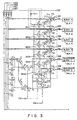
- Figs. 3 is a circuit diagram of a NAND EEPROM having block selecting circuits, taken as an embodiment of the invention.
- This is a circuit in which a respective block selecting circuit is provided in the box drawn with the dotted line in Fig. 3 to make a pair with each block in the circuit of Fig. 2 , shown as prior art, which includes four blocks BLK1-BLK4 having block addresses BA0, BA1, /BA0, /BA1, and two spare redundant blocks SBLK1 and SBLK2.
- Each block selecting circuit is made of an inverter INV1 and corresponding one of circuits BSC1 to BSC6.
- 4-input NAND gates ND1 to ND4 are provided for normally used blocks BLK1 to BLK4, respectively, and 3-input NAND gates ND5 to ND6 are provided for redundant blocks SBLK1 and SBLK2.
- the NAND gates ND1 to ND4 associated with BLK1 to BLK4 are supplied with two block address signals designating individual blocks and a switch signal for switching from the block to a redundant block.
- the NAND gates ND5 and ND6 for the redundant blocks SBLK1 and SBLK2 are supplied with two block address signals designating the respective blocks.
- the NAND gates ND1 to ND6 for BLK1 to BLK4, and for SBLK1 and SBLK2 are supplied with output signals from respective block selecting circuits. The block selecting circuits are explained below in greater detail.
- Fig. 4 is a circuit diagram of an elemental unit of the block selecting circuits according to an embodiment of the invention, Fig. 4 shows one of the BSC circuits coupled to the inverter INV1 in the circuit of Fig. 3.
- the input terminal a is coupled to the common gate input terminal b of a CMOS inverter INV20 via an inverter INV10 on one hand and directly to a gate terminal c of a MOSFET Q10 on the other hand.
- One of the source and drain of the MOSFET Q10 is grounded, and the other of them is coupled to the output point d via a fuse F and further to the output terminal e through an inverter INV30.
- the block selecting circuit operates as follows, where signal voltages at points a, b, c, d and e are labelled V a , V b , V c , V d and V e .
- V d L
- V b H
- V d L
- any appropriate element such as a PROM may be used.
- the MOSFET is any appropriate element capable of supplying "SELECT" signal “H” by changing the signal “H” at point d into “L” when signal "H” is input while the path to point d is held connected.
- a respective block selecting circuit comprising the inverter INV1 and a respective one of the circuits BSC1 to BSC6 is provided for a respective block.
- the inverter INV1 and the gates of the MOSFETs in the circuits BSC1 to BSC6 are supplied with a test mode switch signal, and their output terminals are connected to the NAND gates ND1 to ND6 combined with the respective blocks.
- fuses f a and f d among fuses f a to f d for SBLK1 are blown.
- the externally supplied control signal /CPE is "L"
- the signal /CPE* obtained from /CPE through the buffer is the same logic signal as /CPE.
- /CPE* also becomes "L”.
- RDE becomes "H" when a normally used block is replaced by a spare block.
- the device can be used as a non-defective product.
- the device includes block selecting circuits which never selects a defective block once replaced by a redundant block in the mode for simultaneous writing and simultaneous erasure of all blocks. Therefore, once a defective block is replaced by a redundant block, it never occurs that the voltage boosted by the booster circuit for simultaneous writing and simultaneous erasure of all blocks drops due to leakage of current from the defective block.
- the device can successfully undergo a life test which requires application of a high voltage for simultaneous writing and simultaneous erasure of all blocks, and can be used as a non-defective NAND type EEPROM in all other modes as well.
- each of the block selecting circuits is configured to output the "NON-SELECT" signal when it receives a signal instructing simultaneous writing or simultaneous erasure after the fuse is blown, the voltage for simultaneous writing and simultaneous erasure is never applied to the defective block already replaced by a redundant block.
Landscapes
- For Increasing The Reliability Of Semiconductor Memories (AREA)
- Read Only Memory (AREA)
Claims (3)
- Dispositif de mémoire à semi-conducteur comprenant:dans lequel le dit moyen de commande de sélection contient un nombre de premiers circuits de sélection prévus le long d'un trajet de signal couplant le moyen de désignation et les blocs de mémoire, l'un parmi les premiers circuits de sélection étant prévu pour chacun des blocs de mémoire, chacun des dits premiers circuits de sélection comprenant:un nombre de blocs de mémoire (BLKs 1 à 4), chacun des blocs de mémoire contenant un nombre de cellules de mémoire;un moyen de désignation pour générer un signal de désignation pour désigner l'un parmi les blocs de mémoire à sélectionner en réponse à des signaux d'adresse;au moins un bloc redondant (SBLKs 1, 2) à utiliser à la place d'un bloc de mémoire sélectionné parmi les dits blocs de mémoire;un moyen de commutation (fa à fh) pour générer un signal de commutation pour remplacer le dit bloc de mémoire sélectionné par le dit bloc redondant,le dispositif de mémoire à semi-conducteur étant caractérisé parun moyen de commande de sélection pour empêcher le dit bloc de mémoire sélectionné qui a été remplacé par le dit bloc redondant, d'être sélectionné en réponse à un signal d'entrée de sélection (TST) commandant l'écriture simultanée ou l'effacement simultané de tous les blocs,un premier trajet de signal possédant un nombre de portes logiques pour permettre au signal de désignation de le traverser en direction des blocs de mémoire; etun moyen de blocage du premier trajet de signal pour inverser le signal de désignation passant par les dites portes logiques en réponse au signal d'entrée de sélection (TST), possédant un nombre de premiers inverseurs (INVs 10 - 30) connectés en série, un premier MOSFET (Q10) dont la porte est couplée au signal d'entrée de sélection, et un premier coupe-circuit (f1 - f4) connecté entre les premiers inverseurs et le trajet actuel du premier MOSFET,le moyen de blocage du premier trajet de signal, associé à un bloc non remplacé, commandant le premier MOSFET pour bloquer le signal de sélection passant à travers les dits premiers inverseurs à un potentiel prédéterminé en couplant un point où le dit signal d'entrée de sélection (TST) passant à travers les dits premiers inverseurs apparaít, à un point au dit potentiel prédéterminé.
- Dispositif de mémoire à semi-conducteur selon la revendication 1, dans lequel le dit moyen de blocage du trajet de signal est une PROM.
- Dispositif de mémoire à semi-conducteur selon la revendication 1, dans lequel le moyen de commande de sélection comprend un nombre de seconds circuits de sélection, l'un parmi les seconds circuits de sélection étant prévu pour le bloc redondant qui a été utilisé en place du bloc de mémoire sélectionné, un autre parmi les seconds circuits de sélection étant prévu pour un autre bloc redondant qui n'a pas été utilisé en place du bloc de mémoire sélectionné, au moins le dit second circuit de sélection prévu pour le dit bloc redondant qui n'a pas été utilisé comprenant:un second moyen d'inversion de signal pour inverser le signal de commutation en réponse au signal d'entrée de sélection;un nombre de seconds inverseurs (INVs 10 - 30) connectés en série, un second MOSFET (Q10) couplé au signal d'entrée de sélection, et un second coupe-circuit (f5, f6) connecté entre les seconds inverseurs et le second MOSFET; etun second moyen de blocage du trajet de signal, pour bloquer un troisième trajet de signal entre le dit moyen de commutation et le dit second moyen d'inversion du signal en réponse au signal de commutation, le second moyen de blocage du trajet de signal commandant le second MOSFET en faisant sauter le second coupe-circuit pour mettre le signal de sélection traversant les dits seconds inverseurs à un potentiel prédéterminé en couplant un point où le dit signal de sélection traversant les dits seconds inverseurs apparaít, à un point au dit potentiel prédéterminé, par l'intermédiaire du dit trajet de signal.
Applications Claiming Priority (3)
| Application Number | Priority Date | Filing Date | Title |
|---|---|---|---|
| JP24028994A JP3263259B2 (ja) | 1994-10-04 | 1994-10-04 | 半導体記憶装置 |
| JP24028994 | 1994-10-04 | ||
| JP240289/94 | 1994-10-04 |
Publications (2)
| Publication Number | Publication Date |
|---|---|
| EP0708451A1 EP0708451A1 (fr) | 1996-04-24 |
| EP0708451B1 true EP0708451B1 (fr) | 2002-02-27 |
Family
ID=17057272
Family Applications (1)
| Application Number | Title | Priority Date | Filing Date |
|---|---|---|---|
| EP95115639A Expired - Lifetime EP0708451B1 (fr) | 1994-10-04 | 1995-10-04 | Dispositif de mémoire à semi-conducteurs |
Country Status (7)
| Country | Link |
|---|---|
| US (1) | US5689463A (fr) |
| EP (1) | EP0708451B1 (fr) |
| JP (1) | JP3263259B2 (fr) |
| KR (1) | KR0184086B1 (fr) |
| CN (1) | CN1112707C (fr) |
| DE (1) | DE69525583T2 (fr) |
| MY (1) | MY117283A (fr) |
Cited By (1)
| Publication number | Priority date | Publication date | Assignee | Title |
|---|---|---|---|---|
| EP1564747A1 (fr) * | 2004-02-06 | 2005-08-17 | Sharp Kabushiki Kaisha | Mémoire à sémiconducteur comprenant moyen pour activer simultanément les blocs de mémoire et procédé pour tester le mémoire à sémiconducteur |
Families Citing this family (18)
| Publication number | Priority date | Publication date | Assignee | Title |
|---|---|---|---|---|
| JP3039400B2 (ja) * | 1996-11-21 | 2000-05-08 | 日本電気株式会社 | 不揮発性半導体記憶装置及び不揮発性半導体記憶装置におけるブロック消去のテスト方法 |
| US5831917A (en) * | 1997-06-30 | 1998-11-03 | Vollrath; Joerg | Techniques for reducing redundant element fuses in a dynamic random access memory array |
| US5867433A (en) * | 1997-07-11 | 1999-02-02 | Vanguard International Semiconductor Corporation | Semiconductor memory with a novel column decoder for selecting a redundant array |
| US5886940A (en) * | 1997-08-21 | 1999-03-23 | Micron Technology, Inc. | Self-protected circuit for non-selected programmable elements during programming |
| US5856950A (en) * | 1997-08-22 | 1999-01-05 | Micron Technology, Inc. | Cancellation of redundant elements with a cancel bank |
| JP4413306B2 (ja) | 1999-03-23 | 2010-02-10 | 株式会社東芝 | 半導体記憶装置 |
| JP2002170389A (ja) * | 2000-06-30 | 2002-06-14 | Toshiba Corp | 不揮発性半導体記憶装置とその動作方法 |
| JP4184586B2 (ja) | 2000-09-28 | 2008-11-19 | 株式会社東芝 | 半導体記憶装置 |
| KR100516735B1 (ko) * | 2001-12-08 | 2005-09-22 | 주식회사 하이닉스반도체 | 메모리 셀 어레이 내부 배선을 이용한 로오 엑세스 정보전달 장치 |
| US7336536B2 (en) * | 2004-06-25 | 2008-02-26 | Micron Technology, Inc. | Handling defective memory blocks of NAND memory devices |
| JP4421615B2 (ja) * | 2004-12-24 | 2010-02-24 | スパンション エルエルシー | 記憶装置のバイアス印加方法、および記憶装置 |
| KR100666171B1 (ko) * | 2005-01-10 | 2007-01-09 | 삼성전자주식회사 | 로드 프리 타입의 와이어드 오어 구조를 가지는 불휘발성반도체 메모리 장치와, 이에 대한 구동방법 |
| KR100666170B1 (ko) * | 2005-01-17 | 2007-01-09 | 삼성전자주식회사 | 결함 페이지 버퍼로부터의 데이터 전송이 차단되는와이어드 오어 구조의 불휘발성 반도체 메모리 장치 |
| US7915916B2 (en) * | 2006-06-01 | 2011-03-29 | Micron Technology, Inc. | Antifuse programming circuit with snapback select transistor |
| KR100769772B1 (ko) * | 2006-09-29 | 2007-10-23 | 주식회사 하이닉스반도체 | 플래시 메모리 장치 및 이를 이용한 소거 방법 |
| JP4703624B2 (ja) * | 2007-10-22 | 2011-06-15 | 株式会社東芝 | 半導体記憶装置 |
| JP4985781B2 (ja) * | 2007-11-05 | 2012-07-25 | 富士通株式会社 | 半導体記憶装置およびその制御方法 |
| JP2009146495A (ja) * | 2007-12-13 | 2009-07-02 | Toshiba Corp | Nand型フラッシュメモリ |
Family Cites Families (7)
| Publication number | Priority date | Publication date | Assignee | Title |
|---|---|---|---|---|
| EP0411626B1 (fr) * | 1989-08-04 | 1995-10-25 | Fujitsu Limited | Dispositif de mémoire à semiconducteur à redondance |
| DE69129492T2 (de) * | 1990-10-02 | 1998-11-05 | Toshiba Kawasaki Shi Kk | Halbleiterspeicher |
| JP3019869B2 (ja) * | 1990-10-16 | 2000-03-13 | 富士通株式会社 | 半導体メモリ |
| US5295102A (en) * | 1992-01-31 | 1994-03-15 | Sgs-Thomson Microelectronics, Inc. | Semiconductor memory with improved redundant sense amplifier control |
| JP2869260B2 (ja) * | 1992-08-25 | 1999-03-10 | シャープ株式会社 | 半導体記憶装置 |
| US5428621A (en) * | 1992-09-21 | 1995-06-27 | Sundisk Corporation | Latent defect handling in EEPROM devices |
| US5452251A (en) * | 1992-12-03 | 1995-09-19 | Fujitsu Limited | Semiconductor memory device for selecting and deselecting blocks of word lines |
-
1994
- 1994-10-04 JP JP24028994A patent/JP3263259B2/ja not_active Expired - Fee Related
-
1995
- 1995-10-02 KR KR1019950033643A patent/KR0184086B1/ko not_active Expired - Fee Related
- 1995-10-04 EP EP95115639A patent/EP0708451B1/fr not_active Expired - Lifetime
- 1995-10-04 MY MYPI95002961A patent/MY117283A/en unknown
- 1995-10-04 US US08/539,237 patent/US5689463A/en not_active Expired - Lifetime
- 1995-10-04 DE DE69525583T patent/DE69525583T2/de not_active Expired - Lifetime
- 1995-10-04 CN CN95118648A patent/CN1112707C/zh not_active Expired - Fee Related
Cited By (2)
| Publication number | Priority date | Publication date | Assignee | Title |
|---|---|---|---|---|
| EP1564747A1 (fr) * | 2004-02-06 | 2005-08-17 | Sharp Kabushiki Kaisha | Mémoire à sémiconducteur comprenant moyen pour activer simultanément les blocs de mémoire et procédé pour tester le mémoire à sémiconducteur |
| US7184334B2 (en) | 2004-02-06 | 2007-02-27 | Sharp Kabushiki Kaisha | Semiconductor memory device and method of testing semiconductor memory device |
Also Published As
| Publication number | Publication date |
|---|---|
| JP3263259B2 (ja) | 2002-03-04 |
| EP0708451A1 (fr) | 1996-04-24 |
| DE69525583D1 (de) | 2002-04-04 |
| DE69525583T2 (de) | 2002-10-10 |
| CN1112707C (zh) | 2003-06-25 |
| KR0184086B1 (ko) | 1999-04-15 |
| CN1129338A (zh) | 1996-08-21 |
| US5689463A (en) | 1997-11-18 |
| JPH08106796A (ja) | 1996-04-23 |
| MY117283A (en) | 2004-06-30 |
| KR960015957A (ko) | 1996-05-22 |
Similar Documents
| Publication | Publication Date | Title |
|---|---|---|
| EP0708451B1 (fr) | Dispositif de mémoire à semi-conducteurs | |
| US6646930B2 (en) | Non-volatile semiconductor memory | |
| US4556975A (en) | Programmable redundancy circuit | |
| KR0119888B1 (ko) | 반도체 메모리장치의 결함구제방법 및 그 회로 | |
| US4672240A (en) | Programmable redundancy circuit | |
| US6266792B1 (en) | Semiconductor memory, memory device, and memory card | |
| EP0031380B1 (fr) | Circuit integre a memoire morte programmable avec des modes de controle binaire et de deprogrammation et methodes de programmation et d'essai de ce circuit | |
| US4546454A (en) | Non-volatile memory cell fuse element | |
| KR970010658B1 (ko) | 번-인회로를 가지는 반도체메모리장치 및 그 번-인방법 | |
| US5590075A (en) | Method for testing an electrically erasable and programmable memory device | |
| US5287310A (en) | Memory with I/O mappable redundant columns | |
| US6735727B1 (en) | Flash memory device with a novel redundancy selection circuit and method of using the same | |
| KR960005358B1 (ko) | 반도체 메모리 장치 | |
| JPH03157897A (ja) | 半導体記憶装置の冗長回路 | |
| US5058071A (en) | Semiconductor memory device having means for repairing the memory device with respect to possible defective memory portions | |
| US6101150A (en) | Method and apparatus for using supply voltage for testing in semiconductor memory devices | |
| JP2785936B2 (ja) | 冗長回路のテスト方法 | |
| EP0195412B1 (fr) | Circuit intégré à indicateur de réparation interne incorporé | |
| US5995423A (en) | Method and apparatus for limiting bitline current | |
| US5355338A (en) | Redundancy circuit for semiconductor memory device | |
| KR100502130B1 (ko) | 반도체 기억 장치 및 그 설정 방법 | |
| KR960002011B1 (ko) | 반도체 메모리 장치용 용장 회로 | |
| KR950000342B1 (ko) | 여분 셀 어레이를 갖는 소거 가능 프로그래머블 리드온리 메모리, 및 이 메모리의 스트레스 시험방법 | |
| KR100193445B1 (ko) | 반도체 메모리 장치의 결함 어드레스 판독회로 및 그에 따른 방법 |
Legal Events
| Date | Code | Title | Description |
|---|---|---|---|
| PUAI | Public reference made under article 153(3) epc to a published international application that has entered the european phase |
Free format text: ORIGINAL CODE: 0009012 |
|
| 17P | Request for examination filed |
Effective date: 19951004 |
|
| AK | Designated contracting states |
Kind code of ref document: A1 Designated state(s): DE FR GB |
|
| 17Q | First examination report despatched |
Effective date: 19990707 |
|
| GRAG | Despatch of communication of intention to grant |
Free format text: ORIGINAL CODE: EPIDOS AGRA |
|
| GRAG | Despatch of communication of intention to grant |
Free format text: ORIGINAL CODE: EPIDOS AGRA |
|
| GRAH | Despatch of communication of intention to grant a patent |
Free format text: ORIGINAL CODE: EPIDOS IGRA |
|
| GRAH | Despatch of communication of intention to grant a patent |
Free format text: ORIGINAL CODE: EPIDOS IGRA |
|
| REG | Reference to a national code |
Ref country code: GB Ref legal event code: IF02 |
|
| GRAA | (expected) grant |
Free format text: ORIGINAL CODE: 0009210 |
|
| AK | Designated contracting states |
Kind code of ref document: B1 Designated state(s): DE FR GB |
|
| PG25 | Lapsed in a contracting state [announced via postgrant information from national office to epo] |
Ref country code: FR Free format text: LAPSE BECAUSE OF FAILURE TO SUBMIT A TRANSLATION OF THE DESCRIPTION OR TO PAY THE FEE WITHIN THE PRESCRIBED TIME-LIMIT Effective date: 20020227 |
|
| REF | Corresponds to: |
Ref document number: 69525583 Country of ref document: DE Date of ref document: 20020404 |
|
| EN | Fr: translation not filed | ||
| PLBE | No opposition filed within time limit |
Free format text: ORIGINAL CODE: 0009261 |
|
| STAA | Information on the status of an ep patent application or granted ep patent |
Free format text: STATUS: NO OPPOSITION FILED WITHIN TIME LIMIT |
|
| 26N | No opposition filed |
Effective date: 20021128 |
|
| PGFP | Annual fee paid to national office [announced via postgrant information from national office to epo] |
Ref country code: GB Payment date: 20110928 Year of fee payment: 17 |
|
| PGFP | Annual fee paid to national office [announced via postgrant information from national office to epo] |
Ref country code: DE Payment date: 20120927 Year of fee payment: 18 |
|
| GBPC | Gb: european patent ceased through non-payment of renewal fee |
Effective date: 20121004 |
|
| PG25 | Lapsed in a contracting state [announced via postgrant information from national office to epo] |
Ref country code: GB Free format text: LAPSE BECAUSE OF NON-PAYMENT OF DUE FEES Effective date: 20121004 |
|
| REG | Reference to a national code |
Ref country code: DE Ref legal event code: R119 Ref document number: 69525583 Country of ref document: DE Effective date: 20140501 |
|
| PG25 | Lapsed in a contracting state [announced via postgrant information from national office to epo] |
Ref country code: DE Free format text: LAPSE BECAUSE OF NON-PAYMENT OF DUE FEES Effective date: 20140501 |