EP0708486B1 - Transistor semi-conducteur à effet de champ à région étendue en contact avec le substrat - Google Patents
Transistor semi-conducteur à effet de champ à région étendue en contact avec le substrat Download PDFInfo
- Publication number
- EP0708486B1 EP0708486B1 EP95116348A EP95116348A EP0708486B1 EP 0708486 B1 EP0708486 B1 EP 0708486B1 EP 95116348 A EP95116348 A EP 95116348A EP 95116348 A EP95116348 A EP 95116348A EP 0708486 B1 EP0708486 B1 EP 0708486B1
- Authority
- EP
- European Patent Office
- Prior art keywords
- region
- semiconductor substrate
- substrate
- conductivity type
- substrate contact
- Prior art date
- Legal status (The legal status is an assumption and is not a legal conclusion. Google has not performed a legal analysis and makes no representation as to the accuracy of the status listed.)
- Expired - Lifetime
Links
Images




Classifications
-
- H—ELECTRICITY
- H10—SEMICONDUCTOR DEVICES; ELECTRIC SOLID-STATE DEVICES NOT OTHERWISE PROVIDED FOR
- H10D—INORGANIC ELECTRIC SEMICONDUCTOR DEVICES
- H10D84/00—Integrated devices formed in or on semiconductor substrates that comprise only semiconducting layers, e.g. on Si wafers or on GaAs-on-Si wafers
-
- H—ELECTRICITY
- H10—SEMICONDUCTOR DEVICES; ELECTRIC SOLID-STATE DEVICES NOT OTHERWISE PROVIDED FOR
- H10D—INORGANIC ELECTRIC SEMICONDUCTOR DEVICES
- H10D64/00—Electrodes of devices having potential barriers
- H10D64/20—Electrodes characterised by their shapes, relative sizes or dispositions
- H10D64/23—Electrodes carrying the current to be rectified, amplified, oscillated or switched, e.g. sources, drains, anodes or cathodes
- H10D64/251—Source or drain electrodes for field-effect devices
- H10D64/257—Source or drain electrodes for field-effect devices for lateral devices wherein the source or drain electrodes are characterised by top-view geometrical layouts, e.g. interdigitated, semi-circular, annular or L-shaped electrodes
-
- H—ELECTRICITY
- H10—SEMICONDUCTOR DEVICES; ELECTRIC SOLID-STATE DEVICES NOT OTHERWISE PROVIDED FOR
- H10D—INORGANIC ELECTRIC SEMICONDUCTOR DEVICES
- H10D62/00—Semiconductor bodies, or regions thereof, of devices having potential barriers
- H10D62/10—Shapes, relative sizes or dispositions of the regions of the semiconductor bodies; Shapes of the semiconductor bodies
- H10D62/102—Constructional design considerations for preventing surface leakage or controlling electric field concentration
- H10D62/112—Constructional design considerations for preventing surface leakage or controlling electric field concentration for preventing surface leakage due to surface inversion layers, e.g. by using channel stoppers
-
- H—ELECTRICITY
- H10—SEMICONDUCTOR DEVICES; ELECTRIC SOLID-STATE DEVICES NOT OTHERWISE PROVIDED FOR
- H10D—INORGANIC ELECTRIC SEMICONDUCTOR DEVICES
- H10D62/00—Semiconductor bodies, or regions thereof, of devices having potential barriers
- H10D62/10—Shapes, relative sizes or dispositions of the regions of the semiconductor bodies; Shapes of the semiconductor bodies
- H10D62/17—Semiconductor regions connected to electrodes not carrying current to be rectified, amplified or switched, e.g. channel regions
- H10D62/351—Substrate regions of field-effect devices
- H10D62/357—Substrate regions of field-effect devices of FETs
- H10D62/364—Substrate regions of field-effect devices of FETs of IGFETs
-
- H—ELECTRICITY
- H10—SEMICONDUCTOR DEVICES; ELECTRIC SOLID-STATE DEVICES NOT OTHERWISE PROVIDED FOR
- H10D—INORGANIC ELECTRIC SEMICONDUCTOR DEVICES
- H10D62/00—Semiconductor bodies, or regions thereof, of devices having potential barriers
- H10D62/10—Shapes, relative sizes or dispositions of the regions of the semiconductor bodies; Shapes of the semiconductor bodies
- H10D62/17—Semiconductor regions connected to electrodes not carrying current to be rectified, amplified or switched, e.g. channel regions
- H10D62/351—Substrate regions of field-effect devices
- H10D62/357—Substrate regions of field-effect devices of FETs
- H10D62/364—Substrate regions of field-effect devices of FETs of IGFETs
- H10D62/378—Contact regions to the substrate regions
-
- H—ELECTRICITY
- H10—SEMICONDUCTOR DEVICES; ELECTRIC SOLID-STATE DEVICES NOT OTHERWISE PROVIDED FOR
- H10D—INORGANIC ELECTRIC SEMICONDUCTOR DEVICES
- H10D89/00—Aspects of integrated devices not covered by groups H10D84/00 - H10D88/00
Definitions
- the present invention relates to a metal oxide semiconductor (MOS)-type semiconductor device, and more particularly, to a low substrate noise MOS-type semiconductor device.
- MOS metal oxide semiconductor
- the noise from the digital circuits via the power supply lines to the analog circuits can be reduced by providing individual power supply lines for the digital circuits and the analog circuits, an approach which has been broadly used.
- the noise, so called substrate noise, from the digital circuits via the substrate to the analog circuits is generated from a 1-bit output delta-sigma modulator or a charge pump circuit of a phase locked loop (PLL) circuit.
- PLL phase locked loop
- CMOS device if an N-channel MOS transistor is formed in a P-type semiconductor substrate, a P-channel MOS transistor is formed in an N-type well.
- the back gate of the N-channel MOS transistor is the substrate, and the back gate of the P-channel Mos transistor is the well. Since the well is separated from the substrate by a PN junction therebetween and an analog power supply voltage is applied to the well, the P-channel MOS transistor hardly suffers from the substrate noise. Conversely, the N-channel MOS transistor suffers directly from the substrate noise.
- an impurity diffusion region i.e., a substrate contact region, of the same conductivity type as the substrate having a higher impurity concentration than the substrate is formed in the substrate to surround a transistor area. Also, the substrate contact region is connected to a definite power supply voltage line. Thus, the voltage in the substrate around the transistor area is brought close to the voltage at the power supply voltage line, thus reducing the substrate noise. This will be explained later in detail.
- the devices have become increased in size, thus increasing the substrate noise and reducing the impedance of noise sources, so that the power supply line connected to the substrate contact region per se suffers from the substrate noise. Also, this power supply line serves as a noise source for other transistor areas. Further, since individual power supply voltages are applied to the source region and the substrate contact region, noises superimposed onto the power supply voltages are added to a current of the transistor as a noise current.
- the width of the substrate contact region is so reduced that the resistance of the substrate contact region and its neighborhood is increased.
- the resistance between the back gate and the substrate contact region is not so small as the resistance between the back gate and the substrate, and accordingly, the substrate noise can be reduced by the substrate contact region to less than 1/2.
- a channel stopper region is provided to surround the substrate contact region, to thus avoid the creation of a parasitic MOS transistor.
- the substrate contact region serves as a low impedance for noise transmitted via the channel stopper, the substrate noise cannot be further suppressed.
- EP-A-0 294 868 discloses a semiconductor device comprising a silicon layer of a first conductivity type, which is disposed on a dielectric substrate and in which at least two zones of a semiconductor circuit element of a second opposite conductivity type and a contact zone having the same conductivity type as, but a higher doping concentration than the silicon layer are provided, which zones adjoin a surface of the silicon layer.
- the contact zone extends below the zones of the field effect transistor.
- MOS-type semiconductor device as defined by claim 1 and claim 7 is provided.
- FIG. 1 is a cross-sectional view of Fig. 1.
- a relatively thick field silicon oxide layer 2 having a P + -type channel stopper 2a therebeneath is formed on a P - -type monocrystalline silicon substrate 1 to partition an active area A1 and a field area A2 to isolate the active area A1 from other active areas. Also, a transistor area T is defined within the active area A1.
- N + -type impurity diffusion regions 3-1 to 3-5 ara formed within the substrate 1.
- the regions 3-2 and 3-4 serve as drain regions
- the regions 3-1, 3-3 and 3-5 serve as source regions.
- drain electrodes 4-1 and 4-2 which form a multi-finger type drain configuration.
- source electrodes 5-1, 5-2 and 5-3 which form a multi-finger type source configuration.
- gate electrodes 6-1, 6-2, 6-3, 6-4 and 6-5 which form a multi-finger configuration.
- P + -type substrate contact regions 7-1 and 7-2 are provided in the semiconductor substrate 1 to surround the transistor area T, i.e., the N + -type impurity regions 3-1 to 3-5.
- reference numerals 8-1 and 8-2 designate power supply lines for applying a definite voltage to the substrate contact regions 7-1 and 7-2.
- reference numeral 9 designates an insulating layer made of silicon oxide.
- the power supply lines 8-1 and 8-2 connected to the substrate contact regions 7-1 and 7-2 per se suffer from the substrate noise. Also, this power supply lines 8-1 and 8-2 serve as noise sources for other transistor areas. Further, since individual power supply voltages are applied to the sources regions 3-1, 3-3 and 3-5 and the substrate contact regions 7-1 and 7-2, noises superimposed onto the power supply voltages are added to a current of the transistor as a noise current.
- the width of the substrate contact region is reduced. Since the substrate contact resistance is determined by the spreading resistance effect, the resistance of the substrate contact regions 7-1 and 7-2 and its neighborhood is drastically increased. As a result, the resistance R 1 between an imaginary summing node N 1 and the substrate contact region 7-1 (7-2) is not as small as the resistance R 0 between the imaginary summing node N 1 and the substrate. For example, the resistance R 1 is larger than hundreds of ⁇ , and the resistance R 0 is hundreds of ⁇ .
- the channel stopper region 2a is provided to surround the substrate contact regions 7-1 and 7-2, to thus avoid the creation of a parasitic MOS transistor.
- the substrate contact regions 7-1 and 7-2 serve as a low impedance for noise transmitted via the channel stopper 2a, the substrate noise cannot be further suppressed.
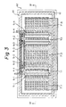
- Figs. 3 and 4 illustrate an embodiment of the present invention. Note that Fig. 4 is a cross-sectional view taken along the line IV - IV of Fig. 3.
- each of the transistor areas T1 and T2 includes one drain region 3-2 (3-4) connected to the drain electrodes 4-1 (4-2), two source regions 3-1 and 3-3 (3-3' and 3-5), and two gate electrodes 6-1 and 6-2 (6-3 and 6-4).
- P + -type substrate contact regions 7'-1, 7'-2 and 7'-3 are provided on sides of the transistor areas T1 and T2, i.e., adjacent to the source regions 3-1, 3-3, 3-3' and 3-5.
- the substrate contact regions 7'-1, 7'-2 and 7'-3 are wider than the substrate contact regions 7-1 and 7-2 of Fig. 2.
- the width of each of the substrate contact regions 7'-1, 7'-2 and 7'-3 is larger than half of intervals thereof.
- the substrate contact regions 7'-1, 7'-2 and 7'-3 are electrically connected to the source regions 3-1, 3-3 (3-3') and 3-5, respectively, by source electrodes 5'-1, 5'-2 and 5'-3.
- the resistance (R 1 ' + R 2 ) between the back gate and the substrate contact region 7'-1 (7'-2, 7'-3) can be reduced.
- the resistance R 1 ' can be reduced by about one tenth of the resistance R 1 of Fig. 2.
- the power supply noise mainly depends upon the source noise, thus reducing a load of design.
- an N + -type impurity region 10 is provided to surround the transistor areas T1 and T2.
- the N + -type impurity region 10 is deeper than the drain source regions 3-1, 3-3, 3-3' and 3-5 and the drain regions 3-2 and 3-4.
- the N + -type impurity region 10 is in a floating state; however, the N + -type impurity region 10 can be connected to a definite power supply line via an electrode 11 as illustrated in Fig. 5. Therefore, the N + -type impurity region 10 serves as a high impedance as indicated by R 3 for low frequency (less than hundreds of kHz) noise transmitted via the channel stopper 2a, the substrate noise can be further reduced.
- the resistance between a back gate and the substrate contact regions can be reduced, and accordingly, the substrate noise can be reduced.
Landscapes
- Insulated Gate Type Field-Effect Transistor (AREA)
- Metal-Oxide And Bipolar Metal-Oxide Semiconductor Integrated Circuits (AREA)
- Element Separation (AREA)
Claims (12)
- Dispositif à semi-conducteur, comprenant :caractérisé parun substrat semi-conducteur (1) ayant un premier type de conductivité ;une zone de drain (3-2, 3-4) ayant un second type de conductivité opposé audit premier type de conductivité, formée dans ledit substrat semi-conducteur ;une zone de source (3-1, 3-3, 3-3', 3-5) ayant ledit second type de conductivité, formée dans ledit substrat semi-conducteur ;une électrode de grille (6-1 - 6-4), formée par dessus ledit substrat semi-conducteur, entre ladite zone de drain et ladite zone de source ;une zone de contact de substrat (7'-1 - 7'-3) ayant ledit premier type de conductivité et ayant une concentration en impuretés supérieure à celle dudit substrat semi-conducteur, ladite zone de contact de substrat étant formée dans ledit substrat semi-conducteur en étant adjacente à ladite zone de source ;une électrode de source (5'-1 ∼ 5'-3) formée sur ladite zone de source ; etune électrode de drain (4-1 - 4-3) formée sur ladite zone de drain,ladite zone de drain, ladite zone de source et ladite zone de contact de substrat étant agencées suivant une direction, la largeur de ladite zone de contact de substrat le long de ladite direction étant supérieure à la largeur de ladite zone de drain le long de cette direction et à la largeur de ladite zone de source le long de ladite direction ;
une zone de diffusion d'impuretés (10) ayant ledit second type de conductivité, qui est formée dans ledit substrat semi-conducteur et qui entoure ladite zone de source, ladite zone de drain et ladite zone de contact de substrat. - Dispositif selon la revendication 1, dans lequel ladite électrode de source est électriquement connectée à ladite zone de contact de substrat.
- Dispositif selon la revendication 1, dans lequel ladite zone de diffusion d'impuretés est plus profonde que ladite zone de source, ladite zone de drain et ladite zone de contact de substrat.
- Dispositif selon la revendication 1, dans lequel ladite zone de diffusion d'impuretés est connectée à une ligne de tension d'alimentation définie (11), de sorte qu'une tension de polarisation inverse est appliquée entre ladite zone de diffusion d'impuretés et ledit substrat semi-conducteur.
- Dispositif selon la revendication 1, dans lequel ladite zone de diffusion d'impuretés est dans un état flottant.
- Dispositif selon la revendication 1, comprenant, en outre, une zone d'arrêt de canal (2a) ayant ledit premier type de conductivité, qui est formée dans ledit substrat semi-conducteur et qui entoure ladite zone de diffusion d'impuretés.
- Dispositif à semi-conducteur comportant une pluralité d'aires de transistor d'un transistor MOS, comprenant :un substrat semi-conducteur (1) ayant un premier type de conductivité ;une pluralité de zones de drain (3-2, 3-4) ayant un second type de conductivité opposé audit premier type de conductivité, chacune desdites zones de drain étant formée dans l'une desdites aires de transistor dudit substrat semi-conducteur ;une pluralité de paires de zones de source (3-1, 3-3, 3-3', 3-5) ayant ledit second type de conductivité, chacune desdites paires de zones de source étant formée dans l'une desdites aires de transistor dudit substrat semi-conducteur et entourant l'une, respective, desdites zones de drain ;une pluralité de paires d'électrodes de grille (6-1, 6-2, 6-3, 6-4), chacune desdites paires d'électrodes de grille étant formée par dessus l'une desdites aires de transistor dudit substrat semi-conducteur, entre l'une, respective, desdites zones de drain et l'une, respective, desdites paires de zones de source ;une pluralité de zones de contact de substrat (7'-1, 7'-2, 7'-3) ayant ledit premier type de conductivité et ayant une concentration en impuretés supérieure à celle dudit substrat semi-conducteur, lesdites zones de contact de substrat étant formées dans ledit substrat semi-conducteur en étant adjacentes auxdites paires de zones de source ;une électrode de source (5'-1, 5'-2, 5'-3) formée par dessus lesdites paires de zones de source ; etune électrode de drain (4-1, 4-2) formée sur lesdites zones de drain,lesdites zones de drain, lesdites paires de zones de source et lesdites zones de contact de substrat étant agencées suivant une direction, la largeur de chacune desdites zones de contact de substrat suivant ladite direction étant supérieure à la moitié des intervalles desdites zones de contact de substrat le long de ladite directionledit dispositif comprenant, en outre, une zone de diffusion d'impuretés (10) ayant ledit second type de conductivité, qui est formée dans ledit substrat semi-conducteur et qui entoure lesdites aires de transistor.
- Dispositif selon la revendication 7, dans lequel ladite électrode de source est connectée auxdites zones de contact de substrat,
- Dispositif selon la revendication 7, dans lequel ladite zone de diffusion d'impuretés est plus profonde que lesdites zones de drain.
- Dispositif selon la revendication 7, dans lequel ladite zone de diffusion d'impuretés est connectée à une ligne de tension d'alimentation définie (11), de sorte qu'une tension de polarisation inverse est appliquée entre ladite zone de diffusion d'impuretés et ledit substrat semi-conducteur.
- Dispositif selon la revendication 7, dans lequel ladite zone de diffusion d'impuretés est dans un état flottant.
- Dispositif selon la revendication 7, comprenant, en outre, une zone d'arrêt de canal (2a) ayant ledit premier type de conductivité, qui est formée dans ledit substrat semi-conducteur et qui entoure ladite zone de diffusion d'impuretés.
Applications Claiming Priority (3)
| Application Number | Priority Date | Filing Date | Title |
|---|---|---|---|
| JP25085394 | 1994-10-17 | ||
| JP250853/94 | 1994-10-17 | ||
| JP6250853A JPH08115985A (ja) | 1994-10-17 | 1994-10-17 | 低雑音の半導体集積回路 |
Publications (3)
| Publication Number | Publication Date |
|---|---|
| EP0708486A2 EP0708486A2 (fr) | 1996-04-24 |
| EP0708486A3 EP0708486A3 (fr) | 1997-07-02 |
| EP0708486B1 true EP0708486B1 (fr) | 2001-09-12 |
Family
ID=17213986
Family Applications (1)
| Application Number | Title | Priority Date | Filing Date |
|---|---|---|---|
| EP95116348A Expired - Lifetime EP0708486B1 (fr) | 1994-10-17 | 1995-10-17 | Transistor semi-conducteur à effet de champ à région étendue en contact avec le substrat |
Country Status (5)
| Country | Link |
|---|---|
| US (1) | US5559356A (fr) |
| EP (1) | EP0708486B1 (fr) |
| JP (1) | JPH08115985A (fr) |
| KR (1) | KR100196734B1 (fr) |
| DE (1) | DE69522634T2 (fr) |
Families Citing this family (7)
| Publication number | Priority date | Publication date | Assignee | Title |
|---|---|---|---|---|
| JPH09199607A (ja) * | 1996-01-18 | 1997-07-31 | Nec Corp | Cmos半導体装置 |
| US6507235B1 (en) * | 1996-06-18 | 2003-01-14 | Micron Technology, Inc. | Local substrate pumping in integrated circuits |
| JP2003017704A (ja) | 2001-06-29 | 2003-01-17 | Denso Corp | 半導体装置 |
| JP2006228942A (ja) * | 2005-02-17 | 2006-08-31 | Nec Electronics Corp | 半導体装置 |
| JP2008233123A (ja) | 2007-03-16 | 2008-10-02 | Sony Corp | 表示装置 |
| US10410957B2 (en) * | 2016-03-31 | 2019-09-10 | Skyworks Solutions, Inc. | Body contacts for field-effect transistors |
| WO2021251081A1 (fr) * | 2020-06-08 | 2021-12-16 | ローム株式会社 | Dispositif à semi-conducteur et appareil électronique |
Family Cites Families (11)
| Publication number | Priority date | Publication date | Assignee | Title |
|---|---|---|---|---|
| JPS60140862A (ja) * | 1983-12-28 | 1985-07-25 | Nec Corp | 半導体記憶装置 |
| JPS61148862A (ja) * | 1984-12-22 | 1986-07-07 | Agency Of Ind Science & Technol | 半導体装置 |
| JPS61179563A (ja) * | 1985-02-04 | 1986-08-12 | Toshiba Corp | 相補型集積回路装置 |
| JPS62105525A (ja) * | 1985-11-01 | 1987-05-16 | Hitachi Ltd | 半導体集積回路装置 |
| NL8701251A (nl) * | 1987-05-26 | 1988-12-16 | Philips Nv | Halfgeleiderinrichting en werkwijze ter vervaardiging daarvan. |
| JP2926969B2 (ja) * | 1990-04-26 | 1999-07-28 | 富士電機株式会社 | Mis型電界効果トランジスタを有する半導体装置 |
| KR950009893B1 (ko) * | 1990-06-28 | 1995-09-01 | 미쓰비시 뎅끼 가부시끼가이샤 | 반도체기억장치 |
| JP2609753B2 (ja) * | 1990-10-17 | 1997-05-14 | 株式会社東芝 | 半導体装置 |
| EP0601823B1 (fr) * | 1992-12-09 | 2000-10-11 | Compaq Computer Corporation | Méthode de fabrication d'un transistor à effet de champ avec verrouillage sous forme de diode schottky intégrée |
| JP2850736B2 (ja) * | 1992-12-28 | 1999-01-27 | 松下電器産業株式会社 | 半導体装置 |
| US5451799A (en) * | 1992-12-28 | 1995-09-19 | Matsushita Electric Industrial Co., Ltd. | MOS transistor for protection against electrostatic discharge |
-
1994
- 1994-10-17 JP JP6250853A patent/JPH08115985A/ja active Pending
-
1995
- 1995-10-16 US US08/543,285 patent/US5559356A/en not_active Expired - Lifetime
- 1995-10-17 KR KR1019950035840A patent/KR100196734B1/ko not_active Expired - Fee Related
- 1995-10-17 EP EP95116348A patent/EP0708486B1/fr not_active Expired - Lifetime
- 1995-10-17 DE DE69522634T patent/DE69522634T2/de not_active Expired - Fee Related
Also Published As
| Publication number | Publication date |
|---|---|
| DE69522634D1 (de) | 2001-10-18 |
| KR960015896A (ko) | 1996-05-22 |
| EP0708486A3 (fr) | 1997-07-02 |
| US5559356A (en) | 1996-09-24 |
| KR100196734B1 (ko) | 1999-06-15 |
| DE69522634T2 (de) | 2002-07-04 |
| JPH08115985A (ja) | 1996-05-07 |
| EP0708486A2 (fr) | 1996-04-24 |
Similar Documents
| Publication | Publication Date | Title |
|---|---|---|
| US4994886A (en) | Composite MOS transistor and application to a free-wheel diode | |
| KR20010015835A (ko) | 반도체 장치 | |
| JP2001102586A (ja) | 高耐圧半導体装置 | |
| US5604655A (en) | Semiconductor protection circuit and semiconductor protection device | |
| JPH0821680B2 (ja) | 集積回路 | |
| JP2528794B2 (ja) | ラツチアツプ保護回路付き集積回路 | |
| HK79493A (en) | Integrated circuit of the complementary technique having a substrate bias generator | |
| JP2954854B2 (ja) | 集積回路チップ | |
| US5608238A (en) | Semiconductor device having two insulated gates and capable of thyristor function and method for operating the same | |
| US7816212B2 (en) | Method of high voltage operation of a field effect transistor | |
| US4969020A (en) | Semiconductor device | |
| US5559356A (en) | Semiconductor device with large substrate contact region | |
| JPS6050066B2 (ja) | Mos半導体集積回路装置 | |
| US4476479A (en) | Semiconductor device with operating voltage coupling region | |
| JP2825038B2 (ja) | 半導体装置 | |
| KR100867572B1 (ko) | 고전압 섬 영역 내에 바이폴라 트랜지스터가 내장된고전압 집적 회로 | |
| HK59996A (en) | Integrated circuit with anti-''latch-up'' circuit obtained using complementary mos circuit technology | |
| JPH03248554A (ja) | Cmos半導体集積回路装置 | |
| US4680605A (en) | High voltage depletion mode transistor with serpentine current path | |
| US5880514A (en) | Protection circuit for semiconductor device | |
| US4952998A (en) | Integrated circuit with complementary MOS transistors | |
| JPS6230704B2 (fr) | ||
| JPH088359B2 (ja) | 半導体装置 | |
| JPS5931864B2 (ja) | 相補型絶縁ゲ−ト半導体回路 | |
| JP2553600B2 (ja) | BiMOS半導体集積回路 |
Legal Events
| Date | Code | Title | Description |
|---|---|---|---|
| PUAI | Public reference made under article 153(3) epc to a published international application that has entered the european phase |
Free format text: ORIGINAL CODE: 0009012 |
|
| AK | Designated contracting states |
Kind code of ref document: A2 Designated state(s): DE FR GB NL |
|
| PUAL | Search report despatched |
Free format text: ORIGINAL CODE: 0009013 |
|
| AK | Designated contracting states |
Kind code of ref document: A3 Designated state(s): DE FR GB NL |
|
| 17P | Request for examination filed |
Effective date: 19971105 |
|
| 17Q | First examination report despatched |
Effective date: 19980210 |
|
| GRAG | Despatch of communication of intention to grant |
Free format text: ORIGINAL CODE: EPIDOS AGRA |
|
| GRAG | Despatch of communication of intention to grant |
Free format text: ORIGINAL CODE: EPIDOS AGRA |
|
| GRAH | Despatch of communication of intention to grant a patent |
Free format text: ORIGINAL CODE: EPIDOS IGRA |
|
| GRAH | Despatch of communication of intention to grant a patent |
Free format text: ORIGINAL CODE: EPIDOS IGRA |
|
| GRAA | (expected) grant |
Free format text: ORIGINAL CODE: 0009210 |
|
| AK | Designated contracting states |
Kind code of ref document: B1 Designated state(s): DE FR GB NL |
|
| REF | Corresponds to: |
Ref document number: 69522634 Country of ref document: DE Date of ref document: 20011018 |
|
| PGFP | Annual fee paid to national office [announced via postgrant information from national office to epo] |
Ref country code: NL Payment date: 20011031 Year of fee payment: 7 |
|
| REG | Reference to a national code |
Ref country code: GB Ref legal event code: IF02 |
|
| ET | Fr: translation filed | ||
| PLBE | No opposition filed within time limit |
Free format text: ORIGINAL CODE: 0009261 |
|
| STAA | Information on the status of an ep patent application or granted ep patent |
Free format text: STATUS: NO OPPOSITION FILED WITHIN TIME LIMIT |
|
| 26N | No opposition filed | ||
| REG | Reference to a national code |
Ref country code: GB Ref legal event code: 732E |
|
| PG25 | Lapsed in a contracting state [announced via postgrant information from national office to epo] |
Ref country code: NL Free format text: LAPSE BECAUSE OF NON-PAYMENT OF DUE FEES Effective date: 20030501 |
|
| NLV4 | Nl: lapsed or anulled due to non-payment of the annual fee |
Effective date: 20030501 |
|
| REG | Reference to a national code |
Ref country code: FR Ref legal event code: TP |
|
| PGFP | Annual fee paid to national office [announced via postgrant information from national office to epo] |
Ref country code: DE Payment date: 20081014 Year of fee payment: 14 |
|
| PGFP | Annual fee paid to national office [announced via postgrant information from national office to epo] |
Ref country code: GB Payment date: 20081015 Year of fee payment: 14 |
|
| PG25 | Lapsed in a contracting state [announced via postgrant information from national office to epo] |
Ref country code: DE Free format text: LAPSE BECAUSE OF NON-PAYMENT OF DUE FEES Effective date: 20100501 |
|
| REG | Reference to a national code |
Ref country code: FR Ref legal event code: CD |
|
| PG25 | Lapsed in a contracting state [announced via postgrant information from national office to epo] |
Ref country code: GB Free format text: LAPSE BECAUSE OF NON-PAYMENT OF DUE FEES Effective date: 20091017 |
|
| PGFP | Annual fee paid to national office [announced via postgrant information from national office to epo] |
Ref country code: FR Payment date: 20141008 Year of fee payment: 20 |