EP0708515A1 - Circuit de protection pour la protection d'une charge contre une tension d'entrée trop élevée - Google Patents
Circuit de protection pour la protection d'une charge contre une tension d'entrée trop élevée Download PDFInfo
- Publication number
- EP0708515A1 EP0708515A1 EP95116302A EP95116302A EP0708515A1 EP 0708515 A1 EP0708515 A1 EP 0708515A1 EP 95116302 A EP95116302 A EP 95116302A EP 95116302 A EP95116302 A EP 95116302A EP 0708515 A1 EP0708515 A1 EP 0708515A1
- Authority
- EP
- European Patent Office
- Prior art keywords
- depletion mode
- mode mosfet
- mosfet
- gate
- voltage
- Prior art date
- Legal status (The legal status is an assumption and is not a legal conclusion. Google has not performed a legal analysis and makes no representation as to the accuracy of the status listed.)
- Granted
Links
Images


Classifications
-
- H—ELECTRICITY
- H02—GENERATION; CONVERSION OR DISTRIBUTION OF ELECTRIC POWER
- H02H—EMERGENCY PROTECTIVE CIRCUIT ARRANGEMENTS
- H02H9/00—Emergency protective circuit arrangements for limiting excess current or voltage without disconnection
- H02H9/04—Emergency protective circuit arrangements for limiting excess current or voltage without disconnection responsive to excess voltage
- H02H9/042—Emergency protective circuit arrangements for limiting excess current or voltage without disconnection responsive to excess voltage comprising means to limit the absorbed power or indicate damaged over-voltage protection device
-
- H—ELECTRICITY
- H02—GENERATION; CONVERSION OR DISTRIBUTION OF ELECTRIC POWER
- H02J—ELECTRIC POWER NETWORKS; CIRCUIT ARRANGEMENTS OR SYSTEMS FOR SUPPLYING OR DISTRIBUTING ELECTRIC POWER; SYSTEMS FOR STORING ELECTRIC ENERGY
- H02J7/00—Circuit arrangements for charging or discharging batteries or for supplying loads from batteries
- H02J7/60—Circuit arrangements for charging or discharging batteries or for supplying loads from batteries including safety or protection arrangements
- H02J7/64—Circuit arrangements for charging or discharging batteries or for supplying loads from batteries including safety or protection arrangements against overvoltage
-
- H—ELECTRICITY
- H02—GENERATION; CONVERSION OR DISTRIBUTION OF ELECTRIC POWER
- H02J—ELECTRIC POWER NETWORKS; CIRCUIT ARRANGEMENTS OR SYSTEMS FOR SUPPLYING OR DISTRIBUTING ELECTRIC POWER; SYSTEMS FOR STORING ELECTRIC ENERGY
- H02J7/00—Circuit arrangements for charging or discharging batteries or for supplying loads from batteries
- H02J7/60—Circuit arrangements for charging or discharging batteries or for supplying loads from batteries including safety or protection arrangements
- H02J7/663—Circuit arrangements for charging or discharging batteries or for supplying loads from batteries including safety or protection arrangements using battery or load disconnect circuits
Definitions
- This invention relates to circuitry for protecting a load, particularly a load containing semiconductor devices, from excessive or reversed voltages.
- this invention relates to circuitry for protecting a load from a condition sometimes referred to as "load dump", which occurs in automobiles.
- Semiconductor devices can be severely damaged if they are exposed to a "reversed voltage" such as occurs, for example, when a negative voltage is applied to a terminal which is designed to receive a positive voltage. This can occur in an automobile when the battery is inadvertently connected with its terminals reversed. In the presence of a reversed voltage condition, PN junctions within a semiconductor device may become forward biased, resulting in large currents, overheating, melting of aluminum traces and permanent damage to the device.
- a reversed voltage such as occurs, for example, when a negative voltage is applied to a terminal which is designed to receive a positive voltage. This can occur in an automobile when the battery is inadvertently connected with its terminals reversed. In the presence of a reversed voltage condition, PN junctions within a semiconductor device may become forward biased, resulting in large currents, overheating, melting of aluminum traces and permanent damage to the device.
- a Schottky diode in series with the load, as shown in Figs. 1A and 1B.
- Diode 10 represents a PN junction within module 11.
- Schottky diode 12 becomes reverse-biased and prevents the current from flowing, thereby protecting the module 11.
- Schottky diode 12 is forward biased and dissipates a small amount of power.
- a power MOSFET and special control circuit can be used to provide protection against a reversed battery, as described in U.S. Application Ser. No. 08/067,373, which is incorporated herein by reference. While from a technical standpoint this is an attractive solution to the problem, the inclusion of a power MOSFET in the circuit represents an added cost.
- Load dump typically occurs when the generator, running at full current to charge the battery, is momentarily disconnected from the battery post by a mechanical vibration or shock.
- the resulting open circuit, represented by switch 20 in Fig. 2A, causes a rapid decrease in the current flowing through various inductances in the circuitry, represented as 21 and 22.
- the generator itself also includes inductive elements.
- V L dI/dt , very high voltages, on the order of hundreds of volts, can be created in this way. Such voltages would destroy most ICs.
- a zener diode 23 frequently known as a transorb, is connected in parallel with the load, which is designated as 24 in Fig. 2A.
- Zener diode 23 is normally used to clamp the voltage to 30 volts or so. In practice, however, it takes tens of nanoseconds for zener diode 23 to fire, during which time the voltage on the supply line may soar to between 50 V and 100 V. Moreover, a large distance between the zener diode and the load could diminish the diode's ability to clamp the excessive voltage caused by the load dump.
- load dump is properly considered as a transient 50 to 100 V condition present on the battery line of the automobile. This condition may persist for several 100 milliseconds. Since the die, package and surroundings of a semiconductor component can reach thermal equilibrium within about 100 milliseconds, load dump must be considered as a quasi-DC 50 V to 100 V supply line condition.
- V batt ' designates the voltage across the battery 25 and V batt represents the voltage on the battery line throughout the automobile.
- V batt represents the voltage on the battery line throughout the automobile.
- Fig. 2C shows the behavior of the current through the generator (I gen ) and the current through zener diode 23 (I diode ) before and after the open circuit condition occurs.
- a series resistance 30 and a second zener diode 31 are commonly used to limit the maximum voltage in the module (or integrated circuit).
- the voltage across the load 24 is limited to BV z
- the breakdown voltage of zener diode 31 is limited to (60 - BV z )/R series , where R series represents the resistance of resistor 30.
- Bipolar transistor 40 acts as a current source, with its base supplied by a current supply 41. If the current supplied by current supply 41 is maintained at a low level, the collector current of bipolar transistor 40 also is limited, and transistor 40 sustains most of the voltage created by the load dump. As shown in Fig. 4B, the voltage V DD across the load remains constant while the collector-to-emitter voltage V ce of transistor 40 increases to a level equal to the breakdown voltage of zener diode 23 minus V DD when the load dump occurs. As shown in Fig. 4C, the base current I B and collector current I C in transistor 40 remain constant.
- BV z is chosen above the normal operating range for the battery to avoid power dissipation within the IC during normal operation, series resistance in zener diode 30 may cause it to climb to an unacceptably high voltage during load dump. The higher BV z , the higher the resistance of zener diode 30 during breakdown.
- the base drive requirements of the bipolar transistor can be a significant problem. Given a ⁇ of 10, for example, a 2 A regulator requires 200 mA of base current. The drive losses result from supplying this entire current from the battery voltage (the losses are split between the bipolar base-to-emitter junction and the current sinking device tied to ground, shown as current source 41 in Fig. 4A).
- P loss (I b x V batt ) + I c (V batt - V DD ) ⁇ I c [(1 + 1/ ⁇ ) V batt - V DD ]
- the transistor must be designed with a voltage rating such that the BV ceo or sustaining voltage of the bipolar transistor exceeds the maximum rating. For example, a 100 V product may need a BVcbo junction breakdown of 170 V. An additional safety margin must be provided for high temperature operation. The sustaining voltage problem is one reason that the ⁇ is so low. In other words, the base drive losses of the bipolar transistor cannot be reduced without sacrificing the high temperature robustness of the device.
- a depletion mode MOSFET is a MOSFET which is conductive when the gate-to-source voltage V gs is equal to zero and becomes nonconductive when V gs reaches the pinch-off voltage, which for an N-channel device is a negative voltage (i.e., the gate is biased below the source).
- V gs gate-to-source voltage
- pinch-off is achieved by raising the gate voltage above the source voltage.
- the gate of the depletion mode MOSFET is tied either to the source of the MOSFET or to ground or to a reference voltage somewhere between the source voltage and ground.
- the gate of the MOSFET is tied to the cathode of a zener diode that is connected between the source of the MOSFET and ground.
- the gate of the depletion mode MOSFET is switched from a first level to a second level when the voltage at the source of the MOSFET reaches a predetermined level.
- the predetermined level is set with regard to the source voltage during a load dump condition.
- negative feedback is used to control the gate voltage of the depletion mode MOSFET.
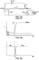
- Figs. 1A and 1B illustrate a conventional battery reversal protection circuit including a Schottky diode.
- Fig. 2A is a circuit diagram which illustrates schematically what happens during a load dump.
- Fig. 2B is a graph which illustrates the voltage across the load before and during a load dump in the circuit of Fig. 2A.
- Fig. 2C is a graph which illustrates the current through the generator and the protective zener diode before and during a load dump in the circuit of Fig. 2A.
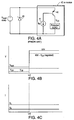
- Fig. 3A illustrates a conventional load dump protection circuit which includes a series resistor and a zener diode voltage clamp.
- Fig. 3B is a graph which illustrates the behavior of the voltage across the load before and during a load dump in the circuit of Fig. 3A.
- Fig. 3C is a graph which illustrates the current through the zener diode voltage clamp before and during a load dump in the circuit of Fig. 3A.
- Fig. 4A illustrates a circuit diagram of a conventional load dump protective circuit which includes a bipolar transistor.
- Fig. 4B is a graph which illustrates the voltage across the load before and during a load dump in the circuit of Fig. 4A.
- Fig. 4C is a graph which illustrates the current through the load before and during a load dump in the circuit of Fig. 4A.
- Fig. 5A illustrates a protective device in accordance with the invention in which the source of the depletion mode MOSFET is tied to the gate of the depletion mode MOSFET.
- Fig. 5B illustrates a protective device according to the invention in which the gate of the depletion mode MOSFET is tied to ground.
- Fig. 5C illustrates a protective device according to the invention in which the gate of the depletion mode MOSFET is tied to a reference voltage between the source voltage and ground.
- Fig. 5D illustrates a protective device in accordance with the invention in which the gate of the depletion mode MOSFET is connected to the cathode of a zener diode connected between ground and the source of the depletion mode MOSFET.
- Fig. 6A is a graph which illustrates the behavior of the current through the depletion mode MOSFET in the embodiments of Figs. 5A-5D as the voltage is increased, and compares this current with the currents in the circuits shown in Figs. 3A and 4A.
- Fig. 6B is a graph which illustrates the power consumed in the depletion mode MOSFET in the embodiments shown in Figs. 5A-5D as the voltage is increased, and compares this power with the power consumed in the circuits shown in Figs. 3A and 4A.
- Fig. 7A illustrates an alternative protective device in accordance with the invention in which the gate of the depletion mode MOSFET is switched from the source voltage to ground during a load dump condition.
- Fig. 7B illustrates an alternative protective device in accordance with the invention in which the gate of the depletion mode MOSFET is switched from the source voltage to a reference voltage during a load dump condition.
- Fig. 8A is a graph which compares the current through the MOSFET as a function of voltage in switched and unswitched embodiments of the invention.
- Fig. 8B is a graph which compares the power consumed in the MOSFET as a function of voltage in switched and unswitched embodiments of the invention.
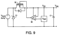
- Fig. 9 illustrates an alternative protective device in which the gate voltage of the depletion mode MOSFET is controlled by negative feedback.
- Figs. 10A-10C illustrate a protective device which also protects against a reversed input voltage.
- the embodiments according to this invention include a depletion mode MOSFET connected in series with the load that is to be protected.
- Fig. 5A illustrates the basic circuit which includes a MOSFET 50 that is connected in series with a load 51.
- a diode D1 connected between the drain of MOSFET 50 and ground has a relatively high breakdown voltage of, for example, 70 V.
- a second diode D2 connected between the source of MOSFET 50 and ground (in parallel with load 51) typically has a lower breakdown voltage which may be, for example, 8 V (for a 5 V circuit) or 18 V (for a 15 V circuit).
- Diodes D1 and D2 are not absolutely necessary to the circuit but they are beneficial in some ways. In integrated implementations, diodes D1 and D2 may be unavoidably present.
- Diode D1 may be associated with the drain-to-substrate junction of an integrated version of a DMOS transistor while-diode D2 may be present in a CMOS transistor pair or in an electrostatic discharge (ESD) protection structure. If present, diode D1 must have an avalanche breakdown value in excess of the load dump voltage to prevent unwanted conduction during the load dump transient. Conduction during load dump would most likely destroy diode D1.
- ESD electrostatic discharge
- the pinch-off voltage V p of depletion mode MOSFET 50 will fall somewhere in the range of -1 V to -4 V.
- diode D2 is not in breakdown and, assuming that V p and the device size of MOSFET 50 have been properly chosen, MOSFET 50 will behave as a resistor.
- MOSFET 50 will support the incremental voltage, saturate and begin to current limit.
- MOSFET 50 is in the current-limiting mode, additional power can be dissipated in MOSFET 50 only by increases in voltage.
- the power dissipated in a saturated MOSFET 50 is a linear function of the input voltage.
- the gate of MOSFET 50 is tied to ground.
- V p of MOSFET 50 may be, for example, -8 V to allow V DD to rise to 8 V.
- the circuit shown in Fig. 5B naturally limits the value of V DD to a value near the pinch-off voltage (i.e., - V p ), unless too much load current is demanded for the size of depletion mode MOSFET 50.
- the gate of MOSFET 50 may be tied to a reference voltage between ground and the source voltage of MOSFET 50, as shown in Fig. 5C, or to the cathode of a zener diode D3 as shown in Fig. 5D.
- the voltage V DD is effectively limited to a maximum which is equal to the sum of the breakdown voltage of zener diode D3 and the absolute value of the pinch-off voltage of MOSFET 50.
- MOSFET 50 operates in its linear region acting like a series resistor having a resistance R ds .
- MOSFET 50 current saturates, becoming a constant current source. The current through load 51 does not increase in proportion to the load dump voltage.
- Fig. 6A illustrates the behavior of current as a function of voltage for the resistive approach (Fig. 3A), the bipolar transistor approach (Fig. 4A) and the depletion MOSFET approach shown in Figs. 5A-5D.
- the current does not increase until after the battery voltage exceeds the breakdown voltage of diode D2, i.e., 20 V.
- MOSFET 50 and resistor 30 are selected to offer the same linear resistance, the current then rises linearly until MOSFET 50 saturates and limits the current.
- the current through resistor 30 continues to increase linearly.
- the PNP transistor 40 behaves somewhat like MOSFET 30 except that the presence of a base current increases the total current through the device.
- Fig. 6B illustrates power loss as a function of voltage for the same devices.
- the power losses in all three devices increase linearly until the breakdown of the zener diode, although the power losses in bipolar transistor 40 are somewhat greater.
- the power losses then begin to increase geometrically (by a square law).
- bipolar transistor 30 and MOSFET 50 current saturate the power losses again begin to increase linearly while the power losses through resistor 30 continue to increase geometrically.
- Figs. 7A and 7B illustrate improved embodiments in which the gate of MOSFET 50 is switched when a load dump occurs.
- the circuit of Fig. 7A includes a comparator 70 having a negative input terminal connected to a reference voltage V ref and a positive input connected to the anode of a zener diode D4.
- the output of comparator 70 is connected to an inverter 71 whose output is connected to the gate of MOSFET 50.
- V DD increases, breaking down zener diode D4 which forms a voltage divider with a resistor 72.
- the positive input of comparator 70 rises above V ref and comparator 70 outputs a voltage which causes inverter 71 to apply ground potential to the gate of MOSFET 50.
- I d (sat) k(V p - BV zener ) 2 where BV zener is the breakdown voltage of zener diode D4. If it is desired not to have zener diode D2 breakdown at a high battery voltage of 18 V, zener diode D4 could have a breakdown voltage of 15 V.
- the gate of MOSFET 50 may be switched to an intermediate bias during load dump, using the circuit shown in Fig. 7B.
- inverter 71 applies a predetermined reference voltage V REF to the gate of MOSFET 50 during a load dump.
- Figs. 8A and 8B show the current through and power dissipated by MOSFET 50 with increasing voltage when the gate is fixed (Figs. 5A-5D) and switched (Figs. 7A and 7B).
- the bump which is shown in the curves for the switched gate occurs because it takes time for the switching to occur.
- the voltage detection may be performed on the drain side of depletion mode MOSFET 50, although in this case the detection circuitry must be able to survive a load dump.
- a differential amplifier 90 applies a negative feedback voltage to the gate of MOSFET 50 so as to limit increases in V DD .
- the positive input of differential amplifier 90 is connected to a reference voltage V REF and the negative input of amplifier 90 is connected to V DD .
- a capacitor C1 provides filtering to prevent the circuit from oscillating.
- differential amplifier 90 applies a negative voltage to the gate of MOSFET 50, thereby reducing the current flow through MOSFET 50 and limiting increases in V DD . Since the gate drive for depletion mode MOSFET 50 does not exceed the voltage on the positive power supply rail, no charge pump is needed to drive this device.
- MOSFET 50 is normally on and is therefore capable of supplying start up current before the control circuitry driving its gate is activated during the initial application of power.
- the load dump protective circuitry of this invention may be combined with a device to protect the circuit elements against a reversed battery connection.
- a diode D5 has been added to the circuit, with its anode connected to V batt and its cathode connected to the drain of MOSFET 50.
- the basic load dump circuitry in Fig. 10A corresponds to the circuit shown in Fig. 5A
- the circuit shown in Fig. 10B corresponds to the circuit shown in Fig. 7B
- the circuit shown in Fig. 10C corresponds to the circuit shown in Fig. 9. Absent diode D5, a reversed battery condition could cause excessive current in diode D1.
Landscapes
- Engineering & Computer Science (AREA)
- Power Engineering (AREA)
- Protection Of Static Devices (AREA)
- Emergency Protection Circuit Devices (AREA)
- Semiconductor Integrated Circuits (AREA)
- Electronic Switches (AREA)
- Insulated Gate Type Field-Effect Transistor (AREA)
Applications Claiming Priority (2)
| Application Number | Priority Date | Filing Date | Title |
|---|---|---|---|
| US325860 | 1994-10-19 | ||
| US08/325,860 US5585991A (en) | 1994-10-19 | 1994-10-19 | Protective circuit for protecting load against excessive input voltage |
Publications (2)
| Publication Number | Publication Date |
|---|---|
| EP0708515A1 true EP0708515A1 (fr) | 1996-04-24 |
| EP0708515B1 EP0708515B1 (fr) | 2000-07-19 |
Family
ID=23269773
Family Applications (1)
| Application Number | Title | Priority Date | Filing Date |
|---|---|---|---|
| EP95116302A Expired - Lifetime EP0708515B1 (fr) | 1994-10-19 | 1995-10-16 | Circuit de protection pour la protection d'une charge contre une tension d'entrée trop élevée |
Country Status (4)
| Country | Link |
|---|---|
| US (1) | US5585991A (fr) |
| EP (1) | EP0708515B1 (fr) |
| JP (1) | JP4031539B2 (fr) |
| DE (1) | DE69518049T2 (fr) |
Cited By (11)
| Publication number | Priority date | Publication date | Assignee | Title |
|---|---|---|---|---|
| WO2005039935A1 (fr) * | 2003-09-24 | 2005-05-06 | Robert Bosch Gmbh | Circuiterie a protection contre l'inversion de polarite pour un vehicule automobile |
| EP1349255A3 (fr) * | 2002-03-25 | 2006-06-07 | Sila Holding Industriale S.p.A. | Circuit d'interface entre une source de tension à courant continu et un circuit pour entraîner une charge |
| EP2132850A4 (fr) * | 2007-04-05 | 2012-04-11 | Georgia Tech Res Inst | Protection contre les surtensions |
| US8488285B2 (en) | 2005-10-24 | 2013-07-16 | Georgia Tech Research Corporation | Active current surge limiters with watchdog circuit |
| GB2501326A (en) * | 2012-04-20 | 2013-10-23 | Continental Automotive Systems | Over-voltage protection system for a semiconductor device |
| US8582262B2 (en) | 2005-01-31 | 2013-11-12 | Georgia Tech Research Corporation | Active current surge limiters with disturbance sensor and multistage current limiting |
| FR3016751A1 (fr) * | 2014-01-21 | 2015-07-24 | Mersen France Sb Sas | Dispositif de protection d'un circuit contre des surtensions et organe d'alimentation electrique comprenant un tel dispositif |
| US9270170B2 (en) | 2011-04-18 | 2016-02-23 | Innovolt, Inc. | Voltage sag corrector using a variable duty cycle boost converter |
| US9299524B2 (en) | 2010-12-30 | 2016-03-29 | Innovolt, Inc. | Line cord with a ride-through functionality for momentary disturbances |
| US10205313B2 (en) | 2015-07-24 | 2019-02-12 | Symptote Technologies, LLC | Two-transistor devices for protecting circuits from sustained overcurrent |
| US10770883B2 (en) | 2015-09-21 | 2020-09-08 | Sympote Technologies LLC | One-transistor devices for protecting circuits and autocatalytic voltage conversion therefor |
Families Citing this family (33)
| Publication number | Priority date | Publication date | Assignee | Title |
|---|---|---|---|---|
| JP3368124B2 (ja) * | 1995-10-26 | 2003-01-20 | キヤノン株式会社 | 過充電防止回路 |
| US6185082B1 (en) | 1999-06-01 | 2001-02-06 | System General Corporation | Protection circuit for a boost power converter |
| DE19964097A1 (de) * | 1999-12-31 | 2001-07-26 | Nokia Mobile Phones Ltd | Schutzschaltung für eine elektronische Einheit gegen länger anhaltende Überspannung |
| JP2002299569A (ja) * | 2001-03-29 | 2002-10-11 | Sanyo Electric Co Ltd | スイッチング用mosトランジスタの保護回路 |
| DE10135168A1 (de) * | 2001-07-19 | 2003-02-13 | Bosch Gmbh Robert | Vorrichtung zum Schutz elektronischer Bauelemente |
| US6700765B2 (en) * | 2002-05-31 | 2004-03-02 | Delphi Technologies, Inc. | High current series-pass over-voltage protection circuit |
| AU2003259268A1 (en) * | 2002-07-29 | 2004-02-16 | Raytheon Company | Method and system for protecting a vehicle system from a load dump |
| US6882513B2 (en) * | 2002-09-13 | 2005-04-19 | Ami Semiconductor, Inc. | Integrated overvoltage and reverse voltage protection circuit |
| US6970337B2 (en) * | 2003-06-24 | 2005-11-29 | Linear X Systems Inc. | High-voltage low-distortion input protection current limiter |
| JP4574960B2 (ja) * | 2003-06-24 | 2010-11-04 | ルネサスエレクトロニクス株式会社 | 車両用電源制御装置及び制御チップ |
| JP4148162B2 (ja) * | 2004-03-05 | 2008-09-10 | 株式会社デンソー | 回路システム |
| US7271989B2 (en) * | 2004-06-03 | 2007-09-18 | Altera Corporation | Electrostatic discharge protection circuit |
| US7139157B2 (en) * | 2004-07-30 | 2006-11-21 | Kyocera Wireless Corp. | System and method for protecting a load from a voltage source |
| US7245135B2 (en) * | 2005-08-01 | 2007-07-17 | Touchdown Technologies, Inc. | Post and tip design for a probe contact |
| JP2007329998A (ja) * | 2006-06-06 | 2007-12-20 | Ricoh Co Ltd | 過電圧保護回路、過電圧保護回路の過電圧保護方法及び過電圧保護回路を有する半導体装置 |
| CN101291108B (zh) * | 2007-04-19 | 2010-11-17 | 立锜科技股份有限公司 | 电荷泵启动电路与方法 |
| US7489182B2 (en) * | 2007-05-17 | 2009-02-10 | Richtek Technology Corporation | Charge pump start up circuit and method thereof |
| US7800869B1 (en) | 2007-08-27 | 2010-09-21 | National Semiconductor Corporation | Apparatus and method for power supply overvoltage disconnect protection |
| US7660090B1 (en) | 2007-08-27 | 2010-02-09 | National Semiconductor Corporation | Apparatus and method for input voltage transient protection with a low-voltage reset circuit |
| US7561394B2 (en) * | 2007-12-10 | 2009-07-14 | Visteon Global Technologies, Inc. | System and method for overvoltage protection |
| US8922961B2 (en) * | 2009-09-25 | 2014-12-30 | Hamilton Sundstrand Corporation | Two-level lightning protection circuit |
| DE102009046606A1 (de) * | 2009-11-11 | 2011-05-12 | Robert Bosch Gmbh | Schutzelement für elektronische Schaltungen |
| JP5558938B2 (ja) * | 2010-06-30 | 2014-07-23 | 日立アロカメディカル株式会社 | 超音波診断装置の受信入力保護回路 |
| CN102315629A (zh) * | 2010-07-01 | 2012-01-11 | 鸿富锦精密工业(深圳)有限公司 | 保护电路及具有该保护电路的电子装置 |
| JP5593904B2 (ja) * | 2010-07-16 | 2014-09-24 | 株式会社リコー | 電圧クランプ回路およびこれを用いた集積回路 |
| US8659860B2 (en) * | 2011-07-14 | 2014-02-25 | Cooper Technologies Company | Transient voltage blocking for power converter |
| JP2013074749A (ja) * | 2011-09-28 | 2013-04-22 | Seiko Instruments Inc | 過充電防止回路及び半導体装置 |
| US20130295869A1 (en) * | 2012-05-01 | 2013-11-07 | Microsemi Corporation | Square law extension technique for high speed radio detection |
| FR2994750B1 (fr) | 2012-08-23 | 2015-12-11 | St Microelectronics Rousset | Alimentation d'une charge a potentiel flottant |
| US10516262B2 (en) * | 2016-12-01 | 2019-12-24 | Osypka Medical Gmbh | Overvoltage protection device and method |
| US11095111B2 (en) * | 2018-04-02 | 2021-08-17 | Allegro Microsystems, Llc | Systems and methods for transient pulse protection |
| JP2024109320A (ja) * | 2023-02-01 | 2024-08-14 | 株式会社東芝 | 集積回路装置 |
| DE102024107357A1 (de) * | 2024-03-14 | 2025-09-18 | Bayerische Motoren Werke Aktiengesellschaft | Entgegenwirken einer kritischen Belastung in einem Energiebordnetz |
Citations (3)
| Publication number | Priority date | Publication date | Assignee | Title |
|---|---|---|---|---|
| EP0305935A2 (fr) * | 1987-08-31 | 1989-03-08 | National Semiconductor Corporation | Circuit de protection contre une chute de charge de VDD |
| EP0401410A1 (fr) * | 1989-06-08 | 1990-12-12 | Siemens Aktiengesellschaft | Circuit de protection de circuits électroniques contre les surtensions |
| US6737393B2 (en) | 2001-04-10 | 2004-05-18 | Mon-Sheng Lin | Liquid bubble solution for producing luminous bubbles |
Family Cites Families (2)
| Publication number | Priority date | Publication date | Assignee | Title |
|---|---|---|---|---|
| US5302889A (en) * | 1992-06-19 | 1994-04-12 | Honeywell Inc. | Voltage regulator |
| US5517379A (en) * | 1993-05-26 | 1996-05-14 | Siliconix Incorporated | Reverse battery protection device containing power MOSFET |
-
1994
- 1994-10-19 US US08/325,860 patent/US5585991A/en not_active Expired - Lifetime
-
1995
- 1995-10-13 JP JP29219795A patent/JP4031539B2/ja not_active Expired - Lifetime
- 1995-10-16 DE DE69518049T patent/DE69518049T2/de not_active Expired - Lifetime
- 1995-10-16 EP EP95116302A patent/EP0708515B1/fr not_active Expired - Lifetime
Patent Citations (3)
| Publication number | Priority date | Publication date | Assignee | Title |
|---|---|---|---|---|
| EP0305935A2 (fr) * | 1987-08-31 | 1989-03-08 | National Semiconductor Corporation | Circuit de protection contre une chute de charge de VDD |
| EP0401410A1 (fr) * | 1989-06-08 | 1990-12-12 | Siemens Aktiengesellschaft | Circuit de protection de circuits électroniques contre les surtensions |
| US6737393B2 (en) | 2001-04-10 | 2004-05-18 | Mon-Sheng Lin | Liquid bubble solution for producing luminous bubbles |
Non-Patent Citations (1)
| Title |
|---|
| "ANNOUNCEMENT", RADIO FERNSEHEN ELEKTRONIK, vol. 42, no. 2, 1 February 1993 (1993-02-01), pages 61, XP000407295 * |
Cited By (29)
| Publication number | Priority date | Publication date | Assignee | Title |
|---|---|---|---|---|
| EP1349255A3 (fr) * | 2002-03-25 | 2006-06-07 | Sila Holding Industriale S.p.A. | Circuit d'interface entre une source de tension à courant continu et un circuit pour entraîner une charge |
| US7282809B2 (en) | 2002-03-25 | 2007-10-16 | Sila Holdings Industriale S.P.A. | Interface circuit between a direct-current voltage source and a circuit for driving a load, particularly for use in motor-vehicles |
| WO2005039935A1 (fr) * | 2003-09-24 | 2005-05-06 | Robert Bosch Gmbh | Circuiterie a protection contre l'inversion de polarite pour un vehicule automobile |
| US8582262B2 (en) | 2005-01-31 | 2013-11-12 | Georgia Tech Research Corporation | Active current surge limiters with disturbance sensor and multistage current limiting |
| US8766481B2 (en) | 2005-01-31 | 2014-07-01 | Georgia Tech Research Corporation | Reduction of inrush current due to voltage sags with switch and shunt resistance |
| US8643989B2 (en) | 2005-01-31 | 2014-02-04 | Georgia Tech Research Corporation | Active current surge limiters with inrush current anticipation |
| US8587913B2 (en) | 2005-01-31 | 2013-11-19 | Georgia Tech Research Corporation | Active current surge limiters with voltage detector and relay |
| US9065266B2 (en) | 2005-10-24 | 2015-06-23 | Georgia Tech Research Corporation | Reduction of inrush current due to voltage sags by an isolating current limiter |
| US9048654B2 (en) | 2005-10-24 | 2015-06-02 | Georgia Tech Research Corporation | Reduction of inrush current due to voltage sags by impedance removal timing |
| US8488285B2 (en) | 2005-10-24 | 2013-07-16 | Georgia Tech Research Corporation | Active current surge limiters with watchdog circuit |
| US8411403B2 (en) | 2007-04-05 | 2013-04-02 | Georgia Tech Research Corporation | Voltage surge and overvoltage protection with current surge protection |
| US8593776B2 (en) | 2007-04-05 | 2013-11-26 | Georgia Tech Research Corporation | Voltage surge and overvoltage protection using prestored voltage-time profiles |
| US8335067B2 (en) | 2007-04-05 | 2012-12-18 | Georgia Tech Research Corporation | Voltage surge and overvoltage protection with sequenced component switching |
| US8335068B2 (en) | 2007-04-05 | 2012-12-18 | Georgia Tech Research Corporation | Voltage surge and overvoltage protection using prestored voltage-time profiles |
| US8325455B2 (en) | 2007-04-05 | 2012-12-04 | Georgia Tech Research Corporation | Voltage surge and overvoltage protection with RC snubber current limiter |
| EP2132850A4 (fr) * | 2007-04-05 | 2012-04-11 | Georgia Tech Res Inst | Protection contre les surtensions |
| US9071048B2 (en) | 2007-04-05 | 2015-06-30 | Georgia Tech Research Corporation | Voltage surge and overvoltage protection by distributed clamping device dissipation |
| US9299524B2 (en) | 2010-12-30 | 2016-03-29 | Innovolt, Inc. | Line cord with a ride-through functionality for momentary disturbances |
| US9270170B2 (en) | 2011-04-18 | 2016-02-23 | Innovolt, Inc. | Voltage sag corrector using a variable duty cycle boost converter |
| US9030792B2 (en) | 2012-04-20 | 2015-05-12 | Continental Automotive Systems, Inc. | Overvoltage protection method using exposed device supply rail |
| GB2501326A (en) * | 2012-04-20 | 2013-10-23 | Continental Automotive Systems | Over-voltage protection system for a semiconductor device |
| FR3016751A1 (fr) * | 2014-01-21 | 2015-07-24 | Mersen France Sb Sas | Dispositif de protection d'un circuit contre des surtensions et organe d'alimentation electrique comprenant un tel dispositif |
| EP2911257A1 (fr) * | 2014-01-21 | 2015-08-26 | MERSEN France SB SAS | Dispositif de protection d'un circuit contre des surtensions et alimentation électrique comprenant un tel dispositif |
| US10205313B2 (en) | 2015-07-24 | 2019-02-12 | Symptote Technologies, LLC | Two-transistor devices for protecting circuits from sustained overcurrent |
| US11031769B2 (en) | 2015-07-24 | 2021-06-08 | Symptote Technologies, LLC | Two-transistor devices for protecting circuits from sustained overcurrent |
| US10770883B2 (en) | 2015-09-21 | 2020-09-08 | Sympote Technologies LLC | One-transistor devices for protecting circuits and autocatalytic voltage conversion therefor |
| US11355916B2 (en) | 2015-09-21 | 2022-06-07 | Symptote Technologies Llc | One-transistor devices for protecting circuits and autocatalytic voltage conversion therefor |
| US11611206B2 (en) | 2015-09-21 | 2023-03-21 | Symptote Technologies Llc | One-transistor devices for protecting circuits and autocatalytic voltage conversion therefor |
| US11962141B2 (en) | 2015-09-21 | 2024-04-16 | Symptote Technologies Llc | One-transistor devices for protecting circuits and autocatalytic voltage conversion therefor |
Also Published As
| Publication number | Publication date |
|---|---|
| US5585991A (en) | 1996-12-17 |
| JPH08213619A (ja) | 1996-08-20 |
| JP4031539B2 (ja) | 2008-01-09 |
| DE69518049D1 (de) | 2000-08-24 |
| HK1014402A1 (en) | 1999-09-24 |
| EP0708515B1 (fr) | 2000-07-19 |
| DE69518049T2 (de) | 2000-12-21 |
Similar Documents
| Publication | Publication Date | Title |
|---|---|---|
| EP0708515B1 (fr) | Circuit de protection pour la protection d'une charge contre une tension d'entrée trop élevée | |
| KR102838077B1 (ko) | 보호 버스에서 접지로 연결된 fet 디바이스를 갖는 보호 회로 | |
| US6717785B2 (en) | Semiconductor switching element driving circuit | |
| US7724046B2 (en) | High side/low side driver device for switching electrical loads | |
| US4679112A (en) | Transistor protection circuit for automotive motor control applications | |
| US5781390A (en) | Integrated supply protection | |
| US6169439B1 (en) | Current limited power MOSFET device with improved safe operating area | |
| KR102066367B1 (ko) | 보호 회로 및 보호 회로의 동작 방법, 및 반도체 집적 회로 장치 | |
| US5343053A (en) | SCR electrostatic discharge protection for integrated circuits | |
| EP0736974A1 (fr) | Circuit d'attaque pour une grille | |
| US5789951A (en) | Monolithic clamping circuit and method of preventing transistor avalanche breakdown | |
| US4808839A (en) | Power field effect transistor driver circuit for protection from overvoltages | |
| US7288856B2 (en) | Reverse battery protection circuit for power switch | |
| GB2322745A (en) | Emitter resistance for improving IGBT short-circuit capability | |
| EP1137068B1 (fr) | Dispositif semi-conducteur de puissance ayant un circuit de protection | |
| US7327546B2 (en) | Power switching circuit with active clamp disconnect for load dump protection | |
| US6700765B2 (en) | High current series-pass over-voltage protection circuit | |
| CN109285726B (zh) | 具有温度保护的用于对电感器进行放电的放电电路 | |
| KR960036012A (ko) | 정전 방전으로부터 보호하기 위한 구조물을 가진 반도체 소자 | |
| US4665459A (en) | Method and circuit for dissipating stored inductive energy | |
| US6819535B2 (en) | Device for protecting loads supplied by an alternator | |
| EP0375037A2 (fr) | Protection de circuit intégré de puissance contre les surtensions de charge | |
| US5731729A (en) | Voltage transient suppression circuit for preventing overvoltages in power transistor systems | |
| HK1014402B (en) | Protective circuit for protecting load against excessive input voltage | |
| EP4718697A1 (fr) | Circuit d'alimentation et procédé de commande applicable à celui-ci |
Legal Events
| Date | Code | Title | Description |
|---|---|---|---|
| PUAI | Public reference made under article 153(3) epc to a published international application that has entered the european phase |
Free format text: ORIGINAL CODE: 0009012 |
|
| AK | Designated contracting states |
Kind code of ref document: A1 Designated state(s): DE FR GB IT NL |
|
| 17P | Request for examination filed |
Effective date: 19960904 |
|
| 17Q | First examination report despatched |
Effective date: 19970604 |
|
| GRAG | Despatch of communication of intention to grant |
Free format text: ORIGINAL CODE: EPIDOS AGRA |
|
| GRAG | Despatch of communication of intention to grant |
Free format text: ORIGINAL CODE: EPIDOS AGRA |
|
| GRAH | Despatch of communication of intention to grant a patent |
Free format text: ORIGINAL CODE: EPIDOS IGRA |
|
| GRAH | Despatch of communication of intention to grant a patent |
Free format text: ORIGINAL CODE: EPIDOS IGRA |
|
| GRAA | (expected) grant |
Free format text: ORIGINAL CODE: 0009210 |
|
| AK | Designated contracting states |
Kind code of ref document: B1 Designated state(s): DE FR GB IT NL |
|
| REF | Corresponds to: |
Ref document number: 69518049 Country of ref document: DE Date of ref document: 20000824 |
|
| ET | Fr: translation filed | ||
| ITF | It: translation for a ep patent filed | ||
| PLBE | No opposition filed within time limit |
Free format text: ORIGINAL CODE: 0009261 |
|
| STAA | Information on the status of an ep patent application or granted ep patent |
Free format text: STATUS: NO OPPOSITION FILED WITHIN TIME LIMIT |
|
| 26N | No opposition filed | ||
| REG | Reference to a national code |
Ref country code: GB Ref legal event code: IF02 |
|
| PGFP | Annual fee paid to national office [announced via postgrant information from national office to epo] |
Ref country code: NL Payment date: 20031002 Year of fee payment: 9 |
|
| PGFP | Annual fee paid to national office [announced via postgrant information from national office to epo] |
Ref country code: FR Payment date: 20041020 Year of fee payment: 10 |
|
| PG25 | Lapsed in a contracting state [announced via postgrant information from national office to epo] |
Ref country code: NL Free format text: LAPSE BECAUSE OF NON-PAYMENT OF DUE FEES Effective date: 20050501 |
|
| NLV4 | Nl: lapsed or anulled due to non-payment of the annual fee |
Effective date: 20050501 |
|
| PG25 | Lapsed in a contracting state [announced via postgrant information from national office to epo] |
Ref country code: FR Free format text: LAPSE BECAUSE OF NON-PAYMENT OF DUE FEES Effective date: 20060630 |
|
| REG | Reference to a national code |
Ref country code: FR Ref legal event code: ST Effective date: 20060630 |
|
| PGFP | Annual fee paid to national office [announced via postgrant information from national office to epo] |
Ref country code: DE Payment date: 20141029 Year of fee payment: 20 Ref country code: GB Payment date: 20141027 Year of fee payment: 20 |
|
| PGFP | Annual fee paid to national office [announced via postgrant information from national office to epo] |
Ref country code: IT Payment date: 20141027 Year of fee payment: 20 |
|
| REG | Reference to a national code |
Ref country code: DE Ref legal event code: R071 Ref document number: 69518049 Country of ref document: DE |
|
| REG | Reference to a national code |
Ref country code: GB Ref legal event code: PE20 Expiry date: 20151015 |
|
| PG25 | Lapsed in a contracting state [announced via postgrant information from national office to epo] |
Ref country code: GB Free format text: LAPSE BECAUSE OF EXPIRATION OF PROTECTION Effective date: 20151015 |