EP0708525B1 - Ein Rechtecksignal liefernde Leistungsverstärkerstufe mit gesteuerter Amplitude - Google Patents
Ein Rechtecksignal liefernde Leistungsverstärkerstufe mit gesteuerter Amplitude Download PDFInfo
- Publication number
- EP0708525B1 EP0708525B1 EP95202722A EP95202722A EP0708525B1 EP 0708525 B1 EP0708525 B1 EP 0708525B1 EP 95202722 A EP95202722 A EP 95202722A EP 95202722 A EP95202722 A EP 95202722A EP 0708525 B1 EP0708525 B1 EP 0708525B1
- Authority
- EP
- European Patent Office
- Prior art keywords
- transistors
- current
- pair
- amplifier stage
- voltage
- Prior art date
- Legal status (The legal status is an assumption and is not a legal conclusion. Google has not performed a legal analysis and makes no representation as to the accuracy of the status listed.)
- Expired - Lifetime
Links
- 230000001105 regulatory effect Effects 0.000 title description 2
- 238000006243 chemical reaction Methods 0.000 claims description 3
- 230000007423 decrease Effects 0.000 description 5
- 238000010586 diagram Methods 0.000 description 4
- 238000004519 manufacturing process Methods 0.000 description 4
- 230000001052 transient effect Effects 0.000 description 4
- 230000001276 controlling effect Effects 0.000 description 3
- 230000000694 effects Effects 0.000 description 2
- 230000010287 polarization Effects 0.000 description 2
- 230000005236 sound signal Effects 0.000 description 2
- 230000004075 alteration Effects 0.000 description 1
- 230000005540 biological transmission Effects 0.000 description 1
- 230000005669 field effect Effects 0.000 description 1
- 230000001939 inductive effect Effects 0.000 description 1
- 238000000034 method Methods 0.000 description 1
- 230000003071 parasitic effect Effects 0.000 description 1
- 230000008569 process Effects 0.000 description 1
- 230000009467 reduction Effects 0.000 description 1
- 230000035945 sensitivity Effects 0.000 description 1
- 230000007704 transition Effects 0.000 description 1
Images
Classifications
-
- H—ELECTRICITY
- H03—ELECTRONIC CIRCUITRY
- H03F—AMPLIFIERS
- H03F3/00—Amplifiers with only discharge tubes or only semiconductor devices as amplifying elements
- H03F3/20—Power amplifiers, e.g. Class B amplifiers, Class C amplifiers
- H03F3/21—Power amplifiers, e.g. Class B amplifiers, Class C amplifiers with semiconductor devices only
- H03F3/217—Class D power amplifiers; Switching amplifiers
- H03F3/2173—Class D power amplifiers; Switching amplifiers of the bridge type
-
- H—ELECTRICITY
- H03—ELECTRONIC CIRCUITRY
- H03F—AMPLIFIERS
- H03F3/00—Amplifiers with only discharge tubes or only semiconductor devices as amplifying elements
- H03F3/30—Single-ended push-pull [SEPP] amplifiers; Phase-splitters therefor
- H03F3/3081—Duplicated single-ended push-pull arrangements, i.e. bridge circuits
Definitions
- the present invention as defined in the claims relates to an amplifier stage power delivering a rectangular signal on a load by means an amplifier of the so-called "bridge" type with two pairs of transistors bipolar of the same type of conductivity, a first pair of transistors whose transmitters are respectively connected to load terminals as well as the collectors of the transistors of the second pair of transistors, a plurality of switching devices alternately applying a voltage of amplitude control on the respective bases of the transistors of the first pair and synchronizing the basic polarization transistors of the second pair.
- a power stage of this kind is known from the document EP-A-0 587 945.
- a rectangular type signal is created at the terminals of a load by means of eight switches including four are actuated in phase and four actuated in reverse phase.
- the amplitude of the signal obtained on the load is regulated by making call for switching a capacity that is, by means of two switches, alternately connected to the terminals of the load then connected to the input of a feedback amplifier for comparison with a reference voltage.
- GB-A-2 070 371 also discloses an example of a "bridge" output stage.
- the known amplifier stage has been designed to supply a load whose impedance is resistive and possibly inductive and to avoid instability related to the feedback of the amplifier and the parasitic capacities of the circuit. He is bad suitable for controlling a load whose impedance would be mainly capacitive as is the case with a piezoelectric transducer sound signal generator. Because such a charge is not not crossed by a direct current, the voltage signal which would obtained using the known amplifier stage would be very distorted with a noticeable loss of signal harmonics. Creation high harmonics is on the contrary sought to increase the acoustic efficiency of this kind of transducer, in particular in the case of warning signals, for example in a device telephone.
- the amplifier stage known from the cited document is reveals to be relatively complicated especially with regard to the number high of switches used to create the pulse signal rectangular on the load.
- the object of the invention is to provide an amplifier stage of power of simple structure and therefore integrable in a way economical, which is suitable for controlling a dominant load capacitive such as a piezoelectric transducer.
- Another purpose of the invention is to provide a power amplifier stage capable of constitute a ringing function among other functions performed by an integrated circuit intended for application to receivers telephone, ringtone whose sound level could be adjusted to willingness by the user, including at a low level, without alteration of the ring tone.
- the invention is based in particular on the idea that a signal rectangular switching will be correctly applied on a load capacitive if the voltages applied to the ends of the load are generated under a sufficiently low direct current impedance.
- the power amplifier stage of the type stated in the introductory paragraph is characterized according to the present invention, in that the bases of the four amplifier transistors are connected respectively to four current sources delivering substantially equal currents and in that the transistors of the second pair are alternately connected in diodes by means of two of the switch devices.
- the invention requires only four switch devices for controlling the bridge amplifier, instead of eight switches used in the amplifier stage of the prior art, for the sole control of the bridge amplifier.
- the amplifier stage according to the invention avoids the use of a feedback as well as the instability problems associated therewith when the load used is predominantly capacitive. However, this amplifier stage allows rapid switching of the voltage of the output signal and ensures precise control of the amplitude of this signal, even at a low level, of the order of 1/10 th of peak volt.
- the operating characteristics of the amplifier stage of power according to the invention can be made practically independent of the fluctuations in the gain of the transistors (variations due to the manufacturing process) as well as variations in temperature in an embodiment of the invention characterized in what the current sources supplying the bases are realized at by means of a current mirror comprising four outputs paired between them and an input powered by the basic current of a fifth transistor, of the same type of conductivity as that of the first four transistors, which transistor has its emitter powered by a source reference current.
- the four basic currents generated are compared to the base current of the fifth transistor which has its emitter current fixed by a reference source stable.
- the emitter currents of the four transistors forming the bridge amplifier are therefore made substantially identical to the current of the fifth transistor, or even a multiple of this current depending on whether the current mirror has a current ratio of output on input current equal to or greater than the unit.
- the invention advantageously provides that the voltage of amplitude control comes from a voltage generator comprising digital-to-analog converter for signal conversion control numerals applied at the input of this generator.
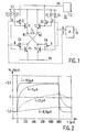
- Figure 1 shows the electrical diagram of an amplifier stage power according to the invention.
- Figure 2 shows the appearance of the output signals from the Figure 1 for several values of continuous polarization of transistors.
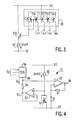
- Figure 3 shows the preferred embodiment of a basic current generator, with four outputs, for use in the amplifier stage according to the invention.
- Figure 4 shows the diagram of a voltage generator amplitude control adapted to the control of the amplifier stage Figure 1.
- a power amplifier stage conforming to the invention includes an amplifier of the "in bridge "provided with two pairs of bipolar NPN transistors, one first pair of transistors T1, T2 whose emitters are respectively connected to the ends of a load L as well as to collectors of a second pair of transistors T3, T4 whose transmitters are connected to a supply terminal V1 used to voltage reference.
- the collectors of the two transistors of the first pair T1, T2 are connected to a supply voltage positive V2.
- a voltage generator 12 supplies a voltage of VA control which is adjustable and applied to the bases of transistors T1 and T2, alternatively, by means of two devices switches S1, S2.
- the transistors T3 and T4 of the second pair of transistors are connected in diodes alternately by means of two switch devices S3, S4.
- the switch devices S1 to S4 are controlled by a switching signal generator 13 which determines the frequency and the duty cycle of the signals rectangular to be supplied on the load L. It is arranged so the switch devices S1 and S3 are closed simultaneously while the switch devices S2 and S4 are actuated in phase opposition.
- the switching devices can be constituted by MOS type field effect transistors.
- the four transistors T1-T4 of the bridge amplifier have each their base connected respectively to four current sources 31-34, these current sources essentially supplying a current identical, from the supply voltage V2. This provision is particularly well suited for actuating a load L whose the impedance is essentially capacitive as is the case with a piezoelectric transducer.
- the generator 13 provides a determining signal A the opening of switch devices S2 and S4 and provides a signal B which is the inverse of signal A determining the closure of switch devices S1 and S3.
- Control voltage amplitude VA is applied to the base of transistor T1 which acts as a transmitter-follower and supplies a terminal N1 with charge L, this voltage, reduced by a transmitter-base voltage drop.
- the transistor T4 whose collector is connected to the same terminal N1 of the load L absorbs a current equal to ⁇ times the current supplied by the base current source 34, ( ⁇ being the value of the current gain transistors).
- V BE emitter-base voltage drop
- the transistor T3, connected in diode constitutes an impedance weak for the transmission of transient currents from the terminal N2 from load L to supply line V1, while a maximum limit of this impedance is set by the emitter current of transistor T2, current which is equal to ( ⁇ + 1) times the current of current source 33 supplying the base of this transistor.
- the emitter-base voltage of the transistor of the first pair operating as an emitter follower decreases over time since the current passing through the load L decreases itself.
- the voltage drop decreases over time since the current flowing through this diode decreases.
- the limit values of these two V BEs are set by the direct current supplied by the transistors under the effect of the basic current sources 31 to 34. The time for establishing the amplitude steps of the rectangular signal to be generated on the load L can therefore be set to the desired value by choosing the direct current value supplied by the transistors.
- FIG. 2 represents the shape of the output signals of the amplifier stage of FIG. 1, for different values of direct current passing through the transistors T1 to T4, over time t .
- Load L has a capacity of 80nF.
- the voltage Vs at the terminals of the load L is observed for a peak voltage of 0.1 Volt.
- the parameter I indicated is the value of the direct current applied to the transistors T1-T4, that is to say ⁇ times the current of the current sources 31-34.
- FIG. 3 shows the diagram of a basic current generator particularly suitable for producing current sources 31 to 34 of FIG. 1.
- This generator includes a current mirror 20 composed of five PNP type transistors, one input transistor T30 and four output transistors T31 to T34.
- the transistors T31 to T34 are paired with each other so the currents delivered by their respective collector 41 to 44 are equal currents between them.
- a other condition to obtain reproducible performance in function of possible variations in the manufacturing process and in function of variations in operating temperature is to supply the input transistor T30 of the current mirror 20 with the base current of an NPN T20 transistor whose emitter is supplied by a reference current Iref1 supplied by a current source of reference 40.
- the reference current Iref1 can be made independent of temperature by means well known to specialists.
- the current drawn by the transistors T1 to T4 of the bridge amplifier will nevertheless be subject to equal to the current supplied by transistor T20.
- the currents charged by the transistors T31 and T34 will be proportional to the base current of current T20 and the emitter / collector currents of transistors T1 to T4 will themselves be proportional to the current of reference Iref1.
- the generator of amplitude control voltages to supply a voltage VA whose value comprises a fixed part equal to 2.V BE and a part which varies according to the law of variation which is desired.
- the load L is a piezoelectric transducer for the production of a sound signal, it is desirable that the progression of this variable part of the control voltage be faster than a linear variation, so as to approach the sensitivity of the human ear and for example, that the variable part varies according to a geometric progression.
- FIG. 4 shows the diagram of an example of generator of amplitude control voltage.
- the generator 12 includes a source of reference current 50 flowing from the voltage positive supply V2 a reference current Iref2 in a transistor 51 connected as a diode and whose emitter is connected to the reference supply voltage V1.
- the voltage drop of the diode 51 under the effect of the current Iref2 is applied to the input of a amplifier 52 of unit gain whose output 53 has the same voltage than the input voltage but under a low impedance.
- the generator 12 further comprises a digital-analog converter 56 for converting digital input signals Cd in an analog current Ia supplying a resistor 54 by a end 58 the other end being connected to the output 53 of amplifier 52.
- the converter 56 can be arranged to provide eight current values Ia staged between 1 ⁇ A and 128 ⁇ A, the values are succeeding each other by a factor of 2.
- the end 58 of the resistor 54 therefore has a voltage which on the one hand is proportional to the current Ia representing the variable part of the voltage control plus a fixed voltage drop in the diode 51.
- This end 58 is connected to the input of another amplifier 60 whose voltage gain is set to 2 by means of a against reaction of two equal resistors denoted R in FIG. 3.
- This amplifier 60 outputs the voltage VA which will be used to control the amplitude of the signal delivered by the amplifier in bridge.
- the control signal VA therefore has a fixed part corresponding to twice the voltage drop in transistor 51 and it thus makes it possible to obtain on the load L an amplitude equal to the variable part of the VA control signal.
- V BE A precise compensation of V BE is obtained when the Iref2 current of the current source reference 50 is in proper relationship with the Iref1 current from the current source 40 shown in Figure 3 taking into account the area ratios of the transistors involved , both in the current mirror 20 (FIG. 3) and in the bridge amplifier shown in FIG. 1.
Landscapes
- Engineering & Computer Science (AREA)
- Power Engineering (AREA)
- Amplifiers (AREA)
Claims (3)
- Eine Leistungsverstärkerstufe, die ein Rechtecksignal auf eine mittlere Ladung eines "Brücken"-Verstärkertyps mit zwei bipolaren Transistorpaaren gleicher Leitfähigkeit abgibt, einen ersten Teil des Transistors, dessen Emitter jeweils an die Ladeklemmen sowie jeweils an die Kollektoren der Transistoren des zweiten Transistorpaars angeschlossen sind, eine Vielzahl an Unterbrechervorrichtungen, die abwechselnd eine Amplitudensteuerspannung auf die jeweiligen Basen der Transistoren des ersten Teils anwenden und synchron die Basispolarisierung der Transistoren des zweiten Teils ändern,
dadurch gekennzeichnet, daß die Basen der vier Transistoren des Verstärkers jeweils mit vier Stromquellen verbunden sind, die grundlegend gleiche Ströme abgeben, und daß die Transistoren des zweiten Paars dagegen unter Verwendung von zwei Unterbrechervorrichtungen als Dioden geschaltet sind. - Leistungsverstärkerstufe nach Anspruch 1, dadurch gekennzeichnet, daß diese die Basen versorgenden Stromquellen mit einem Stromspiegel mit vier untereinander gepaarten Ausgängen und einem Eingang hergestellt werden, der vom Basisstrom eines fünften Transistors versorgt wird und derselben Leitfähigkeit wie die der ersten und zweiten Paare ist, wobei der Emitter dieses Transistors von einer Referenzstromquelle versorgt wird.
- Leistungsverstärkerstufe nach Anspruch 2, dadurch gekennzeichnet, daß die Amplitudensteuerspannung aus einem Spannungsgenerator herrührt, der einen Digital-Analog-Wandler für die Umwandlung der dem Eingang dieses Generators zugeführten digitalen Steuersignale aufweist.
Applications Claiming Priority (2)
| Application Number | Priority Date | Filing Date | Title |
|---|---|---|---|
| FR9412489 | 1994-10-19 | ||
| FR9412489A FR2726138A1 (fr) | 1994-10-19 | 1994-10-19 | Etage amplificateur de puissance delivrant un signal rectangulaire d'amplitude controlee |
Publications (2)
| Publication Number | Publication Date |
|---|---|
| EP0708525A1 EP0708525A1 (de) | 1996-04-24 |
| EP0708525B1 true EP0708525B1 (de) | 1998-01-21 |
Family
ID=9468007
Family Applications (1)
| Application Number | Title | Priority Date | Filing Date |
|---|---|---|---|
| EP95202722A Expired - Lifetime EP0708525B1 (de) | 1994-10-19 | 1995-10-10 | Ein Rechtecksignal liefernde Leistungsverstärkerstufe mit gesteuerter Amplitude |
Country Status (5)
| Country | Link |
|---|---|
| US (1) | US5631605A (de) |
| EP (1) | EP0708525B1 (de) |
| JP (1) | JP3562885B2 (de) |
| DE (1) | DE69501492T2 (de) |
| FR (1) | FR2726138A1 (de) |
Families Citing this family (7)
| Publication number | Priority date | Publication date | Assignee | Title |
|---|---|---|---|---|
| EP0906661A2 (de) * | 1997-04-07 | 1999-04-07 | Koninklijke Philips Electronics N.V. | Treiberverstärker in brückenschaltung und telekommunikationsgerät |
| US5990739A (en) * | 1998-01-22 | 1999-11-23 | Lam; Peter Ar-Fu | Analog signal amplifier |
| DE19837439C2 (de) * | 1998-08-18 | 2000-07-13 | Siemens Ag | Verfahren und Vorrichtung zum Erzeugen von Ansteuersignalen für eine Leistungsendstufe und Leistungsendstufe |
| GB9911505D0 (en) * | 1999-05-19 | 1999-07-14 | New Transducers Ltd | Transducer driver |
| IT1318881B1 (it) * | 2000-09-19 | 2003-09-10 | St Microelectronics Srl | Circuito di pilotaggio ad alta efficienza per carichi capacitivi. |
| RU2263943C2 (ru) * | 2002-01-08 | 2005-11-10 | Федеральное государственное унитарное предприятие "Производственное объединение "Уральский оптико-механический завод" (ФГУП "ПО "УОМЗ") | Кибернетическая микропроцессорная цифровая система |
| US10153795B1 (en) * | 2018-02-20 | 2018-12-11 | Nxp B.V. | Switching amplifier circuit with amplitude control |
Family Cites Families (8)
| Publication number | Priority date | Publication date | Assignee | Title |
|---|---|---|---|---|
| SU581568A1 (ru) * | 1975-10-21 | 1977-11-25 | Ленинградский Ордена Ленина Электротехнический Институт Им.В.И.Ульянова (Ленина) | Мостовой усилитель мощности |
| JPS5694994A (en) * | 1979-12-28 | 1981-07-31 | Matsushita Electric Ind Co Ltd | Output circuit |
| US4638260A (en) * | 1984-09-21 | 1987-01-20 | Hamley James P | Audio amplifier |
| JPH03240013A (ja) * | 1990-02-19 | 1991-10-25 | Nikon Corp | コンパクトな広角ズームレンズ |
| ES2090788T3 (es) * | 1992-07-07 | 1996-10-16 | Siemens Ag | Circuito excitador integrable para una carga reactiva. |
| EP0587945A1 (de) * | 1992-09-18 | 1994-03-23 | Mietec Alcatel | Schaltung zur Amplitudenregelung |
| US5382915A (en) * | 1993-07-06 | 1995-01-17 | Motorola, Inc. | Pulsewidth-modulated amplifier having analog mode |
| FR2712126B1 (fr) * | 1993-11-05 | 1995-12-01 | Thomson Csf | Amplificateur de puissance du type pont en H et ses moyens de blocage et dispositif amplificateur de puissance comportant de tels amplificateurs. |
-
1994
- 1994-10-19 FR FR9412489A patent/FR2726138A1/fr not_active Withdrawn
-
1995
- 1995-10-10 EP EP95202722A patent/EP0708525B1/de not_active Expired - Lifetime
- 1995-10-10 DE DE69501492T patent/DE69501492T2/de not_active Expired - Lifetime
- 1995-10-16 JP JP26721695A patent/JP3562885B2/ja not_active Expired - Lifetime
- 1995-10-18 US US08/544,504 patent/US5631605A/en not_active Expired - Lifetime
Also Published As
| Publication number | Publication date |
|---|---|
| US5631605A (en) | 1997-05-20 |
| EP0708525A1 (de) | 1996-04-24 |
| JPH08204465A (ja) | 1996-08-09 |
| FR2726138A1 (fr) | 1996-04-26 |
| DE69501492D1 (de) | 1998-02-26 |
| JP3562885B2 (ja) | 2004-09-08 |
| DE69501492T2 (de) | 1998-07-23 |
Similar Documents
| Publication | Publication Date | Title |
|---|---|---|
| FR2702317A1 (fr) | Circuit pompe de charge à faible consommation, faible bruit et synthétiseur de fréquence équipé d'un tel circuit. | |
| EP0511707B1 (de) | Kaskodendifferenzverstärker | |
| EP0487386B1 (de) | Frequenzvervielfacher | |
| EP0660512A1 (de) | Phasenschiebverstärker und seine Verwendung in einer Zusammenführungsschaltung | |
| FR2485295A1 (fr) | Circuit de commande d'impedance par reaction | |
| EP0836271A1 (de) | Integrierter Oszillator und einen solchen Oszillator verwendendes Funktelefon | |
| EP0194177B1 (de) | Teilnehmerschnittstellenschaltung mit Überwachungsbetrieb bei verringerter Speisung | |
| EP0708525A1 (de) | Ein Rechtecksignal liefernde Leistungsverstärkerstufe mit gesteuerter Amplitude | |
| EP0649079A1 (de) | Geregelter Spannungsquellengenerator der Bandgapbauart | |
| EP0230693B1 (de) | Hochfrequenz-Differenzverstärkerstufe und Verstärker mit einer solchen Differenzverstärkerstufe | |
| EP0021509B1 (de) | Elektronischer Teilnehmerverbindungssatz | |
| FR2664445A1 (fr) | Circuit amplificateur differentiel a faible distorsion et procede d'utilisation. | |
| EP1925079B1 (de) | Stromschalter mit durch eine niederspannung gespeisten differenztransistorpaaren | |
| FR2813481A1 (fr) | Modulateur de frequence a faible bruit ayant une frequence porteuse variable | |
| EP1081848A1 (de) | Frequenzumsetzer mit unterdrücktem Lecksignal aus einem lokalen Oszillator und Verfahren | |
| FR2730363A1 (fr) | Amplificateur a gain eleve en hautes frequences et oscillateur a circuit resonant muni d'un tel amplificateur | |
| FR2466137A1 (fr) | Convertisseur de signaux | |
| FR2477802A1 (fr) | Circuit d'amplification | |
| FR2471100A1 (fr) | Circuit d'alimentation de ligne telephonique | |
| EP0716503B1 (de) | Verstärker mit reduzierter Verzerrung | |
| FR2755804A1 (fr) | Mise en veille d'un regulateur lineaire | |
| FR2578666A1 (fr) | Circuit de commande a compensation des variations de la tension anodique, pour etage de deviation verticale de televiseur | |
| FR2486733A1 (fr) | Circuit amplificateur | |
| FR2462058A1 (fr) | Amplificateur ayant une zone morte de largeur et position reglables | |
| FR2482382A1 (fr) | Circuit a miroir de courant a haute impedance de sortie et a basse " perte de tension " |
Legal Events
| Date | Code | Title | Description |
|---|---|---|---|
| PUAI | Public reference made under article 153(3) epc to a published international application that has entered the european phase |
Free format text: ORIGINAL CODE: 0009012 |
|
| AK | Designated contracting states |
Kind code of ref document: A1 Designated state(s): DE FR GB IT |
|
| 17P | Request for examination filed |
Effective date: 19961024 |
|
| GRAG | Despatch of communication of intention to grant |
Free format text: ORIGINAL CODE: EPIDOS AGRA |
|
| 17Q | First examination report despatched |
Effective date: 19970120 |
|
| GRAH | Despatch of communication of intention to grant a patent |
Free format text: ORIGINAL CODE: EPIDOS IGRA |
|
| GRAH | Despatch of communication of intention to grant a patent |
Free format text: ORIGINAL CODE: EPIDOS IGRA |
|
| RAP1 | Party data changed (applicant data changed or rights of an application transferred) |
Owner name: PHILIPS ELECTRONICS N.V. Owner name: PHILIPS COMPOSANTS ET SEMICONDUCTEURS |
|
| GRAA | (expected) grant |
Free format text: ORIGINAL CODE: 0009210 |
|
| AK | Designated contracting states |
Kind code of ref document: B1 Designated state(s): DE FR GB IT |
|
| REF | Corresponds to: |
Ref document number: 69501492 Country of ref document: DE Date of ref document: 19980226 |
|
| ITF | It: translation for a ep patent filed | ||
| GBT | Gb: translation of ep patent filed (gb section 77(6)(a)/1977) |
Effective date: 19980325 |
|
| PLBE | No opposition filed within time limit |
Free format text: ORIGINAL CODE: 0009261 |
|
| STAA | Information on the status of an ep patent application or granted ep patent |
Free format text: STATUS: NO OPPOSITION FILED WITHIN TIME LIMIT |
|
| 26N | No opposition filed | ||
| REG | Reference to a national code |
Ref country code: FR Ref legal event code: TP |
|
| REG | Reference to a national code |
Ref country code: GB Ref legal event code: IF02 |
|
| REG | Reference to a national code |
Ref country code: GB Ref legal event code: 746 Effective date: 20020911 |
|
| REG | Reference to a national code |
Ref country code: FR Ref legal event code: D6 |
|
| REG | Reference to a national code |
Ref country code: GB Ref legal event code: 732E |
|
| REG | Reference to a national code |
Ref country code: GB Ref legal event code: 732E |
|
| REG | Reference to a national code |
Ref country code: FR Ref legal event code: TP |
|
| REG | Reference to a national code |
Ref country code: FR Ref legal event code: GC |
|
| REG | Reference to a national code |
Ref country code: FR Ref legal event code: RG |
|
| REG | Reference to a national code |
Ref country code: FR Ref legal event code: ST Effective date: 20090630 |
|
| PG25 | Lapsed in a contracting state [announced via postgrant information from national office to epo] |
Ref country code: FR Free format text: LAPSE BECAUSE OF NON-PAYMENT OF DUE FEES Effective date: 20081031 |
|
| REG | Reference to a national code |
Ref country code: FR Ref legal event code: D3 |
|
| PGRI | Patent reinstated in contracting state [announced from national office to epo] |
Ref country code: FR Effective date: 20101103 |
|
| PGFP | Annual fee paid to national office [announced via postgrant information from national office to epo] |
Ref country code: DE Payment date: 20100930 Year of fee payment: 16 |
|
| PGFP | Annual fee paid to national office [announced via postgrant information from national office to epo] |
Ref country code: GB Payment date: 20110926 Year of fee payment: 17 |
|
| PGFP | Annual fee paid to national office [announced via postgrant information from national office to epo] |
Ref country code: IT Payment date: 20110924 Year of fee payment: 17 |
|
| PGFP | Annual fee paid to national office [announced via postgrant information from national office to epo] |
Ref country code: FR Payment date: 20111118 Year of fee payment: 17 |
|
| GBPC | Gb: european patent ceased through non-payment of renewal fee |
Effective date: 20121010 |
|
| REG | Reference to a national code |
Ref country code: FR Ref legal event code: ST Effective date: 20130628 |
|
| PG25 | Lapsed in a contracting state [announced via postgrant information from national office to epo] |
Ref country code: DE Free format text: LAPSE BECAUSE OF NON-PAYMENT OF DUE FEES Effective date: 20130501 Ref country code: GB Free format text: LAPSE BECAUSE OF NON-PAYMENT OF DUE FEES Effective date: 20121010 |
|
| REG | Reference to a national code |
Ref country code: DE Ref legal event code: R119 Ref document number: 69501492 Country of ref document: DE Effective date: 20130501 |
|
| PG25 | Lapsed in a contracting state [announced via postgrant information from national office to epo] |
Ref country code: IT Free format text: LAPSE BECAUSE OF NON-PAYMENT OF DUE FEES Effective date: 20121010 Ref country code: FR Free format text: LAPSE BECAUSE OF NON-PAYMENT OF DUE FEES Effective date: 20121031 |