EP0708986B1 - Pyrodetektorelement mit orientiert aufgewachsener pyroelektrischer schicht und verfahren zu seiner herstellung - Google Patents
Pyrodetektorelement mit orientiert aufgewachsener pyroelektrischer schicht und verfahren zu seiner herstellung Download PDFInfo
- Publication number
- EP0708986B1 EP0708986B1 EP94920390A EP94920390A EP0708986B1 EP 0708986 B1 EP0708986 B1 EP 0708986B1 EP 94920390 A EP94920390 A EP 94920390A EP 94920390 A EP94920390 A EP 94920390A EP 0708986 B1 EP0708986 B1 EP 0708986B1
- Authority
- EP
- European Patent Office
- Prior art keywords
- layer
- pyrodetector
- silicon substrate
- pyroelectric
- oriented
- Prior art date
- Legal status (The legal status is an assumption and is not a legal conclusion. Google has not performed a legal analysis and makes no representation as to the accuracy of the status listed.)
- Expired - Lifetime
Links
Images
Classifications
-
- H—ELECTRICITY
- H10—SEMICONDUCTOR DEVICES; ELECTRIC SOLID-STATE DEVICES NOT OTHERWISE PROVIDED FOR
- H10N—ELECTRIC SOLID-STATE DEVICES NOT OTHERWISE PROVIDED FOR
- H10N15/00—Thermoelectric devices without a junction of dissimilar materials; Thermomagnetic devices, e.g. using the Nernst-Ettingshausen effect
- H10N15/10—Thermoelectric devices using thermal change of the dielectric constant, e.g. working above and below the Curie point
-
- G—PHYSICS
- G01—MEASURING; TESTING
- G01J—MEASUREMENT OF INTENSITY, VELOCITY, SPECTRAL CONTENT, POLARISATION, PHASE OR PULSE CHARACTERISTICS OF INFRARED, VISIBLE OR ULTRAVIOLET LIGHT; COLORIMETRY; RADIATION PYROMETRY
- G01J5/00—Radiation pyrometry, e.g. infrared or optical thermometry
- G01J5/10—Radiation pyrometry, e.g. infrared or optical thermometry using electric radiation detectors
- G01J5/34—Radiation pyrometry, e.g. infrared or optical thermometry using electric radiation detectors using capacitors, e.g. pyroelectric capacitors
Definitions
- a pyrodetector consists of an active sensor layer a pyroelectric material, which is covered on both sides with a Electrode is coated.
- a pyroelectric material for example, lead zirconate titanate (PZT) is preferred Lead titanate or organic pyroelectrics such as polyvinylidene fluoride (PVDF) used. Permanent polarization of the pyroelectric can be done in a strong electrical field or arises with oriented growth of the pyroelectric by itself.
- detector elements are included "floating" polysilicon membranes at a distance of about 1 ⁇ m known to the substrate surface. Even the etching of thin ones Silicon membranes and free-standing tongues made of silicon as well etching wells in the silicon substrate under the pyroelectric Layer is known. To selectively oppose the substrate pyroelectric layer or against the first electrode layer to etch, an additional one is set up before the detector element is set up Etching stop layer built up on the substrate, for example an amorphous layer made of silicon dioxide or silicon nitride is.
- the polarization direction of the pyroelectric should be perpendicular to the electrode surfaces and thus perpendicular to the substrate surface. Since the polarization of the perovskites from the PZT family can only take certain directions in the crystal, the pyroelectric layer must at least be oriented and, even better, applied epitaxially to the substrate. Certain single-crystalline substrate materials are required for this. From R. Takayama, Y. Tomita, J. Asayama, K. Nomura and H.
- From US-A-3 816 750 is a hot-pressed one more ceramic pyrodetector based on Lathan-doped Lead circonate titanate known.
- the problem underlying the present invention is a Specify thin-film pyrodetector element, which consists of an oriented pyroelectric thin film is built, a has low heat capacity and that a simpler and more integrated electrical connection for construction and operation of the Detector arrays enabled.
- the membrane or the buffer layer can be of any thickness generated, but usually has such a thickness that they are together with the active part of the pyrodetector element has sufficient mechanical stability to the through Etch back the substrate now "substrate-free" space under the active Bridge detector area without a break or one other damage during the operation of the pyrodetector element to fear.
- One embodiment of the invention relates to the use of a spinel layer (MgAl 2 O 4 ) as an intermediate layer, over which a magnesium oxide layer grows epitaxially or at least in an oriented manner.
- the first electrode layer is then applied to the magnesium oxide surface.
- Platinum, which grows oriented to epitaxially above the magnesium oxide, is particularly suitable for the first electrode layer.
- a perovskite from the PZT family is selected for the pyroelectric layer to be applied thereon, for example a lead titanate PbTiO 3 , which shows an oriented growth over magnesium oxide or over the platinum electrode layer in between.
- the material for the second or upper electrode layer over The pyroelectric layer is not critical as it is one sufficient conductivity only with the pyroelectric Material, especially with the lead compatibility contained therein must have and incoming heat radiation as possible should absorb well.
- a nickel / chrome alloy for the second electrode layer it is possible a nickel / chrome alloy for the second electrode layer to use.
- a fully stabilized yttrium-stabilized zirconium oxide ZrO 2 (YSZ) is used as the buffer layer, which was previously known only as a buffer layer for high-temperature superconductors.
- platinum can be used as the first electrode layer, since it grows on YSZ.
- the pyroelectric layer is then again formed by a lead titanate, for example by (Pb, Ca) (Ti, Mn) O 3 .
- the first electrode layer above the YSZ buffer layer is produced from an electronically conductive ABO 3 material, for which manganates and cobaltates are particularly suitable.
- a lead titanate layer for example (Pb, Ca) (Ti, Mn) O 3 , is then applied as a pyroelectric layer over a first electrode layer made of, for example, (La, Ca) MnO 3 .
- the material combination electrode / pyroelectric is chosen so that both layers contain the same cations and differ only in the cation ratio on the A and B sites.
- a material combination according to the invention therefore consists in a first electrode layer of (La, Pb) Mn, Ti) O 3 and (Pb, La) (Ti, Mn) O 3 as a pyroelectric layer.
- This embodiment results in a particularly simple manufacture, the electrode and pyroelectric material being able to represent two different layers, or together forming a single layer with a corresponding gradient of the cation ratio. A particularly good lattice match and subsequently a particularly highly oriented pyroelectric layer can be generated.
- Pyrodetector elements are known thin-film methods suitable, for example sputtering, MOCVD, sol-money spin-on, Pulsed laser deposition or other gas phase and plasma deposition processes.
- the degree of orientation of the growing up Can be grown up by a correspondingly slow growth and suitably chosen wax-up temperatures can be increased.
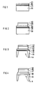
- Figure 1 On a monocrystalline silicon substrate SS with (100) oriented and polished surface, a sequence of layers is applied over the entire surface using known thin-film methods, for example by sputtering, vapor deposition CVD, MOCVD etc. An intermediate layer ZS made of spinel MgAl 2 O 4 is applied directly over the silicon substrate SS, a buffer layer BS made of magnesium oxide MgO over it and the first electrode layer E1 over it.
- the different layers are optionally applied with different deposition conditions with regard to temperature, pressure or process, the deposition temperature and the growth rate achieved allowing the growth of at least oriented, better epitaxial layers.
- intermediate layer ZS, buffer layer BS and first electrode layer E1 are chosen to be as thin as possible in order to achieve the best possible orientation when growing up despite the lattice mismatch.
- Intermediate layer ZS and buffer layer BS should, however, be so thick and mechanically stable that they fulfill their membrane function and can at least freely carry the pyrodetector element or pyrodetector array built up over its surface.
- a layer thickness of approx. 1 ⁇ m is sufficient for this.
- the minimum thickness of the first electrode layer E1 is limited by the current conductivity of the material of the first electrode layer.
- a metallic and, for example, platinum first electrode layer can be made correspondingly thinner at approximately 100 nm than, for example, an electrode layer made of an electrically conductive ABO 3 compound.
- a pyroelectric is now over the first electrode layer E1 Layer PS of a lead titanate with a thickness of approx. 1 ⁇ m grew up oriented.
- the second electrode layer E2 is over the entire surface over the pyroelectric Layer PS applied, for example by Evaporating a metal and then using a photo-structuring technique structured, i.e. by application a photoresist, imagewise exposing a desired one Structure, development of the photoresist and removal of the electrode layer E2 in areas not covered by photoresist, for example by etching.
- a photostructuring technique structured, i.e. by application a photoresist, imagewise exposing a desired one Structure, development of the photoresist and removal of the electrode layer E2 in areas not covered by photoresist, for example by etching.
- a further photostructuring step becomes the uniform pyroelectric layer PS in a variety of individual detectors Layer areas divided, for example by etching.
- the spatial separation of individual detectors in a pyrodetector array is necessary to move between two adjacent single detectors a thermal bridge and thus the crosstalk when detecting to minimize an IR signal.
- the first electrode layer E1 again with photostructuring processes be structured.
- Figure 2 shows this arrangement.
- the lower electrode can also be left over the entire surface.
- an absorber layer is finally applied, for example consists of gold black.
- Substrate of the pyrodetector element is now the substrate SS in Area of the pyrodetector (s) etched away. It is possible using a photoresist technique under each individual detector to produce a recess in the substrate SS, or in larger ones Recesses a number of individual detectors at the same time to expose, or the substrate under this row of individual detectors to remove.
- This is used for the alkaline etching of the silicon substrate SS Intermediate layer ZS as an etch stop layer.
- the one on the top of the silicon substrate applied layer structure of the pyrodetector elements is in this etching step by a suitable Protected cover layer.
- Figure 3 shows the arrangement after this step.
- the intermediate layer ZS is exposed in the recess A of the silicon substrate SS in the region of the pyrodetector element (E1, PS, E2).
- the recess can correspond exactly to the dimensions of the pyrodetector element, or can be made somewhat larger or smaller.
- a suitable base area for an individual pyrodetector element is, for example, 50 ⁇ 50 ⁇ m 2 , a pyrodetector array comprising at least two times two, that is to say four individual detectors. A better spatial resolution of a detected IR signal is obtained with larger arrays, which consist of more individual detectors.
- the circuits used to operate a pyrodetector element or a pyrodetector array are preferred integrated on the silicon substrate SS. They consist in essentially from readout circuit for addressing the individual detectors and amplifier circuits for amplifying the weak Measurement signals. The circuits are normally generated before producing the pyrodetector element or the pyrodetector elements.
- Figure 4 shows a further embodiment of the invention, at that of the first electrode layer E1, pyroelectric Layer PS and second electrode layer E2 existing pyrodetector element on a buffer layer BS made of yttrium stabilized zirconium oxide (YSZ).
- YSZ yttrium stabilized zirconium oxide
- the compact design allows for a lower primary signal to work from the pyrodetector element because the signal is in immediate Proximity to the detector element through suitable circuits can be reinforced.
- the structure of the pyrodetector element as a thin layer also enables faster response of the pyrodetector against incident IR radiation.
Landscapes
- Engineering & Computer Science (AREA)
- Power Engineering (AREA)
- Physics & Mathematics (AREA)
- General Physics & Mathematics (AREA)
- Spectroscopy & Molecular Physics (AREA)
- Photometry And Measurement Of Optical Pulse Characteristics (AREA)
- Radiation Pyrometers (AREA)
Description
- die Figuren 1 bis 3
- einen schematischen Querschnitt durch ein erfindungsgemäßes Pyrodetektorelement während verschiedener Verfahrensstufen bei der Herstellung und
- Figur 4
- einen schematischen Querschnitt durch ein fertiges Pyrodetektorelement nach einer weiteren Ausführungsform der Erfindung.
Claims (11)
- Pyrodetektorelement in Dünnschichtbauweise mitodera) einem monokristallinen Siliziumsubstrat (SS)b) einer über dem Siliziumsubstrat aufgebrachten, epitaktischen Bufferschicht (BS) aus Yttrium-stabilisiertem Zirkonoxid YSZ
einer über dem Siliziumsubstrat aufgebrachten epitaktischen Zwischenschicht (ZS) aus Spinell und einer darüber aufgebrachten zumindest orientierten Bufferschicht (BS) aus Magnesiumoxidc) einer orientierten oder epitaktischen ersten Elektrodenschicht (E1)d) einer c-Achsen-orientierten pyroelektrischen Schicht (PS) aus der Familie der Perowskite unde) einer zweiten Elektrodenschicht (E2). - Pyrodetektorelement nach Anspruch 1,
bei dem die erste Elektrodenschicht (E1) aus Platin besteht. - Pyrodetektorelement nach Anspruch 1,
bei dem die erste Elektrodenschicht (E1) aus einem elektrisch leitenden Oxid aus der Klasse der Perowskite mit der allgemeinen Summenformel (LaCa) (MnCo) O3 oder (LaPbCa) (MnCoTi) O3 besteht und bei dem die pyroelektrische Schicht (PS) aus den gleichen Komponenten wie die erste Elektrodenschicht (E1) besteht, jedoch ein anderes Kationenverhaltnis aufweist. - Pyrodetektorelement nach Anspruch 3,
bei dem die erste Elektrodenschicht (E1) und die pyroelektrische Schicht (PS) zumindest einen gemeinsamen Bereich mit einem sich kontinuierlich in Richtung Schichtdicke ändernden Kationenverhaltnis aufweisen. - Pyrodetektorelement nach Anspruch 1 oder 2,
bei dem die pyroelektrische Schicht ein Perowskitmaterial aus der Familie der Bleizirkonattitanate umfaßt. - Pyrodetektorelement nach einem der vorangehenden Ansprüche,
bei dem das Siliziumsubstrat (SS) im Bereich der aktiven Sensorfläche des Pyrodetektorelements eine die Zwischenschicht (ZS) oder die Bufferschicht (BS) freilegende Ausnehmung (A) besitzt. - Pyrodetektorelement nach einem der vorangehenden Ansprüche,
welches Teil einer Anordnung von mehreren Pyrodetektorelementen auf einem gemeinsamen Siliziumsubstrat (SS) ist. - Verfahren zur Herstellung eines Pyrodetektorelements in Dünnschichtbauweise mit den SchrittenVorsehen eines monokristallinen Siliziumsubstrats (SS)orientiertes Aufwachsen einer Zwischenschicht (ZS) aus Spinellorientiertes Abscheiden einer Bufferschicht (BS) aus Magnesiumoxidorientiertes Abscheiden einer ersten Elektrodenschicht (E1)orientiertes Aufwachsen einer pyroelektrischen Schicht (PS) aus einem pyroelektrischen Material aus der Familie der PerowskiteErzeugen einer metallischen zweiten Elektrodenschicht (E2)Rückätzen des Siliziumsubstrats (SS) unter dem Pyrodetektorelement im Bereich dessen aktiver Sensorflache, wobei die Bufferschicht (BS) als Ätzstopschicht dient undHerstellung von elektrischen Anschlüssen zur elektrischen Verschaltung der beiden Elektrodenschichten.
- Verfahren zur Herstellung eines Pyrodetektorelements in Dünnschichtbauweise mit den SchrittenVorsehen eines monokristallinen Siliziumsubstrats (SS)orientiertes Abscheiden einer Bufferschicht (BS) aus Yttrium-stabilisiertem Zirkonoxid (YSZ)orientiertes Abscheiden einer ersten Elektrodenschicht (E1)orientiertes Aufwachsen einer pyroelektrischen Schicht (PS) aus einem pyroelektrischen Material aus der Familie der PerowskiteErzeugen einer metallischen zweiten Elektrodenschicht (E2)Rückätzen des Siliziumsubstrats (SS) unter dem Pyrodetektorelement im Bereich dessen aktiver Sensorfläche, wobei die Bufferschicht (BS) als Ätzstopschicht dient undHerstellung von elektrischen Anschlüssen zur elektrischen Verschaltung der beiden Elektrodenschichten.
- Verfahren nach Anspruch 8 oder 9,
bei dem nach ganzflächigem Aufbringen der einzelnen Schichten (E1, PS und E2) zumindest eine Photostrukturierungstechnik durchgeführt wird, um eine Anordnung mehrerer voneinander getrennter und daher thermisch gegeneinander isolierter Pyrodetektorelemente auf dem Siliziumsubstrat (SS) zu erzeugen. - Verfahren nach Anspruch 10,
bei dem im Siliziumsubstrat (SS) mikroelektronische Auslese- und Verstärkerschaltungen für die Anordnung der Pyrodetektorelemente auf dem Siliziumsubstrat vorgesehen werden.
Applications Claiming Priority (3)
| Application Number | Priority Date | Filing Date | Title |
|---|---|---|---|
| DE4323821 | 1993-07-15 | ||
| DE4323821A DE4323821A1 (de) | 1993-07-15 | 1993-07-15 | Pyrodetektorelement mit orientiert aufgewachsener pyroelektrischer Schicht und Verfahren zu seiner Herstellung |
| PCT/DE1994/000785 WO1995002904A1 (de) | 1993-07-15 | 1994-07-08 | Pyrodetektorelement mit orientiert aufgewachsener pyroelektrischer schicht und verfahren zu seiner herstellung |
Publications (2)
| Publication Number | Publication Date |
|---|---|
| EP0708986A1 EP0708986A1 (de) | 1996-05-01 |
| EP0708986B1 true EP0708986B1 (de) | 1998-04-01 |
Family
ID=6492938
Family Applications (1)
| Application Number | Title | Priority Date | Filing Date |
|---|---|---|---|
| EP94920390A Expired - Lifetime EP0708986B1 (de) | 1993-07-15 | 1994-07-08 | Pyrodetektorelement mit orientiert aufgewachsener pyroelektrischer schicht und verfahren zu seiner herstellung |
Country Status (5)
| Country | Link |
|---|---|
| US (1) | US5684302A (de) |
| EP (1) | EP0708986B1 (de) |
| JP (1) | JPH09500234A (de) |
| DE (2) | DE4323821A1 (de) |
| WO (1) | WO1995002904A1 (de) |
Cited By (1)
| Publication number | Priority date | Publication date | Assignee | Title |
|---|---|---|---|---|
| DE102004002914A1 (de) * | 2004-01-20 | 2005-08-11 | Siemens Ag | Vorrichtung und Verfahren zur Detektion mindestens einer Substanz |
Families Citing this family (43)
| Publication number | Priority date | Publication date | Assignee | Title |
|---|---|---|---|---|
| DE19601712C1 (de) * | 1996-01-18 | 1997-04-30 | Siemens Ag | Pyrodetektorelement |
| DE19605668C1 (de) * | 1996-02-15 | 1997-03-27 | Siemens Ag | Ferroelektrisches Bauelement und Verfahren zur Herstellung |
| US5945673A (en) * | 1996-08-30 | 1999-08-31 | Raytheon Company | Thermal detector with nucleation element and method |
| US5990481A (en) * | 1996-08-30 | 1999-11-23 | Raytheon Company | Thermal detector with preferentially-ordered thermally sensitive element and method |
| US6137107A (en) * | 1996-08-30 | 2000-10-24 | Raytheon Company | Thermal detector with inter-digitated thin film electrodes and method |
| US6020216A (en) * | 1996-08-30 | 2000-02-01 | Texas Instruments Incorporated | Thermal detector with stress-aligned thermally sensitive element and method |
| DE69737283T2 (de) * | 1996-09-27 | 2007-11-15 | Rohm Co. Ltd., Kyoto | Ferroelektrisches material, verfahren zu seiner herstellung, halbleiterspeicheranordnung und verfahren zu seiner herstellung |
| US5949071A (en) * | 1997-08-14 | 1999-09-07 | Sandia Corporation | Uncooled thin film pyroelectric IR detector with aerogel thermal isolation |
| US6087661A (en) * | 1997-10-29 | 2000-07-11 | Raytheon Company | Thermal isolation of monolithic thermal detector |
| RU2148802C1 (ru) * | 1999-01-27 | 2000-05-10 | Институт физики полупроводников СО РАН | Устройство регистрации теплового излучения |
| US6392257B1 (en) | 2000-02-10 | 2002-05-21 | Motorola Inc. | Semiconductor structure, semiconductor device, communicating device, integrated circuit, and process for fabricating the same |
| US6693033B2 (en) * | 2000-02-10 | 2004-02-17 | Motorola, Inc. | Method of removing an amorphous oxide from a monocrystalline surface |
| JP3514207B2 (ja) * | 2000-03-15 | 2004-03-31 | 株式会社村田製作所 | 強誘電体薄膜素子ならびにセンサ、および強誘電体薄膜素子の製造方法 |
| KR20030011083A (ko) | 2000-05-31 | 2003-02-06 | 모토로라 인코포레이티드 | 반도체 디바이스 및 이를 제조하기 위한 방법 |
| JP4612932B2 (ja) * | 2000-06-01 | 2011-01-12 | ホーチキ株式会社 | 赤外線検出素子および赤外線2次元イメージセンサ |
| WO2002009187A2 (en) | 2000-07-24 | 2002-01-31 | Motorola, Inc. | Heterojunction tunneling diodes and process for fabricating same |
| US6563118B2 (en) * | 2000-12-08 | 2003-05-13 | Motorola, Inc. | Pyroelectric device on a monocrystalline semiconductor substrate and process for fabricating same |
| US20020096683A1 (en) | 2001-01-19 | 2002-07-25 | Motorola, Inc. | Structure and method for fabricating GaN devices utilizing the formation of a compliant substrate |
| JP3732098B2 (ja) * | 2001-02-19 | 2006-01-05 | 株式会社ルネサステクノロジ | 半導体装置 |
| WO2002082551A1 (en) | 2001-04-02 | 2002-10-17 | Motorola, Inc. | A semiconductor structure exhibiting reduced leakage current |
| US7358578B2 (en) * | 2001-05-22 | 2008-04-15 | Renesas Technology Corporation | Field effect transistor on a substrate with (111) orientation having zirconium oxide gate insulation and cobalt or nickel silicide wiring |
| RU2210099C2 (ru) * | 2001-06-13 | 2003-08-10 | Омский государственный технический университет | Устройство термостатирования фотоприемника |
| US6709989B2 (en) | 2001-06-21 | 2004-03-23 | Motorola, Inc. | Method for fabricating a semiconductor structure including a metal oxide interface with silicon |
| US6992321B2 (en) | 2001-07-13 | 2006-01-31 | Motorola, Inc. | Structure and method for fabricating semiconductor structures and devices utilizing piezoelectric materials |
| US7019332B2 (en) | 2001-07-20 | 2006-03-28 | Freescale Semiconductor, Inc. | Fabrication of a wavelength locker within a semiconductor structure |
| US6693298B2 (en) | 2001-07-20 | 2004-02-17 | Motorola, Inc. | Structure and method for fabricating epitaxial semiconductor on insulator (SOI) structures and devices utilizing the formation of a compliant substrate for materials used to form same |
| US20030015768A1 (en) * | 2001-07-23 | 2003-01-23 | Motorola, Inc. | Structure and method for microelectromechanical system (MEMS) devices integrated with other semiconductor structures |
| US6855992B2 (en) | 2001-07-24 | 2005-02-15 | Motorola Inc. | Structure and method for fabricating configurable transistor devices utilizing the formation of a compliant substrate for materials used to form the same |
| US20030026310A1 (en) * | 2001-08-06 | 2003-02-06 | Motorola, Inc. | Structure and method for fabrication for a lighting device |
| US6639249B2 (en) * | 2001-08-06 | 2003-10-28 | Motorola, Inc. | Structure and method for fabrication for a solid-state lighting device |
| US20030034491A1 (en) | 2001-08-14 | 2003-02-20 | Motorola, Inc. | Structure and method for fabricating semiconductor structures and devices for detecting an object |
| US6673667B2 (en) * | 2001-08-15 | 2004-01-06 | Motorola, Inc. | Method for manufacturing a substantially integral monolithic apparatus including a plurality of semiconductor materials |
| US20030071327A1 (en) | 2001-10-17 | 2003-04-17 | Motorola, Inc. | Method and apparatus utilizing monocrystalline insulator |
| US6916717B2 (en) | 2002-05-03 | 2005-07-12 | Motorola, Inc. | Method for growing a monocrystalline oxide layer and for fabricating a semiconductor device on a monocrystalline substrate |
| US7169619B2 (en) | 2002-11-19 | 2007-01-30 | Freescale Semiconductor, Inc. | Method for fabricating semiconductor structures on vicinal substrates using a low temperature, low pressure, alkaline earth metal-rich process |
| US6885065B2 (en) | 2002-11-20 | 2005-04-26 | Freescale Semiconductor, Inc. | Ferromagnetic semiconductor structure and method for forming the same |
| US6806202B2 (en) | 2002-12-03 | 2004-10-19 | Motorola, Inc. | Method of removing silicon oxide from a surface of a substrate |
| US6963090B2 (en) | 2003-01-09 | 2005-11-08 | Freescale Semiconductor, Inc. | Enhancement mode metal-oxide-semiconductor field effect transistor |
| US7020374B2 (en) | 2003-02-03 | 2006-03-28 | Freescale Semiconductor, Inc. | Optical waveguide structure and method for fabricating the same |
| US6965128B2 (en) | 2003-02-03 | 2005-11-15 | Freescale Semiconductor, Inc. | Structure and method for fabricating semiconductor microresonator devices |
| US7750173B2 (en) * | 2007-01-18 | 2010-07-06 | Advanced Technology Materials, Inc. | Tantalum amido-complexes with chelate ligands useful for CVD and ALD of TaN and Ta205 thin films |
| JP5989296B2 (ja) * | 2010-04-28 | 2016-09-07 | ソニー株式会社 | 赤外線撮像装置 |
| CN104465850B (zh) * | 2014-11-28 | 2016-09-21 | 电子科技大学 | 基于石墨烯吸收层的热释电红外探测器及其制造方法 |
Family Cites Families (6)
| Publication number | Priority date | Publication date | Assignee | Title |
|---|---|---|---|---|
| US3816750A (en) * | 1971-06-04 | 1974-06-11 | Honeywell Inc | Pyroelectric detector |
| US4009516A (en) * | 1976-03-29 | 1977-03-01 | Honeywell Inc. | Pyroelectric detector fabrication |
| GB8812954D0 (en) * | 1988-06-01 | 1988-10-05 | Emi Plc Thorn | Thermal imaging |
| CA2118597C (en) * | 1991-11-04 | 2001-12-11 | Paul W. Kruse, Jr. | Thin film pyroelectric imaging array |
| US5270298A (en) * | 1992-03-05 | 1993-12-14 | Bell Communications Research, Inc. | Cubic metal oxide thin film epitaxially grown on silicon |
| US5387459A (en) * | 1992-12-17 | 1995-02-07 | Eastman Kodak Company | Multilayer structure having an epitaxial metal electrode |
-
1993
- 1993-07-15 DE DE4323821A patent/DE4323821A1/de not_active Withdrawn
-
1994
- 1994-07-08 US US08/581,590 patent/US5684302A/en not_active Expired - Fee Related
- 1994-07-08 DE DE59405597T patent/DE59405597D1/de not_active Expired - Fee Related
- 1994-07-08 JP JP7504281A patent/JPH09500234A/ja active Pending
- 1994-07-08 EP EP94920390A patent/EP0708986B1/de not_active Expired - Lifetime
- 1994-07-08 WO PCT/DE1994/000785 patent/WO1995002904A1/de not_active Ceased
Cited By (2)
| Publication number | Priority date | Publication date | Assignee | Title |
|---|---|---|---|---|
| DE102004002914A1 (de) * | 2004-01-20 | 2005-08-11 | Siemens Ag | Vorrichtung und Verfahren zur Detektion mindestens einer Substanz |
| DE102004002914B4 (de) * | 2004-01-20 | 2005-12-01 | Siemens Ag | Vorrichtung und Verfahren zur Detektion mindestens einer Substanz |
Also Published As
| Publication number | Publication date |
|---|---|
| EP0708986A1 (de) | 1996-05-01 |
| US5684302A (en) | 1997-11-04 |
| JPH09500234A (ja) | 1997-01-07 |
| DE4323821A1 (de) | 1995-01-19 |
| WO1995002904A1 (de) | 1995-01-26 |
| DE59405597D1 (de) | 1998-05-07 |
Similar Documents
| Publication | Publication Date | Title |
|---|---|---|
| EP0708986B1 (de) | Pyrodetektorelement mit orientiert aufgewachsener pyroelektrischer schicht und verfahren zu seiner herstellung | |
| DE69332335T2 (de) | Über silizium epitaktische aufgewachsene dünne kubische metalloxydschicht | |
| DE69332028T2 (de) | C-achsenorientierte dünnschichfilme aus perovskit, gewachsen auf siliziumdioxid | |
| DE69610368T2 (de) | Ferroelektrische Kapazität für integrierte Halbleiterschaltung und Verfahren zur Herstellung | |
| DE69811968T2 (de) | Herstellungsverfahren für einen infrarotempfindlichen Strahlungsdetektor, insbesondere einen infrarotempfindlichen Bolometer | |
| DE60128863T2 (de) | Verfahren zur Herstellung einer Piezoelementstruktur sowie eines Aufzeichnungskopfes mit Flüssigkeitsausstoss | |
| EP1801554B1 (de) | Sensor zum berührungslosen Messen einer Temperatur | |
| DE60318100T2 (de) | Mehrschichtiger dünnfilmkörper, einen solchen mehrschichtigen dünnfilmkörper benutzende elektronische einrichtung, betätigungsglied und verfahren zur herstellung des betätigungsglieds | |
| DE3603337C2 (de) | ||
| DE69513221T2 (de) | Wärmedetektor und Herstellungsverfahren | |
| DE60007804T2 (de) | Bolometrischer Detektor mit elektrischer Zwischenisolation und Verfahren zu seiner Herstellung | |
| DE102017129169B4 (de) | Piezoelektrischer Dünnfilm-Schichtkörper, Piezoelektrisches Dünnfilm-Substrat, Piezoelektrische Dünnfilm-Vorrichtung, Piezoelektrischer Aktuator, Piezoelektrischer Sensor, Kopfbaugruppe, Kopf-Stapelbaugruppe, Festplattenlaufwerk, Druckkopf, und Tintestrahl-Druckervorrichtung | |
| DE69316319T2 (de) | Verfahren zur Herstellung eines pyroelektrischen Infrarot-Detektors | |
| DE19525071A1 (de) | Pyroelektrisches Bauelement und Verfahren zur Herstellung | |
| DE69219296T2 (de) | Supraleitender Feld-Effekt-Transistor mit extrem dünnen supraleitenden Kanal aus Oxid-Supraleiter Material | |
| DE69218735T2 (de) | Verfahren zum Herstellen eines künstlichen Josephson-Korngrenzen-Übergangselementes | |
| DE102017129178B4 (de) | Piezoelektrischer Dünnfilm-Schichtkörper, piezoelektrisches Dünnfilm-Substrat, piezoelektrische Dünnfilm-Vorrichtung, piezoelektrischer Aktuator, piezoelektrischer Sensor, Kopfbaugruppe, Kopf-Stapelbaugruppe, Festplattenlaufwerk, Druckkopf, und Tintenstrahl-Druckervorrichtung | |
| DE19605668C1 (de) | Ferroelektrisches Bauelement und Verfahren zur Herstellung | |
| DE102007046451B4 (de) | Vorrichtung zur Detektion von Wärmestrahlung mit hoher Auflösung, Verfahren zum Herstellen und Verwendung der Vorrichtung | |
| DE69218388T2 (de) | Supraleitendes Bauelement mit extrem dünnem Kanal aus supraleitendem Oxyd und sein Herstellungsverfahren | |
| DE69010445T2 (de) | Supraleitende Einrichtung. | |
| DE4218789A1 (de) | Mikroelektronikkompatibler pyroelektrischer Detektor und Verfahren zu seiner Herstellung | |
| JPH01117376A (ja) | エッジ接合型単結晶薄膜超伝導体トンネル接合素子およびその製造方法 | |
| DE3822904C2 (de) | ||
| DE69406881T2 (de) | Thermischer bolometrischer detektor |
Legal Events
| Date | Code | Title | Description |
|---|---|---|---|
| PUAI | Public reference made under article 153(3) epc to a published international application that has entered the european phase |
Free format text: ORIGINAL CODE: 0009012 |
|
| 17P | Request for examination filed |
Effective date: 19951204 |
|
| AK | Designated contracting states |
Kind code of ref document: A1 Designated state(s): DE FR GB NL |
|
| GRAG | Despatch of communication of intention to grant |
Free format text: ORIGINAL CODE: EPIDOS AGRA |
|
| 17Q | First examination report despatched |
Effective date: 19970805 |
|
| GRAG | Despatch of communication of intention to grant |
Free format text: ORIGINAL CODE: EPIDOS AGRA |
|
| GRAH | Despatch of communication of intention to grant a patent |
Free format text: ORIGINAL CODE: EPIDOS IGRA |
|
| GRAH | Despatch of communication of intention to grant a patent |
Free format text: ORIGINAL CODE: EPIDOS IGRA |
|
| GRAA | (expected) grant |
Free format text: ORIGINAL CODE: 0009210 |
|
| AK | Designated contracting states |
Kind code of ref document: B1 Designated state(s): DE FR GB NL |
|
| REF | Corresponds to: |
Ref document number: 59405597 Country of ref document: DE Date of ref document: 19980507 |
|
| ET | Fr: translation filed | ||
| GBT | Gb: translation of ep patent filed (gb section 77(6)(a)/1977) |
Effective date: 19980603 |
|
| PLBE | No opposition filed within time limit |
Free format text: ORIGINAL CODE: 0009261 |
|
| STAA | Information on the status of an ep patent application or granted ep patent |
Free format text: STATUS: NO OPPOSITION FILED WITHIN TIME LIMIT |
|
| 26N | No opposition filed | ||
| PGFP | Annual fee paid to national office [announced via postgrant information from national office to epo] |
Ref country code: DE Payment date: 19990917 Year of fee payment: 6 |
|
| PG25 | Lapsed in a contracting state [announced via postgrant information from national office to epo] |
Ref country code: DE Free format text: LAPSE BECAUSE OF NON-PAYMENT OF DUE FEES Effective date: 20010501 |
|
| REG | Reference to a national code |
Ref country code: GB Ref legal event code: IF02 |
|
| PGFP | Annual fee paid to national office [announced via postgrant information from national office to epo] |
Ref country code: GB Payment date: 20020711 Year of fee payment: 9 |
|
| PGFP | Annual fee paid to national office [announced via postgrant information from national office to epo] |
Ref country code: NL Payment date: 20020715 Year of fee payment: 9 |
|
| PGFP | Annual fee paid to national office [announced via postgrant information from national office to epo] |
Ref country code: FR Payment date: 20020726 Year of fee payment: 9 |
|
| PG25 | Lapsed in a contracting state [announced via postgrant information from national office to epo] |
Ref country code: GB Free format text: LAPSE BECAUSE OF NON-PAYMENT OF DUE FEES Effective date: 20030708 |
|
| PG25 | Lapsed in a contracting state [announced via postgrant information from national office to epo] |
Ref country code: NL Free format text: LAPSE BECAUSE OF NON-PAYMENT OF DUE FEES Effective date: 20040201 |
|
| GBPC | Gb: european patent ceased through non-payment of renewal fee |
Effective date: 20030708 |
|
| PG25 | Lapsed in a contracting state [announced via postgrant information from national office to epo] |
Ref country code: FR Free format text: LAPSE BECAUSE OF NON-PAYMENT OF DUE FEES Effective date: 20040331 |
|
| NLV4 | Nl: lapsed or anulled due to non-payment of the annual fee |
Effective date: 20040201 |
|
| REG | Reference to a national code |
Ref country code: FR Ref legal event code: ST |