EP0709821B1 - Dispositif d'affichage à plasma avec module de pixel de RGBG quadruplet et son circuit d'excitation - Google Patents
Dispositif d'affichage à plasma avec module de pixel de RGBG quadruplet et son circuit d'excitation Download PDFInfo
- Publication number
- EP0709821B1 EP0709821B1 EP95306949A EP95306949A EP0709821B1 EP 0709821 B1 EP0709821 B1 EP 0709821B1 EP 95306949 A EP95306949 A EP 95306949A EP 95306949 A EP95306949 A EP 95306949A EP 0709821 B1 EP0709821 B1 EP 0709821B1
- Authority
- EP
- European Patent Office
- Prior art keywords
- green
- signal
- digitised
- converted
- plasma display
- Prior art date
- Legal status (The legal status is an assumption and is not a legal conclusion. Google has not performed a legal analysis and makes no representation as to the accuracy of the status listed.)
- Expired - Lifetime
Links
Images


Classifications
-
- G—PHYSICS
- G09—EDUCATION; CRYPTOGRAPHY; DISPLAY; ADVERTISING; SEALS
- G09G—ARRANGEMENTS OR CIRCUITS FOR CONTROL OF INDICATING DEVICES USING STATIC MEANS TO PRESENT VARIABLE INFORMATION
- G09G3/00—Control arrangements or circuits, of interest only in connection with visual indicators other than cathode-ray tubes
- G09G3/20—Control arrangements or circuits, of interest only in connection with visual indicators other than cathode-ray tubes for presentation of an assembly of a number of characters, e.g. a page, by composing the assembly by combination of individual elements arranged in a matrix no fixed position being assigned to or needed to be assigned to the individual characters or partial characters
- G09G3/22—Control arrangements or circuits, of interest only in connection with visual indicators other than cathode-ray tubes for presentation of an assembly of a number of characters, e.g. a page, by composing the assembly by combination of individual elements arranged in a matrix no fixed position being assigned to or needed to be assigned to the individual characters or partial characters using controlled light sources
- G09G3/28—Control arrangements or circuits, of interest only in connection with visual indicators other than cathode-ray tubes for presentation of an assembly of a number of characters, e.g. a page, by composing the assembly by combination of individual elements arranged in a matrix no fixed position being assigned to or needed to be assigned to the individual characters or partial characters using controlled light sources using luminous gas-discharge panels, e.g. plasma panels
- G09G3/282—Control arrangements or circuits, of interest only in connection with visual indicators other than cathode-ray tubes for presentation of an assembly of a number of characters, e.g. a page, by composing the assembly by combination of individual elements arranged in a matrix no fixed position being assigned to or needed to be assigned to the individual characters or partial characters using controlled light sources using luminous gas-discharge panels, e.g. plasma panels using DC panels
-
- G—PHYSICS
- G09—EDUCATION; CRYPTOGRAPHY; DISPLAY; ADVERTISING; SEALS
- G09G—ARRANGEMENTS OR CIRCUITS FOR CONTROL OF INDICATING DEVICES USING STATIC MEANS TO PRESENT VARIABLE INFORMATION
- G09G2300/00—Aspects of the constitution of display devices
- G09G2300/04—Structural and physical details of display devices
- G09G2300/0439—Pixel structures
- G09G2300/0452—Details of colour pixel setup, e.g. pixel composed of a red, a blue and two green components
-
- G—PHYSICS
- G09—EDUCATION; CRYPTOGRAPHY; DISPLAY; ADVERTISING; SEALS
- G09G—ARRANGEMENTS OR CIRCUITS FOR CONTROL OF INDICATING DEVICES USING STATIC MEANS TO PRESENT VARIABLE INFORMATION
- G09G2320/00—Control of display operating conditions
- G09G2320/06—Adjustment of display parameters
- G09G2320/0666—Adjustment of display parameters for control of colour parameters, e.g. colour temperature
-
- G—PHYSICS
- G09—EDUCATION; CRYPTOGRAPHY; DISPLAY; ADVERTISING; SEALS
- G09G—ARRANGEMENTS OR CIRCUITS FOR CONTROL OF INDICATING DEVICES USING STATIC MEANS TO PRESENT VARIABLE INFORMATION
- G09G3/00—Control arrangements or circuits, of interest only in connection with visual indicators other than cathode-ray tubes
- G09G3/20—Control arrangements or circuits, of interest only in connection with visual indicators other than cathode-ray tubes for presentation of an assembly of a number of characters, e.g. a page, by composing the assembly by combination of individual elements arranged in a matrix no fixed position being assigned to or needed to be assigned to the individual characters or partial characters
- G09G3/2007—Display of intermediate tones
- G09G3/2074—Display of intermediate tones using sub-pixels
-
- Y—GENERAL TAGGING OF NEW TECHNOLOGICAL DEVELOPMENTS; GENERAL TAGGING OF CROSS-SECTIONAL TECHNOLOGIES SPANNING OVER SEVERAL SECTIONS OF THE IPC; TECHNICAL SUBJECTS COVERED BY FORMER USPC CROSS-REFERENCE ART COLLECTIONS [XRACs] AND DIGESTS
- Y10—TECHNICAL SUBJECTS COVERED BY FORMER USPC
- Y10T—TECHNICAL SUBJECTS COVERED BY FORMER US CLASSIFICATION
- Y10T428/00—Stock material or miscellaneous articles
- Y10T428/12—All metal or with adjacent metals
- Y10T428/12354—Nonplanar, uniform-thickness material having symmetrical channel shape or reverse fold [e.g., making acute angle, etc.]
-
- Y—GENERAL TAGGING OF NEW TECHNOLOGICAL DEVELOPMENTS; GENERAL TAGGING OF CROSS-SECTIONAL TECHNOLOGIES SPANNING OVER SEVERAL SECTIONS OF THE IPC; TECHNICAL SUBJECTS COVERED BY FORMER USPC CROSS-REFERENCE ART COLLECTIONS [XRACs] AND DIGESTS
- Y10—TECHNICAL SUBJECTS COVERED BY FORMER USPC
- Y10T—TECHNICAL SUBJECTS COVERED BY FORMER US CLASSIFICATION
- Y10T428/00—Stock material or miscellaneous articles
- Y10T428/12—All metal or with adjacent metals
- Y10T428/12375—All metal or with adjacent metals having member which crosses the plane of another member [e.g., T or X cross section, etc.]
Definitions
- the present invention relates to a plasma display for use in thin TVs, personal computers, workstations and the like, and the plasma display operation.
- a DC type plasma display has two kinds of display matrix groups, i.e. a scan electrode group 4 consisting of cathodes K1, K2, K3, etc. and a display electrode group 5 consisting of anodes A1, A2, A3, etc. with each respective crossing point thereof forming a display discharge cell 3.
- a space between display electrode group 5 and scan electrode group 4 is filled with a discharge gas such as heliumxenon or the like.
- the light emitted by the numerous discharge cells 3 results in visual information which is recognizable by a viewer.
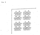
- a quartet structure formed of two green pixels, one blue pixel and one red pixel is used and fluorescent substances corresponding to the above colors are disposed on each respective discharge cell 3.
- Fig. 3 is a time chart illustrating how the intensities are produced.
- One field corresponding to a picture is divided into a plurality of sub-fields, and the intensities are produced by controlling the light emission period of each respective sub-field.
- One field is divided into 8 sub-fields, each having an equal time period, and the light emission period of each respective sub-field is assigned a different value. Pixels on each respective scan line can-be displayed in any of the 256 intensity levels by selecting the light emission period at the corresponding sub-fields.
- color image display is made possible with a plasma display by forming discharge cells 3 at the crossing points between display electrodes and scan electrodes.
- Phosphors of green, blue and red are disposed in a quartet structure and illuminated to create a color display. Varying the intensity of the display is made possible by means of the sub-fields.
- the arrangement of two green pixels disposed in the quartet structure enhances brightness and also improves the apparent display resolution. Since there are two green pixels in the quartet structure, simply supplying video signals to respective pixels of red, green and blue would disturb the white balance and reproduce excessive green colon On the other hand, supplying the green video signal with its amplitude reduced by 1/2 in order to preserve the white balance would cause the intensity to deteriorate to 128 levels due to a reduction in the signal amplitude.
- EP-A-0525750 discloses a display control apparatus which may be used with a CRT or a plasma display, wherein a pixel unit of the display is composed of two dots, and wherein the output of the two dots may be controlled to display a text data item and a graphics data item respectively.
- the object of the present invention is to provide a plasma display of high grade and good picture quality by paying a particular attention to the fact that there are two green pixels employed in the quartet type RGB dot-matrix structure, and by having the brightness enhanced and the apparent display resolution improved while maintaining a good white balance as well as a wide range of
- the present invention provides a plasma display including a plurality of pixel units, each pixel unit including two green pixels, one blue pixel and one red pixel, each of the pixels being supplied with respective green, blue and red digitised video signals, each signal being suitable for producing an integer number N of grey-level intensities and in any sample period assuming a respective first integer intensity level A wherein 1 ⁇ A ⁇ N, the plasma display comprising:-
- the present invention also provides a plasma display including a plurality of pixel units, each pixel unit including two green pixels, one blue pixel and one red pixel, each of the pixels being supplied with respective green, blue and red digitised video signals, each signal being suitable for producing an integer number N of grey-level intensities and in any sample period assuming a respective first integer intensity level A, wherein 1 ⁇ A ⁇ N, the plasma display comprising:
- the foregoing circuits make it possible to incorporate the least significant bit information, which was lost by halving the green signal value to maintain the white balance, in the halved green signal based on a timing signal, thereby realising 256 intensity levels without degrading the halftone in the video pictures.
- control signal is a logical product between the least significant bit of the digitzed green video signal and a signal obtained by dividing by two the sampling clock signal employed in digitization
- 256 levels can be realised without causing any deterioration in intensity while maintaining the average brightness within one line.
- the reference circuit generates a logical product between, an exclusive OR of a signal obtained by dividing by two the sampling clock signal employed in digitization and a signal obtained by dividing by two the horizonal synchronizing signal, and the least significant bit value of the digitized green video signals.
- the logical product is output as a control signal.
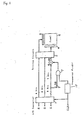
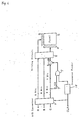
- Fig. 1 is a block diagram of a plasma display in a first embodiment of the present invention.
- Fig. 2 is a plan view of the electrode arrangements on the plasma display panel.
- Fig. 3 is a time chart for the plasma display sub-fields.
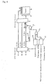
- Fig. 4 is a block diagram of a plasma display in a second embodiment of the present invention.
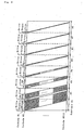
- Fig. 5 is a plan view of a panel illustrating intensities of individual pixels in the display.
- Fig. 6 is a block diagram of a plasma display in a third embodiment of the present invention.
- Fig. 7 is a block diagram of a plasma display in a fourth embodiment of the present invention.
- a plasma display and the plasma display operation will be explained with reference to specific exemplary embodiments thereof.
- Fig. 1 is a block diagram of a plasma display panel whereby video signals decoded into R, G and B, are reproduced on the display panel.
- each respective video signal of an NTSC RGB signal is converted to an 8 bit digital signal by A/D converter 1.
- a reference circuit 7 outputs as a control signal a logical product between the least significant bit (LSB) 9 of a digitized green video signal and a signal output by frequency divider 10 obtained by dividing by two the sampling clock signal used by A/D 1.
- Arithmetic circuit 8 adds or subtracts the control signal output by the reference circuit 7 to the digitized green video signal.
- a driving circuit 2 inputs digitized red and blue signals together with the output from the arithmetic circuit 8.
- Driving circuit 2 performs combinational operations based on the number of pulse times corresponding to the gray levels of 128, 64, 32, 16, 8, 4, 2 and 1 as defined in the time chart for the 8 sub-fields shown in Fig. 3.
- Signals of a driving waveform that are necessary for each respective discharge cell 3 of a display panel 6 to emit light are applied to the scan electrodes 4 and the display electrodes 5.
- video images are displayed on display panel 6.
- red (R) and blue (B) pixels within a quartet respectively present intensities corresponding to the pulse number for level 127.
- the input signal digitized by the A/D converter 1 is converted to a 7 bit signal corresponding to level 63.
- a logical product between the least significant bit value and the signal obtained by dividing by two the sampling clock that is used in digitization by the A/D converter 1 is taken.
- the control signal is a 1 when the logical product is true and a 0 when the logical product is false.
- one of the two green pixels within a quartet is adjusted to level 64 by adding one level through arithmetic circuit 8.
- the other green pixel remains at level 63.
- an average brightness level of 63.5 is realized, and the sum of the brightness levels of the two green pixels within one quartet becomes level 127 exactly.
- the logical product value output by reference circuit 7 becomes true or false in response to a signal obtained through dividing by two the sampling clock used in the A/D converter. Therefore, in each quartet shown in Fig. 5, the logical products corresponding to the green pixels at the lower right and upper left are different from one another. Thus, the total intensity of the green pixels for each respective quartet is at the correct level 127.
- the least significant bit is 0 and thus reference circuit 7 outputs 0.
- the green pixel intensities are produced according to the pulse number that corresponds to level 64 without adding or subtracting 1 from either green pixel.
- the present invention makes it possible to have the least significant bit information, which is lost by halving the green signal magnitude to maintain the white balance, reflected in the halved green signal by using a signal obtained by dividing by two the sampling clock used by A/D converter 1, thereby realizing intensities extending over 256 gray levels.
- Fig. 4 is a block diagram of a plasma display panel according to a second embodiment of the present invention whereby video signals decoded into R, G and B are reproduced on the plasma display panel.
- each NTSC red, green and blue signal is converted to a digital signal by an A/D converter 1 and fed into a driving circuit 2. Then, the signals are applied to scan electrodes 4 and display electrodes 5 to produce waveforms that are required for the display panel 6 to emit light, thereby displaying video pictures. This is the same as Example 1.
- An exclusive OR gate 12 inputs a signal output by frequency divider obtained by dividing by two the sampling clock signal used by A/D converter 1 and a signal output by frequency divider 11 obtained by dividing by two the horizontal synchronizing signal.
- the output of exclusive OR gate 12 is a control signal that controls an add operation performed by arithmetic circuit 8.
- a logical product between the least significant bit of the digitized green video signal and the exclusive OR gate 12 is obtained to produce a control signal, which is then added to the bit digitized green signal by arithmetic circuit 8.
- the upper green pixel has level 64 and the lower green pixel has level 63 in the first quartet.
- the upper green pixel has level 63 and the lower green pixel has level 64 in the second quartet, as shown in Fig. 5.
- the odd number lines and even number lines alternatively have 1 added to the green pixel level according to the condition of the horizontal synchronizing signal.
- the sum of the brightness levels of two green pixels within one quartet is level 127.
- the average brightness in the horizontal and vertical directions is uniform, the white balance is maintained, and intensities extending over 256 gray levels are all achieved at the same time.
- the plasma display of the present invention comprises a reference circuit 7 that outputs a control signal based on a value of the least significant bit 9 of a digitized green video signal and a timing signal.
- An arithmetic circuit 8 performs an arithmetic operation on the digitized green video signal and the output from the reference circuit 7.
- the least significant bit information which was lost by halving the green signal value in order to take a white balance, is incorporated in the halved green signal based on a timing signal, thereby realizing 256 intensity levels without degrading the halftone in the video picture.
- the control signal is a logical product between the least significant bit of the digitized green video signal and a signal obtained by dividing by two the sampling clock used in A/D converter 1, thereby realizing 256 intensity levels without causing any degradation in the halftone in the video picture while maintaining the average brightness within one line.
- control signal is a logical product between an exclusive OR of a signal obtained by dividing by two the sampling clock used by A/D converter 1 and a signal obtained by dividing by two the horizontal synchronizing signal, and the least significant bit of the digitized green video signal.
- the plasma displays of Examples 1 and 2 are easy to manufacture and cost effective, and will make valuable contributions to the industry.
Landscapes
- Engineering & Computer Science (AREA)
- Physics & Mathematics (AREA)
- Plasma & Fusion (AREA)
- Computer Hardware Design (AREA)
- General Physics & Mathematics (AREA)
- Theoretical Computer Science (AREA)
- Control Of Indicators Other Than Cathode Ray Tubes (AREA)
- Processing Of Color Television Signals (AREA)
- Control Of Gas Discharge Display Tubes (AREA)
- Dairy Products (AREA)
Claims (6)
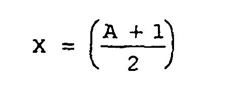
- Affichage à plasma comprenant une pluralité d'unités d'éléments d'image, chaque unité d'éléments d'image comprenant deux éléments d'image verts, un élément d'image bleu et un élément d'image rouge, chacun des éléments d'image recevant des signaux vidéo numérisés vert, bleu et rouge, respectifs, chaque signal étant approprié pour produire un nombre entier N d'intensités de niveaux de gris et dans une période d'échantillons quelconque supposant un premier niveau d'intensité entier respectif A dans lequel 1 ≤ A ≤ N, l'affichage à plasma comprenant :un circuit de référence (7) pour délivrer en tant que signal de commande un produit logique ET entre le bit de plus faible poids d'un signal vidéo vert numérisé et un signal de synchronisation obtenu en divisant (10) par deux la fréquence du signal d'horloge d'échantillonnage (CLK) utilisé dans la numérisation, le signal vert numérisé étant converti en un signal vert numérisé converti approprié pour produire un second niveau d'intensité entier X, dans lequel si A est impair, alorsautrement si A est pair, alors

 un circuit arithmétique (8) pour additionner le signal de commande au signal vert numérisé converti : etun circuit d'excitation (2) agencé pour recevoir les signaux vidéo rouge et bleu numérisés conjointement avec le signal vidéo vert numérisé converti délivré par ledit circuit arithmétique, et étant en outre agencé pour exciter un desdits deux éléments d'image verts dans chaque unité d'élément d'image conformément audit signal vidéo vert numérisé converti et l'autre desdits deux éléments d'image verts dans chaque unité conformément audit signal vidéo vert numérisé converti réglé selon une valeur du signal de commande.
 - Affichage à plasma selon la revendication 1, dans lequel ledit circuit arithmétique est un circuit d'addition agencé pour additionner 1 au signal vidéo numérisé dudit autre des deux éléments d'image verts dans chaque unité d'éléments d'image selon le bit de plus faible poids du signal vert numérisé.
- Affichage à plasma comprenant une pluralité d'unités d'éléments d'image, chaque unité d'éléments d'image comprenant deux éléments d'image verts, un élément d'image bleu et un élément d'image rouge, chacun des éléments d'image recevant des signaux vidéo vert, bleu et rouge numérisés respectifs, chaque signal étant approprié pour produire un nombre entier N d'intensités de niveau de gris et dans une période d'échantillon quelconque supposant un premier niveau d'intensité entier respectif A, dans lequel 1 ≤ A ≤ N, l'affichage à plasma comprenant :un circuit de référence (7) pour délivrer en tant que signal de commande un produit logique ET entre le bit de plus faible poids d'un signal vidéo vert numérisé et d'un signal de synchronisation obtenu en divisant (10) par deux la fréquence du signal d'horloge d'échantillonnage (CLK) utilisé dans la numérisation, le signal vert numérisé étant converti en un signal vert numérisé converti approprié pour produire un second niveau d'intensité entier X, dans lequel si A est impair, alorsautrement si A est pair, alors
 un circuit arithmétique (8) pour retrancher le signal de commande du signal vert numérisé converti ; etun circuit d'excitation (2) agencé pour recevoir les signaux vidéo rouge et bleu numérisés conjointement avec le signal vidéo vert numérisé converti délivré par ledit circuit arithmétique, et étant en outre converti pour exciter l'un desdits deux éléments d'image verts dans chaque unité d'éléments d'image conformément audit signal vidéo vert numérisé converti et l'autre desdits deux éléments d'image verts dans chaque unité conformément audit signal vidéo vert numérisé converti réglé selon une valeur du signal de commande.
 - Affichage à plasma selon la revendication 3, dans lequel ledit circuit arithmétique est un circuit de soustraction agencé pour retrancher 1 du signal vidéo numérisé dudit autre des deux éléments d'image verts dans chaque circuit selon le bit de plus faible poids du signal vert numérisé.
- Affichage à plasma selon l'une quelconque des revendications précédentes, dans lequel le signal d'horloge d'échantillonnage est utilisé pour numériser les signaux vidéo rouge, bleu et vert.
- Affichage à plasma selon l'une quelconque des revendications précédentes, dans lequel ledit signal de synchronisation est en outre obtenu par un OU exclusif (11) dudit signal d'horloge d'échantillonnage divisé par deux, et un autre signal obtenu en divisant par deux un signal de synchronisation horizontale.
Applications Claiming Priority (3)
| Application Number | Priority Date | Filing Date | Title |
|---|---|---|---|
| JP26533094A JP3309593B2 (ja) | 1994-10-28 | 1994-10-28 | プラズマディスプレイ |
| JP26533094 | 1994-10-28 | ||
| JP265330/94 | 1994-10-28 |
Publications (2)
| Publication Number | Publication Date |
|---|---|
| EP0709821A1 EP0709821A1 (fr) | 1996-05-01 |
| EP0709821B1 true EP0709821B1 (fr) | 2001-11-14 |
Family
ID=17415695
Family Applications (1)
| Application Number | Title | Priority Date | Filing Date |
|---|---|---|---|
| EP95306949A Expired - Lifetime EP0709821B1 (fr) | 1994-10-28 | 1995-09-29 | Dispositif d'affichage à plasma avec module de pixel de RGBG quadruplet et son circuit d'excitation |
Country Status (5)
| Country | Link |
|---|---|
| US (2) | US5856823A (fr) |
| EP (1) | EP0709821B1 (fr) |
| JP (1) | JP3309593B2 (fr) |
| CA (1) | CA2161491C (fr) |
| DE (1) | DE69523861T2 (fr) |
Families Citing this family (20)
| Publication number | Priority date | Publication date | Assignee | Title |
|---|---|---|---|---|
| KR970076451A (ko) * | 1996-05-13 | 1997-12-12 | 가나이 츠토무 | 디스플레이장치 및 표시방법 |
| KR980010984A (ko) * | 1996-07-02 | 1998-04-30 | 구자홍 | 플라즈마 표시장치의 화이트 밸런스 구현방법 |
| JP3179036B2 (ja) * | 1996-10-14 | 2001-06-25 | 三菱電機株式会社 | ディスプレイ装置 |
| US6289252B1 (en) * | 1998-08-31 | 2001-09-11 | Fisher-Rosemount Systems, Inc. | Distributed batch processing system and methods |
| KR100517365B1 (ko) * | 1998-12-01 | 2005-11-25 | 엘지전자 주식회사 | 플라즈마 표시 패널의 오차 확산 처리 회로 |
| KR100517367B1 (ko) * | 1998-12-01 | 2005-11-25 | 엘지전자 주식회사 | 플라즈마 표시 패널의 오차 확산 처리 회로 |
| KR100517366B1 (ko) * | 1998-12-01 | 2005-11-25 | 엘지전자 주식회사 | 플라즈마 표시 패널의 오차 확산 처리 회로 |
| JP3939066B2 (ja) * | 2000-03-08 | 2007-06-27 | 富士通日立プラズマディスプレイ株式会社 | カラープラズマディスプレイ装置 |
| JP4633920B2 (ja) * | 2000-12-14 | 2011-02-16 | 株式会社日立製作所 | 表示装置および表示方法 |
| DE10123235A1 (de) * | 2001-05-12 | 2002-11-14 | Philips Corp Intellectual Pty | Plasmafarbbildschirm mit Pixelmatrix-Array |
| DE10158541A1 (de) * | 2001-11-29 | 2003-06-12 | Siemens Ag | Schaltungsanordnung zur Ansteuerung eines monochromen Flachbildschirms und Verfahren zur Verminderung der Wolkigkeit eines monochromen Flachbildschirms sowie Flachbildschirm |
| JP3982249B2 (ja) * | 2001-12-11 | 2007-09-26 | 株式会社日立製作所 | 表示装置 |
| KR20030067930A (ko) * | 2002-02-09 | 2003-08-19 | 엘지전자 주식회사 | 플라즈마 디스플레이 패널의 화이트 밸런스 보상방법 및장치 |
| KR100441508B1 (ko) * | 2002-05-20 | 2004-07-23 | 삼성전자주식회사 | 화이트 밸런스 조정 장치 및 그 방법 |
| KR100436715B1 (ko) * | 2002-11-04 | 2004-06-22 | 삼성에스디아이 주식회사 | 영상의 재현성을 증진시키기 위한 영상 데이터의 고속처리 방법 |
| TWI260569B (en) * | 2003-01-29 | 2006-08-21 | Chunghwa Picture Tubes Ltd | Plasma display panel with color space transformation device |
| TW594822B (en) * | 2003-01-29 | 2004-06-21 | Chunghwa Picture Tubes Ltd | Plasma display panel with gray level white balance device |
| KR100637240B1 (ko) | 2005-08-27 | 2006-10-23 | 삼성에스디아이 주식회사 | 효율적인 화소 구조를 가진 디스플레이 패널 및 그 구동방법 |
| KR100816187B1 (ko) * | 2006-11-21 | 2008-03-21 | 삼성에스디아이 주식회사 | 플라즈마 디스플레이 장치 및 그것의 영상 처리 방법 |
| US20100271409A1 (en) * | 2008-10-20 | 2010-10-28 | Hiroyasu Makino | Image display apparatus, color signal correction apparatus, and color signal correction method |
Family Cites Families (20)
| Publication number | Priority date | Publication date | Assignee | Title |
|---|---|---|---|---|
| US3833031A (en) * | 1970-10-30 | 1974-09-03 | P Fechtheimer | Filling machine for containers |
| US3969995A (en) * | 1973-08-13 | 1976-07-20 | Kraftco Corporation | Apparatus for making large sized blocks of cheese |
| US4018145A (en) * | 1974-08-19 | 1977-04-19 | Hensel Otis O | Apparatus for draining whey from cheese |
| GB1494509A (en) * | 1975-02-17 | 1977-12-07 | Miller M | Plasma display control apparatus |
| GB1541836A (en) * | 1975-04-04 | 1979-03-07 | Wincanton Eng | Drainage plates for cheese moulds |
| US4244286A (en) * | 1978-02-21 | 1981-01-13 | Universal Foods Corporation | Apparatus and method for making cheese |
| US4436518A (en) * | 1980-09-15 | 1984-03-13 | Buss David L | Metal trough |
| US4520969A (en) * | 1983-10-17 | 1985-06-04 | Minnesota Mining And Manufacturing Company | Videocassette tape spool having a wear button |
| US4564156A (en) * | 1984-06-15 | 1986-01-14 | Minnesota Mining And Manufacturing Company | Videocassette wear button |
| US4752046A (en) * | 1986-06-10 | 1988-06-21 | Minnesota Mining And Manufacturing Company | Videocassette tape spool having a wear button |
| GB8707313D0 (en) * | 1987-03-26 | 1987-04-29 | Alfa Lavel Cheese Systems Ltd | Cheese block former |
| US5341153A (en) * | 1988-06-13 | 1994-08-23 | International Business Machines Corporation | Method of and apparatus for displaying a multicolor image |
| JP2932686B2 (ja) * | 1990-11-28 | 1999-08-09 | 日本電気株式会社 | プラズマディスプレイパネルの駆動方法 |
| US5170152A (en) * | 1990-12-14 | 1992-12-08 | Hewlett-Packard Company | Luminance balanced encoder |
| US5177656A (en) * | 1991-02-05 | 1993-01-05 | Hoechst Celanese Corporation | Flexible magnetic disc cassettes with integrally molded wear button |
| US5479189A (en) * | 1991-02-28 | 1995-12-26 | Chesavage; Jay | 4 channel color display adapter and method for color correction |
| EP0525750A3 (en) * | 1991-07-30 | 1995-03-22 | Tokyo Shibaura Electric Co | Display control apparatus |
| US5469190A (en) * | 1991-12-23 | 1995-11-21 | Apple Computer, Inc. | Apparatus for converting twenty-four bit color to fifteen bit color in a computer output display system |
| GB2280603B (en) * | 1993-08-03 | 1996-08-07 | Btr Plc | Floor coverings |
| CA2105460C (fr) * | 1993-09-02 | 1996-10-15 | France Delisle | Vitrages isolants multi-couches et materiaux assimiles, et separateur isolant connexe |
-
1994
- 1994-10-28 JP JP26533094A patent/JP3309593B2/ja not_active Expired - Fee Related
-
1995
- 1995-09-14 US US08/528,019 patent/US5856823A/en not_active Expired - Fee Related
- 1995-09-14 US US08/528,017 patent/US5630361A/en not_active Expired - Lifetime
- 1995-09-29 EP EP95306949A patent/EP0709821B1/fr not_active Expired - Lifetime
- 1995-09-29 DE DE69523861T patent/DE69523861T2/de not_active Expired - Fee Related
- 1995-10-26 CA CA002161491A patent/CA2161491C/fr not_active Expired - Fee Related
Also Published As
| Publication number | Publication date |
|---|---|
| JPH08123366A (ja) | 1996-05-17 |
| CA2161491C (fr) | 2005-06-07 |
| EP0709821A1 (fr) | 1996-05-01 |
| DE69523861D1 (de) | 2001-12-20 |
| US5630361A (en) | 1997-05-20 |
| CA2161491A1 (fr) | 1996-04-29 |
| US5856823A (en) | 1999-01-05 |
| JP3309593B2 (ja) | 2002-07-29 |
| DE69523861T2 (de) | 2002-04-18 |
Similar Documents
| Publication | Publication Date | Title |
|---|---|---|
| EP0709821B1 (fr) | Dispositif d'affichage à plasma avec module de pixel de RGBG quadruplet et son circuit d'excitation | |
| US6518977B1 (en) | Color image display apparatus and method | |
| US7176867B2 (en) | Liquid crystal display and driving method thereof | |
| US6714250B1 (en) | Method and apparatus for processing video pictures, in particular for large area flicker effect reduction | |
| KR100454786B1 (ko) | 텔레비젼화상신호의계조표시방법및그장치 | |
| US6476824B1 (en) | Luminance resolution enhancement circuit and display apparatus using same | |
| KR100435082B1 (ko) | 액정 표시 장치 | |
| US6825835B2 (en) | Display device | |
| KR0147296B1 (ko) | 액정 디스플레이에 상이한 색조의 회색을 디스플레이하기 위한 장치 및 그 방법 | |
| US7184053B2 (en) | Method for processing video data for a display device | |
| KR100312362B1 (ko) | 불량동화상윤곽을보정하면서동화상을디스플레이하는방법및장치 | |
| JPH07175439A (ja) | ディスプレイ装置の駆動方法 | |
| EP0982708A1 (fr) | Méthode et appareil de traitement d'images vidéo, en particulier pour la réduction du scintillement de grande surface | |
| US6741227B2 (en) | Color image display apparatus and method | |
| US6151000A (en) | Display apparatus and display method thereof | |
| US7277105B2 (en) | Drive control apparatus and method for matrix panel | |
| EP1446790B1 (fr) | Systeme et procede destine a reguler l'intensite d'un pixel | |
| KR19980066488A (ko) | 다계조 처리장치 | |
| JP2002323872A (ja) | プラズマディスプレイパネルの駆動方法及びプラズマ表示装置 | |
| JP3002490B2 (ja) | 駆動回路,表示装置及び表示方法 | |
| JPH10105108A (ja) | カラー画像表示装置 | |
| US7079089B2 (en) | Gray display method and device for plasma display panel | |
| KR100292535B1 (ko) | 플라즈마표시장치의구동방법및장치 | |
| JPH07219493A (ja) | ディスプレイ装置の中間調表示回路 | |
| KR100965577B1 (ko) | 액정표시장치 및 이의 구동방법 |
Legal Events
| Date | Code | Title | Description |
|---|---|---|---|
| PUAI | Public reference made under article 153(3) epc to a published international application that has entered the european phase |
Free format text: ORIGINAL CODE: 0009012 |
|
| AK | Designated contracting states |
Kind code of ref document: A1 Designated state(s): DE FR GB |
|
| 17P | Request for examination filed |
Effective date: 19960712 |
|
| 17Q | First examination report despatched |
Effective date: 19990105 |
|
| RTI1 | Title (correction) |
Free format text: PLASMA DISPLAY WITH PIXEL UNITS COMPRISED OF AN RGBG QUARTET, AND A DRIVING APPARATUS THEREFOR |
|
| GRAG | Despatch of communication of intention to grant |
Free format text: ORIGINAL CODE: EPIDOS AGRA |
|
| RTI1 | Title (correction) |
Free format text: PLASMA DISPLAY WITH PIXEL UNITS COMPRISED OF AN RGBG QUARTET, AND A DRIVING APPARATUS THEREFOR |
|
| RTI1 | Title (correction) |
Free format text: PLASMA DISPLAY WITH PIXEL UNITS COMPRISED OF AN RGBG QUARTET, AND A DRIVING APPARATUS THEREFOR |
|
| GRAG | Despatch of communication of intention to grant |
Free format text: ORIGINAL CODE: EPIDOS AGRA |
|
| GRAG | Despatch of communication of intention to grant |
Free format text: ORIGINAL CODE: EPIDOS AGRA |
|
| GRAH | Despatch of communication of intention to grant a patent |
Free format text: ORIGINAL CODE: EPIDOS IGRA |
|
| GRAH | Despatch of communication of intention to grant a patent |
Free format text: ORIGINAL CODE: EPIDOS IGRA |
|
| GRAA | (expected) grant |
Free format text: ORIGINAL CODE: 0009210 |
|
| AK | Designated contracting states |
Kind code of ref document: B1 Designated state(s): DE FR GB |
|
| REF | Corresponds to: |
Ref document number: 69523861 Country of ref document: DE Date of ref document: 20011220 |
|
| REG | Reference to a national code |
Ref country code: GB Ref legal event code: IF02 |
|
| PLBE | No opposition filed within time limit |
Free format text: ORIGINAL CODE: 0009261 |
|
| STAA | Information on the status of an ep patent application or granted ep patent |
Free format text: STATUS: NO OPPOSITION FILED WITHIN TIME LIMIT |
|
| 26N | No opposition filed | ||
| PGFP | Annual fee paid to national office [announced via postgrant information from national office to epo] |
Ref country code: DE Payment date: 20070927 Year of fee payment: 13 |
|
| PGFP | Annual fee paid to national office [announced via postgrant information from national office to epo] |
Ref country code: GB Payment date: 20070926 Year of fee payment: 13 |
|
| PGFP | Annual fee paid to national office [announced via postgrant information from national office to epo] |
Ref country code: FR Payment date: 20070914 Year of fee payment: 13 |
|
| GBPC | Gb: european patent ceased through non-payment of renewal fee |
Effective date: 20080929 |
|
| REG | Reference to a national code |
Ref country code: FR Ref legal event code: ST Effective date: 20090529 |
|
| PG25 | Lapsed in a contracting state [announced via postgrant information from national office to epo] |
Ref country code: DE Free format text: LAPSE BECAUSE OF NON-PAYMENT OF DUE FEES Effective date: 20090401 |
|
| PG25 | Lapsed in a contracting state [announced via postgrant information from national office to epo] |
Ref country code: FR Free format text: LAPSE BECAUSE OF NON-PAYMENT OF DUE FEES Effective date: 20080930 |
|
| PG25 | Lapsed in a contracting state [announced via postgrant information from national office to epo] |
Ref country code: GB Free format text: LAPSE BECAUSE OF NON-PAYMENT OF DUE FEES Effective date: 20080929 |