EP0709822A2 - Verbesserungen an oder im Zusammenhang mit Datenformatiereinrichtungen und Bildspeichern - Google Patents
Verbesserungen an oder im Zusammenhang mit Datenformatiereinrichtungen und Bildspeichern Download PDFInfo
- Publication number
- EP0709822A2 EP0709822A2 EP95117187A EP95117187A EP0709822A2 EP 0709822 A2 EP0709822 A2 EP 0709822A2 EP 95117187 A EP95117187 A EP 95117187A EP 95117187 A EP95117187 A EP 95117187A EP 0709822 A2 EP0709822 A2 EP 0709822A2
- Authority
- EP
- European Patent Office
- Prior art keywords
- data
- bit
- reformatter
- memory
- words
- Prior art date
- Legal status (The legal status is an assumption and is not a legal conclusion. Google has not performed a legal analysis and makes no representation as to the accuracy of the status listed.)
- Withdrawn
Links
Images

Classifications
-
- G—PHYSICS
- G09—EDUCATION; CRYPTOGRAPHY; DISPLAY; ADVERTISING; SEALS
- G09G—ARRANGEMENTS OR CIRCUITS FOR CONTROL OF INDICATING DEVICES USING STATIC MEANS TO PRESENT VARIABLE INFORMATION
- G09G3/00—Control arrangements or circuits, of interest only in connection with visual indicators other than cathode-ray tubes
- G09G3/20—Control arrangements or circuits, of interest only in connection with visual indicators other than cathode-ray tubes for presentation of an assembly of a number of characters, e.g. a page, by composing the assembly by combination of individual elements arranged in a matrix no fixed position being assigned to or needed to be assigned to the individual characters or partial characters
- G09G3/2092—Details of a display terminals using a flat panel, the details relating to the control arrangement of the display terminal and to the interfaces thereto
-
- G—PHYSICS
- G06—COMPUTING OR CALCULATING; COUNTING
- G06K—GRAPHICAL DATA READING; PRESENTATION OF DATA; RECORD CARRIERS; HANDLING RECORD CARRIERS
- G06K15/00—Arrangements for producing a permanent visual presentation of the output data, e.g. computer output printers
- G06K15/02—Arrangements for producing a permanent visual presentation of the output data, e.g. computer output printers using printers
- G06K15/12—Arrangements for producing a permanent visual presentation of the output data, e.g. computer output printers using printers by photographic printing, e.g. by laser printers
- G06K15/1238—Arrangements for producing a permanent visual presentation of the output data, e.g. computer output printers using printers by photographic printing, e.g. by laser printers simultaneously exposing more than one point
- G06K15/1242—Arrangements for producing a permanent visual presentation of the output data, e.g. computer output printers using printers by photographic printing, e.g. by laser printers simultaneously exposing more than one point on one main scanning line
- G06K15/1252—Arrangements for producing a permanent visual presentation of the output data, e.g. computer output printers using printers by photographic printing, e.g. by laser printers simultaneously exposing more than one point on one main scanning line using an array of light modulators, e.g. a linear array
-
- G—PHYSICS
- G09—EDUCATION; CRYPTOGRAPHY; DISPLAY; ADVERTISING; SEALS
- G09G—ARRANGEMENTS OR CIRCUITS FOR CONTROL OF INDICATING DEVICES USING STATIC MEANS TO PRESENT VARIABLE INFORMATION
- G09G3/00—Control arrangements or circuits, of interest only in connection with visual indicators other than cathode-ray tubes
- G09G3/20—Control arrangements or circuits, of interest only in connection with visual indicators other than cathode-ray tubes for presentation of an assembly of a number of characters, e.g. a page, by composing the assembly by combination of individual elements arranged in a matrix no fixed position being assigned to or needed to be assigned to the individual characters or partial characters
- G09G3/2007—Display of intermediate tones
- G09G3/2018—Display of intermediate tones by time modulation using two or more time intervals
- G09G3/2022—Display of intermediate tones by time modulation using two or more time intervals using sub-frames
-
- H—ELECTRICITY
- H04—ELECTRIC COMMUNICATION TECHNIQUE
- H04N—PICTORIAL COMMUNICATION, e.g. TELEVISION
- H04N1/00—Scanning, transmission or reproduction of documents or the like, e.g. facsimile transmission; Details thereof
- H04N1/04—Scanning arrangements, i.e. arrangements for the displacement of active reading or reproducing elements relative to the original or reproducing medium, or vice versa
- H04N1/19—Scanning arrangements, i.e. arrangements for the displacement of active reading or reproducing elements relative to the original or reproducing medium, or vice versa using multi-element arrays
- H04N1/1903—Arrangements for enabling electronic abutment of lines or areas independently scanned by different elements of an array or by different arrays
-
- H—ELECTRICITY
- H04—ELECTRIC COMMUNICATION TECHNIQUE
- H04N—PICTORIAL COMMUNICATION, e.g. TELEVISION
- H04N1/00—Scanning, transmission or reproduction of documents or the like, e.g. facsimile transmission; Details thereof
- H04N1/04—Scanning arrangements, i.e. arrangements for the displacement of active reading or reproducing elements relative to the original or reproducing medium, or vice versa
- H04N1/19—Scanning arrangements, i.e. arrangements for the displacement of active reading or reproducing elements relative to the original or reproducing medium, or vice versa using multi-element arrays
- H04N1/191—Scanning arrangements, i.e. arrangements for the displacement of active reading or reproducing elements relative to the original or reproducing medium, or vice versa using multi-element arrays the array comprising a one-dimensional [1D] array
- H04N1/192—Simultaneously or substantially simultaneously scanning picture elements on one main scanning line
- H04N1/193—Simultaneously or substantially simultaneously scanning picture elements on one main scanning line using electrically scanned linear arrays, e.g. linear CCD arrays
- H04N1/1934—Combination of arrays
-
- H—ELECTRICITY
- H04—ELECTRIC COMMUNICATION TECHNIQUE
- H04N—PICTORIAL COMMUNICATION, e.g. TELEVISION
- H04N21/00—Selective content distribution, e.g. interactive television or video on demand [VOD]
- H04N21/40—Client devices specifically adapted for the reception of or interaction with content, e.g. set-top-box [STB]; Operations thereof
- H04N21/41—Structure of client; Structure of client peripherals
- H04N21/426—Internal components of the client ; Characteristics thereof
-
- H—ELECTRICITY
- H04—ELECTRIC COMMUNICATION TECHNIQUE
- H04N—PICTORIAL COMMUNICATION, e.g. TELEVISION
- H04N5/00—Details of television systems
- H04N5/74—Projection arrangements for image reproduction, e.g. using eidophor
- H04N5/7416—Projection arrangements for image reproduction, e.g. using eidophor involving the use of a spatial light modulator, e.g. a light valve, controlled by a video signal
- H04N5/7458—Projection arrangements for image reproduction, e.g. using eidophor involving the use of a spatial light modulator, e.g. a light valve, controlled by a video signal the modulator being an array of deformable mirrors, e.g. digital micromirror device [DMD]
-
- H—ELECTRICITY
- H04—ELECTRIC COMMUNICATION TECHNIQUE
- H04N—PICTORIAL COMMUNICATION, e.g. TELEVISION
- H04N7/00—Television systems
- H04N7/01—Conversion of standards, e.g. involving analogue television standards or digital television standards processed at pixel level
-
- G—PHYSICS
- G06—COMPUTING OR CALCULATING; COUNTING
- G06K—GRAPHICAL DATA READING; PRESENTATION OF DATA; RECORD CARRIERS; HANDLING RECORD CARRIERS
- G06K2215/00—Arrangements for producing a permanent visual presentation of the output data
- G06K2215/111—Arrangements for producing a permanent visual presentation of the output data with overlapping swaths
-
- G—PHYSICS
- G09—EDUCATION; CRYPTOGRAPHY; DISPLAY; ADVERTISING; SEALS
- G09G—ARRANGEMENTS OR CIRCUITS FOR CONTROL OF INDICATING DEVICES USING STATIC MEANS TO PRESENT VARIABLE INFORMATION
- G09G2310/00—Command of the display device
- G09G2310/02—Addressing, scanning or driving the display screen or processing steps related thereto
- G09G2310/0264—Details of driving circuits
- G09G2310/027—Details of drivers for data electrodes, the drivers handling digital grey scale data, e.g. use of D/A converters
-
- G—PHYSICS
- G09—EDUCATION; CRYPTOGRAPHY; DISPLAY; ADVERTISING; SEALS
- G09G—ARRANGEMENTS OR CIRCUITS FOR CONTROL OF INDICATING DEVICES USING STATIC MEANS TO PRESENT VARIABLE INFORMATION
- G09G2340/00—Aspects of display data processing
- G09G2340/04—Changes in size, position or resolution of an image
- G09G2340/0492—Change of orientation of the displayed image, e.g. upside-down, mirrored
-
- G—PHYSICS
- G09—EDUCATION; CRYPTOGRAPHY; DISPLAY; ADVERTISING; SEALS
- G09G—ARRANGEMENTS OR CIRCUITS FOR CONTROL OF INDICATING DEVICES USING STATIC MEANS TO PRESENT VARIABLE INFORMATION
- G09G2360/00—Aspects of the architecture of display systems
- G09G2360/18—Use of a frame buffer in a display terminal, inclusive of the display panel
-
- H—ELECTRICITY
- H04—ELECTRIC COMMUNICATION TECHNIQUE
- H04N—PICTORIAL COMMUNICATION, e.g. TELEVISION
- H04N5/00—Details of television systems
- H04N5/74—Projection arrangements for image reproduction, e.g. using eidophor
- H04N5/7416—Projection arrangements for image reproduction, e.g. using eidophor involving the use of a spatial light modulator, e.g. a light valve, controlled by a video signal
- H04N5/7458—Projection arrangements for image reproduction, e.g. using eidophor involving the use of a spatial light modulator, e.g. a light valve, controlled by a video signal the modulator being an array of deformable mirrors, e.g. digital micromirror device [DMD]
- H04N2005/7466—Control circuits therefor
Definitions
- This invention relates to the field of display systems, more particularly to image data manipulation circuits used in digital television display systems.
- Display systems such as televisions display full-motion video images as a series of still frames.
- Each frame of the image is comprised of a two-dimensional array of picture elements, known as pixels, arranged in orthogonal rows and columns.
- the image information is transmitted in a raster-scan format, one line at a time from top to bottom. Within each line the pixel information is transmitted from left to right.
- Standard television systems in the United States have 480 rows with a resolution of approximately 572 pixels in each row.
- Video Graphic Adapter (VGA) standards specify an image comprised of 480 rows of 640 pixels.
- Wide-NTSC television standards specify an image 853 pixels wide and 480 rows high. While there is no universally accepted standard for high-definition television, some formats display up to 1152 rows with 2048 columns.
- Analog display devices such as cathode ray tubes (CRT) accept raster-scan image data and project it onto the display screen in real-time, one line at a time as it is received.
- CTR cathode ray tubes
- many digital display systems require the data to be displayed an entire screen at a time. This requires the data to be stored as it is received until all the data for a given screen is ready to be displayed.
- An efficient data storage means is one aspect of this invention.
- image data transfer has referred to the image data for a single pixel as an indivisible unit.
- digital display systems require image data that is comprised of one or more weighted binary bits.
- Digital systems that have more than one bit of image data typically transmit all bits for a given pixel in parallel. For example, a three color display having eight bits of data for each color typically transmits one 24-bit-wide word for each pixel. If the digital display pixel can only display one bit at a time, each of the 24 bits must be displayed sequentially in order to create the desired intensity level and color for the pixel.
- One method of generating the required "gray scale" is pulse width modulation as described in commonly assigned US Patent No. 5,278,562 entitled “DMD Architecture and Timing for use in a Pulse-Width Modulated Display System.”
- the 8-bit image is displayed as a series of 8 1-bit images or "bit planes.”
- Each bit plane is displayed for a period of time that is directly related to the significance of the bit. For example, a bit plane comprised of the most significant bit from each of the data words representing a pixel is extracted and displayed for a period of time. A second bit plane, comprised of the next most significant bit from each data word is then extracted and displayed for a period of time half as long as the first period. This process continues until each bit in the data word has been displayed.
- the image data is received as a serial stream of pixels, with each pixel comprised of parallel data bits, and displayed as a serial stream of bit planes, with each bit plane comprised of one data bit for each pixel.
- a data reformatter/frame memory that provides an efficient means of performing an orthogonal reordering of data pixels.
- the data reformatter allows the conversion of a stream of first data words into a stream of second data words wherein each second data word contains one bit from each of the first data words.
- the disclosed frame memory stores the stream of second data words until the data words are required for display.
- the data reformatter includes at least one reformatter memory plane which includes an m x n array of memory cells for receiving and storing m n-bit-wide input data words from an input bus, and for outputting n m-bit-wide output data words to an output data bus.
- the m-bit-wide output data words are comprised of one bit from each of the m n-bit-wide input data words.
- a display system is comprised of a data reformatter, a display device, and a controller for coordinating the operation of the data reformatter and the display device.
- the data reformatter is comprised of an m x n array of memory cells for receiving and storing m n-bit-wide input data words, and for outputting n m-bit-wide output data words.
- the m-bit-wide output data words are comprised of one bit from each of the m n-bit-wide input data words.
- the disclosed data reformatter/frame memory enables the processing of video data wherein m n-bit input data words are written into a reformatter memory, and n m-bit output data words, each comprised of one bit from each of the input data words, are read out of the reformatter memory.
- the n m-bit output data words are typically stored in a frame memory until the data is displayed.
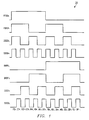
- Figure 1 depicts 8 waveforms 20 representing a series of 8-bit binary image data words for a row of sixteen pixels.
- the image data for the 16 pixels would be transmitted as the series of 16 8-bit data words shown beneath the waveforms of Figure 1. As discussed above, data of a given bit significance for all pixels in a row is input into a digital display simultaneously.
- the image data shown in Figure 1 is received as a series of 16 8-bit words, F0h, E1h, D2h, C3h, B4h, A5h, 96h, 87h, 78h, 69h, 5Ah, 4Bh, 3Ch, 2Dh, 1Eh, 0Fh, but is loaded into the display device as a series of 8 16-bit words FF00h, F0F0h, 3333h, 5555h, 00FFh, 0F0Fh, 3333h, 5555h.
- orthogonal reordering One function of the reformatter memory disclosed herein is to perform the orthogonal reordering by receiving a data stream from a video source in one format, and changing the order that the data bits are output to the order required by the display device.
- Figure 2 One method of achieving this reordering is shown in Figure 2.
- each word is written into a separate register.
- the data word for pixel 1 is written into register 42
- the second word is written into register 44
- the sixteenth word is written into register 48.
- the data is read out of the reformatter 40 and stored in a frame memory.
- Figure 2 shows a multiplexer 56 that is used to select which bit from each of the 16 registers to be output to the frame memory. If the outputs of the registers could be individually enabled, the outputs of each register could be interconnected and the multiplexer 56 would be unnecessary.
- Figure 2 illustrates only the mechanics of data reformatting, there are other possible circuits that perform the same function. For example, rather than use registers and a multiplexer 56, standard RAM cells could be used with orthogonal read and write enable signals.
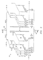
- FIG. 3 is a schematic view of another embodiment of a data reformatter circuit 59.
- each data word is 24 bits wide and contains 8 bits of intensity data for each of 3 colors.
- the reformatter circuit 59 shown in Figure 3 is designed to reformat the data for a wide-NTSC image.
- a modulator with a horizontal resolution of 864 pixels will be used to display the 853-pixel wide-NTSC image. Because 864 is a multiple of 16, the digital processing circuitry may be simplified by adding an extra 11 pixels.
- the extra 11 pixels in each row may be used to center the displayed image and to simplify the circuitry required to change from front to rear image projection.
- the reformatter illustrated in Figure 3 holds image data for two rows of 864 (32x27) pixels. Data for one row of pixels is written into half of the reformatter 61 while data for the other row is being read out of the other half of the reformatter 63. Each half of the data reformatter 61, 63 is comprised of 32 individual memory planes 60, 62, 64, 66, each of which reformats the video data words for 27 pixels. One data word for each pixel in a row is written into the memory planes 60, 62, 64, 66 at a time. Data for pixels 1 through 27 is written into memory plane 60.
- Plane 62 holds data for pixels 28 through 54.
- Plane 66 holds data for pixels 838 through 864.
- switch 68 After writing one row of data to the first half of the reformatter 61, switch 68 directs the second row of data into the second half of the reformatter 63 while switch 70 allows the first row of data to be read from the first half of the reformatter 61.
- Data is read from the reformatter 59 in 24 words that are 864 bits wide. Each word contains 27 bits from each of the 32 memory planes in the reformatter memory and is comprised of the same weight bit from every pixel in a row.
- An array of 32 27-bit registers 72, 74 at the output of each half of the reformatter 61, 63 latches the reformatted output data. After one read cycle, in which all of the image data for one weight value is read out, switch 76 is incremented to select the next bit value to be output. Because data is written into the reformatter 59 in 24-bit words and read out of the reformatter 59 in 864-bit words, filling the reformatter requires 864 write cycles but emptying the reformatter only requires 24 read cycles.
- One feature of the disclosed data reformatter 59 is the ability to pass data through the reformatter 59 without reformatting the data. This feature simplifies fault isolation between the data reformatter 59 and a frame storage memory used to store the reformatted output data.
- the input busses to the data reformatter memory planes 60, 62, 64, 66 are 27 bits wide. When the data reformatter 59 is in a reformat mode, only 24-bit data words are written into the data reformatter 59 leaving the remaining 3 bus lines unused. When the data reformatter 59 is in a test mode, 27-bit data words are written into the data reformatter 59.
- the 27 input lines are connected to the 27 output lines from each memory plane 60, 62, 64, 66 allowing the test data to be written directly into the output register array 72, 74 without first being stored by the memory planes 60, 62, 64, 66.
- all 32 of the 27-bit output registers in an array 72, 74 are latched simultaneously.
- the registers may be individually latched to allow unique data to be written into each of the registers.
- the sizes of the data words and reformatter memories used in the above description were selected for illustrative purposes. For example, one embodiment may use only 16 memory planes 60, 62, 64, 66 instead of the 32 memory planes 60, 62, 64, 66 described above. This would reduce the capacity of each half of the reformatter 61, 63 from one line of data to one-half line of data.
- the output word from the reformatter 59 would be 432 bits wide and contain one bit of data for half of the pixels in a row.
- a data reformatter 59 designed for use in a VGA compatible display system may contain only 10 memory planes 60, 62, 64, 60, each of which holds 32 24-bit words, enabling each half of the reformatter 61, 63 to contain all of the data for one-half of a row of 640 pixels.
- Another feature of the disclosed reformatter 59 is the ability of the reformatter 59 to efficiently reverse a bit-plane in order to allow either front or rear projection of the image.
- the only change that must occur in order to reverse a bit-plane using the disclosed reformatter 59 is the order that the memory planes 60, 62, 64, and 66 are filled. For example, if a front-projection display system writes to the reformatter 59 in order from the first location of memory plane 60 to the last location of memory plane 66, the system may be changed to a rear-projection display merely by filling the memory planes 60, 62, 64, 66 from the last location of memory plane 66 to the first location of memory plane 60. All other operations, including the order in which data is read out of the memory, remain unchanged.
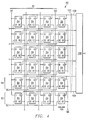
- Figure 4 is a schematic view of a typical memory plane 80 similar to the memory planes 60, 62, 64, and 66 shown in Figure 3.
- Memory plane 80 holds a 4-bit word for each of six pixels in a row.
- the data word for the first pixel is written into the first row 82 of four memory cells 84 in the memory plane 80 through the input data bus 86, the least significant bit on signal 88 and the most significant bit on signal 90.
- the memory write cycle for memory cells 84 is enabled by row enable signal 92.
- Data for the second pixel is loaded into the second row 94 of memory cells using row enable signal 96.
- the third through the sixth image data words are then written into the memory plane 80, filling all of the memory cells 84 in the memory plane 80.
- Data is read out of the array of memory cells 84 one column at a time.
- column output enable signal 98 enables memory cell column 100 to drive the data output bus 102.
- Memory cell column 100 drives the least significant bit of the data word for pixel 1 onto line 104 and the least significant bit of the data word for pixel 6 onto line 106.
- the image data output by the reformatter 80 may be stored in a frame memory until it is necessary to display the data.
- Prior art data reformatters have performed a parallel to serial conversion on the reformatted data in order to avoid an excessive number of interconnections between the data reformatter and the frame memory.
- the parallel to serial conversion was typically performed by an array of parallel-input shift registers on the output of the data reformatter.
- the present invention envisions combining a data reformatter 59 and a frame memory in a single integrated circuit, eliminating the need for the array of shift registers.
- Figure 5 is a block diagram of reformatter/frame memory 112 according to the present invention.
- Data representing one row of pixels is input via input bus 114 into one half of the reformatter 61.
- the positions of switches 68 and 70 are changed to allow the next row of data to be written into second half of the reformatter 63 while the first row of reformatted data is being read from the first half of the reformatter 61 and into the frame memory 122 where it is stored until required for display.
- the interface between the frame memory 122 and the digital display device 124 includes two shift register arrays to reduce the number of interconnections.
- the first shift register array 126 is fabricated on the reformatter/frame memory 112 integrated circuit and, according to one embodiment of the present invention, is comprised of 27 32-bit parallel-input serial-output shift registers. Data for one row of the display is loaded into the first shift register array 126 and shifted out in the form of 32 27-bit words. Each of the 27-bit data words is comprised of one bit from every 32nd pixel in the row.
- the digital display device 124 includes a second array of input shift registers that receive the 32 27-bit data words and perform a serial to parallel conversion on the data to recreate the 864-bit-wide data word.
- the controller 132 shown in Figure 5 supplies the address data, timing signals, and switch control signals to the reformatter/frame memory 112 and the display device 124 which are necessary to coordinate the transfer of data through the reformatter/frame memory 112 to the display device 124.
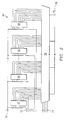
- FIGs 6, 7, 8, and 9 are block diagrams showing a reformatter/frame memory and digital display device in four different digital television systems.
- Figure 6 illustrates the use of two reformatter/frame memories 134, each of which stores data for one-half row of pixels.
- Each reformatter/frame memory 134 includes an array of 27 16-bit shift registers which allow one row of pixel data to be read from the frame memories in 16 words.
- the display system in Figure 7 alternates between two reformatter/frame memories 144 in a ping-pong fashion.
- each reformatter/frame memory 144 store an entire frame and are used to output one frame while the other reformatter/frame memory 144 is being written to.
- dimensions of the reformatter/frame memory are the same as discussed above for Figure 5.
- FIG 8 shows the use of four reformatter/frame memories 140 to reformat and store one frame of video data.
- each reformatter/frame memory 140 stores one-fourth of each line of the video data.
- Each quarter line of data is transferred between a reformatter/frame memory 140 and the digital display device 142 in 16 32-bit words.
- the digital display device 142 receives the 32-bit words in parallel and converts them into one 2048-bit word using the shift register technique discussed above.
- the reformatter/frame memories 140 separately reformat the left, left center, right center, and right quarters of each row.
- Figure 9 shows the use of two separate data paths onto the digital display device 146.
- One data reformatter/frame memory 148 loads data into half of the digital display device, in this example lines 1 through 240, using a first data path 150.
- the second data reformatter/frame memory 154 loads data into the other half of the digital display device, lines 241 through 480, using data path 156.
- the display device may be a digital display, it should be understood that the digital image data may be converted to analog image data and displayed on an analog display device.
Landscapes
- Engineering & Computer Science (AREA)
- Multimedia (AREA)
- Signal Processing (AREA)
- Physics & Mathematics (AREA)
- General Physics & Mathematics (AREA)
- Theoretical Computer Science (AREA)
- Computer Hardware Design (AREA)
- Optics & Photonics (AREA)
- General Engineering & Computer Science (AREA)
- Controls And Circuits For Display Device (AREA)
Applications Claiming Priority (4)
| Application Number | Priority Date | Filing Date | Title |
|---|---|---|---|
| US33254594A | 1994-10-31 | 1994-10-31 | |
| US332545 | 1994-10-31 | ||
| US08/333,199 US5680156A (en) | 1994-11-02 | 1994-11-02 | Memory architecture for reformatting and storing display data in standard TV and HDTV systems |
| US333199 | 1994-11-02 |
Publications (2)
| Publication Number | Publication Date |
|---|---|
| EP0709822A2 true EP0709822A2 (de) | 1996-05-01 |
| EP0709822A3 EP0709822A3 (de) | 1996-07-31 |
Family
ID=26988267
Family Applications (1)
| Application Number | Title | Priority Date | Filing Date |
|---|---|---|---|
| EP95117187A Withdrawn EP0709822A3 (de) | 1994-10-31 | 1995-10-31 | Verbesserungen an oder im Zusammenhang mit Datenformatiereinrichtungen und Bildspeichern |
Country Status (1)
| Country | Link |
|---|---|
| EP (1) | EP0709822A3 (de) |
Cited By (2)
| Publication number | Priority date | Publication date | Assignee | Title |
|---|---|---|---|---|
| WO1999026225A1 (en) * | 1997-11-14 | 1999-05-27 | S-Vision, Inc. | System and method for data planarization |
| EP0827129A3 (de) * | 1996-08-30 | 1999-08-11 | Texas Instruments Incorporated | Formatierung und Speicherung von Daten für Anzeigesysteme mit einem räumlichen Lichtmodulator |
Citations (1)
| Publication number | Priority date | Publication date | Assignee | Title |
|---|---|---|---|---|
| US5278562A (en) | 1992-08-07 | 1994-01-11 | Hughes Missile Systems Company | Method and apparatus using photoresistive materials as switchable EMI barriers and shielding |
Family Cites Families (4)
| Publication number | Priority date | Publication date | Assignee | Title |
|---|---|---|---|---|
| CA2063744C (en) * | 1991-04-01 | 2002-10-08 | Paul M. Urbanus | Digital micromirror device architecture and timing for use in a pulse-width modulated display system |
| US5255100A (en) * | 1991-09-06 | 1993-10-19 | Texas Instruments Incorporated | Data formatter with orthogonal input/output and spatial reordering |
| US5285407A (en) * | 1991-12-31 | 1994-02-08 | Texas Instruments Incorporated | Memory circuit for spatial light modulator |
| DE69411859T2 (de) * | 1993-11-30 | 1999-02-11 | Texas Instruments Inc | Digitaler Speicher für ein Anzeigesystem mit räumlichem Lichtmodulator |
-
1995
- 1995-10-31 EP EP95117187A patent/EP0709822A3/de not_active Withdrawn
Patent Citations (1)
| Publication number | Priority date | Publication date | Assignee | Title |
|---|---|---|---|---|
| US5278562A (en) | 1992-08-07 | 1994-01-11 | Hughes Missile Systems Company | Method and apparatus using photoresistive materials as switchable EMI barriers and shielding |
Cited By (2)
| Publication number | Priority date | Publication date | Assignee | Title |
|---|---|---|---|---|
| EP0827129A3 (de) * | 1996-08-30 | 1999-08-11 | Texas Instruments Incorporated | Formatierung und Speicherung von Daten für Anzeigesysteme mit einem räumlichen Lichtmodulator |
| WO1999026225A1 (en) * | 1997-11-14 | 1999-05-27 | S-Vision, Inc. | System and method for data planarization |
Also Published As
| Publication number | Publication date |
|---|---|
| EP0709822A3 (de) | 1996-07-31 |
Similar Documents
| Publication | Publication Date | Title |
|---|---|---|
| US5680156A (en) | Memory architecture for reformatting and storing display data in standard TV and HDTV systems | |
| KR100266148B1 (ko) | 공간 광 변조기용 프레임 버퍼를 포함하는 그래픽 영상 디스플레이 시스템 및 그 동작방법 | |
| EP0098868B1 (de) | Vorrichtung zur Steuerung eines Farbbildschirmes | |
| EP0530759B1 (de) | Datenformatiereinrichtung mit orthogonaler Eingabe/Ausgabe und räumlicher Neuordnung | |
| US5469190A (en) | Apparatus for converting twenty-four bit color to fifteen bit color in a computer output display system | |
| US5254980A (en) | DMD display system controller | |
| US4751446A (en) | Lookup table initialization | |
| US5606347A (en) | Devices systems and methods for flexible format data storage | |
| US5473342A (en) | Method and apparatus for on-the-fly multiple display mode switching in high-resolution bitmapped graphics system | |
| US5854620A (en) | Method and apparatus for converting monochrome pixel data to color pixel data | |
| EP0360243B1 (de) | Videospeicheranordnung | |
| JPH0690613B2 (ja) | 表示制御装置 | |
| US5086295A (en) | Apparatus for increasing color and spatial resolutions of a raster graphics system | |
| US5414447A (en) | Frame buffer, method and circuit | |
| EP0709822A2 (de) | Verbesserungen an oder im Zusammenhang mit Datenformatiereinrichtungen und Bildspeichern | |
| CN1056929C (zh) | 使用空间光调制器的显示系统的数字存储器 | |
| JP2849075B2 (ja) | 表示フォーマット変換器 | |
| US5309552A (en) | Programmable multi-format display controller | |
| EP0264603B1 (de) | Digitales nach dem Rasterverfahren arbeitendes Anzeigesystem | |
| JPH09149380A (ja) | 標準tvシステムおよびhdtvシステムの表示データをリフォーマットして記憶するメモリ構造体 | |
| EP0513451B1 (de) | Speicheranordnung | |
| US4901062A (en) | Raster scan digital display system | |
| JPH071425B2 (ja) | ラスタ走査表示システム | |
| JPH06102842A (ja) | 分割シリアルレジスタ及び動作カウンタの付いたビデオランダムアクセスメモリを含むグラフィックディスプレイシステム | |
| JP3234046B2 (ja) | カラーグラフィックス装置 |
Legal Events
| Date | Code | Title | Description |
|---|---|---|---|
| PUAI | Public reference made under article 153(3) epc to a published international application that has entered the european phase |
Free format text: ORIGINAL CODE: 0009012 |
|
| AK | Designated contracting states |
Kind code of ref document: A2 Designated state(s): DE FR GB IT NL |
|
| PUAL | Search report despatched |
Free format text: ORIGINAL CODE: 0009013 |
|
| AK | Designated contracting states |
Kind code of ref document: A3 Designated state(s): DE FR GB IT NL |
|
| 17P | Request for examination filed |
Effective date: 19970129 |
|
| 17Q | First examination report despatched |
Effective date: 20020204 |
|
| GRAH | Despatch of communication of intention to grant a patent |
Free format text: ORIGINAL CODE: EPIDOS IGRA |
|
| STAA | Information on the status of an ep patent application or granted ep patent |
Free format text: STATUS: THE APPLICATION IS DEEMED TO BE WITHDRAWN |
|
| 18D | Application deemed to be withdrawn |
Effective date: 20030227 |