EP0709868B1 - Disjoncteur - Google Patents
Disjoncteur Download PDFInfo
- Publication number
- EP0709868B1 EP0709868B1 EP94119681A EP94119681A EP0709868B1 EP 0709868 B1 EP0709868 B1 EP 0709868B1 EP 94119681 A EP94119681 A EP 94119681A EP 94119681 A EP94119681 A EP 94119681A EP 0709868 B1 EP0709868 B1 EP 0709868B1
- Authority
- EP
- European Patent Office
- Prior art keywords
- plate
- movable
- movable member
- contact
- shaped portion
- Prior art date
- Legal status (The legal status is an assumption and is not a legal conclusion. Google has not performed a legal analysis and makes no representation as to the accuracy of the status listed.)
- Expired - Lifetime
Links
Images


Classifications
-
- H—ELECTRICITY
- H01—ELECTRIC ELEMENTS
- H01H—ELECTRIC SWITCHES; RELAYS; SELECTORS; EMERGENCY PROTECTIVE DEVICES
- H01H73/00—Protective overload circuit-breaking switches in which excess current opens the contacts by automatic release of mechanical energy stored by previous operation of a hand reset mechanism
- H01H73/02—Details
- H01H73/04—Contacts
-
- H—ELECTRICITY
- H01—ELECTRIC ELEMENTS
- H01H—ELECTRIC SWITCHES; RELAYS; SELECTORS; EMERGENCY PROTECTIVE DEVICES
- H01H83/00—Protective switches, e.g. circuit-breaking switches, or protective relays operated by abnormal electrical conditions otherwise than solely by excess current
Definitions
- This invention relates to a molded-case circuit breaker, and more particularly to an improvement of the movable member in the circuit breaker which is operated to open and close the circuit.
- FIGS. 8 through 10 shows a conventional circuit breaker disclosed by, for instance, Japanese Utility Patent Publication No. 32922/1993.
- FIG. 8 is a side view of the circuit breaker which is tripped
- FIG. 9 is a side view of the latter which is in "on" state (the circuit being closed).
- reference numeral 1 designates a casing of synthetic resin comprising a cover 1a and a base 1b; 2, a stationary member provided on the bottom of the base 1b, the stationary member 2 having a stationary contact 2a; 3, a frame secured to the base 1b of the casing 1 with screws 4; 5, an operating handle which is swingable about a protrusion 3a formed on the frame 3; 6, a cradle rotatably mounted on the operating handle 5; 7, an upper link pin; and 8, a link mechanism comprising an upper link 8a and a lower link 8b which are coupled to each other through a coupling pin 9. Further in FIGS.
- reference numeral 10 designates a pulling spring which urges the coupling pin 9 towards the operating handle 5 to lock the upper link 8a to the upper link pin 7; 11, a cross bar which is rotatably provided with respect to the base 1b, the cross bar being coupled to the lower link 8b through a lower link pin 12; and 13, a movable member having a movable contact 13a, the movable member 13 being rotatably mounted on a movable member shaft 14 embedded in the cross bar 11.
- reference numeral 15 denotes a stationary conductor secured to the base 1b; 16, a flexible conductor connected between the stationary conductor 15 and the movable member 13; 17, an instantaneous tripping electromagnetic device mounted on the base 1b, having a movable iron core 17a; 18, a timed tripping bimetal device; 18a, an adjusting screw for adjusting the tripping operation; 19, a trip bar which is engaged with the movable iron core 17a and the adjusting screw 18a; 20, a hook which is engaged with the trip bar 19; and 21, a latch adapted to engage with the hook 20, with the cradle 6 being engaged with the latch 21.
- FIG. 9 reference numeral 15 denotes a stationary conductor secured to the base 1b; 16, a flexible conductor connected between the stationary conductor 15 and the movable member 13; 17, an instantaneous tripping electromagnetic device mounted on the base 1b, having a movable iron core 17a; 18, a timed tripping bimetal device; 18a, an
- reference numeral 22 designates a stopper pin on the frame 3; 23, a link stopper adapted to abut against the stopper pin 22, the link stopper 23 having an abutment portion 23a with which the upper link 8a is elastically brought into contact when tripped; and 24, a conventional de-ionization arc extinguish chamber.
- FIG. 10 shows an example of the movable member which is made up of a flat-plate-shaped movable conductor 13b, and a movable contact 13a blazed to one surface of the conductor 13b which corresponds to the thickness of the latter 13b.
- FIG. 11 shows a movable member 13 disclosed by Japanese Utility Patent Application (OPI) No. 41348/1990 (the term "OPI" as used herein means an "unexamined application”), which is coupled to the base 1b.
- OPI Japanese Utility Patent Application
- the movable member 13 is also made up of a flat-plate-shaped movable conductor 13b, and a movable contact 13a which is blazed to one surface of the movable conductor 13b which corresponds to the width of the latter 13b.
- FIG. 12 shows another example of the flat-plate-shaped movable member, which is formed as follows: One end portion of a flat-plate-shaped arm 13b is bent L-shaped to form a flat ear, and a movable contact 13a is blazed to the flat ear thus formed.
- the arm 13b has a hole 14a into which the movable member shaft is inserted.
- FIG. 13 is a plan view outlining the arrangement of a plurality of the movable members 13 shown in FIG.
- the movable member 13 which, as shown in FIG. 10, is formed by blazing the movable contact 13a to the surface of the flat-plate-shaped movable conductor 13b which corresponds to the thickness of the latter 13b, suffers from the following difficulties:
- the flat-plate-shaped movable conductor 13b is reduced in mechanical strength by blazing heat.
- the blazing area of the movable contact 13a is small, so that the movable contact welded to the movable conductor is not sufficiently secured thereto.
- the heat generated in the movable contact 13a by current is not readily conducted to the movable conductor 13a, so that the movable contact 13a is liable to become high in temperature.
- the blazing work is liable to be fluctuated in welding pressure, in welding current, in welding time, and therefore the resultant weld is not stable in mechanical strength. Hence, the blazing work takes time and labor, which increases the manufacturing cost.
- the movable member made up of the flat-plate-shaped movable conductor 13b as shown in FIG. 11 is advantageous as follows: Since the movable conductor 13b is relatively large in width, the movable contact 13a can be blazed to the conductor 13b with ease, or it may be joined to the latter 13b by caulking. In addition, the elasticity of the movable conductor 13b enhances the operation of the latter 13b and that of a link mechanism (not shown).
- the movable member suffers from the following difficulty: Since the slit 1d is large in correspondence to the large width of the movable conductor 13b, arc gas produced at the contact when the circuit is opened is liable to flow through the slit 1d to the tripping device (17 and 18 in FIG. 9).
- the movable member shown in FIG. 12 which comprises; the flat-plate-shaped movable conductor 13b whose one end portion is bent L-shaped to form the flat ear; and movable contact 13a blazed to the flat ear thus formed, is also disadvantageous in the following points:
- the movable contact 13a is liable to be shifted as shown in FIG. 13.
- the centers of the movable contacts 13a are shifted as much as L to the left from the central lines of the flat-plate-shaped conductors 13b, respectively, which are supported on the movable member shaft 14. Accordingly, the center of each of the movable contacts 13a is shifted by L to the left from the center of the casing 1. This shift makes the positional relationship between the stationary contact 2a and the movable contact 13a liable to change, and increases the external dimensions of the circuit breaker depending on its structure.
- an object of this invention is to eliminate the above-described difficulties accompanying a conventional circuit breaker. More specifically, a first object of the invention is to provide a circuit breaker in which its movable member made up of a movable conductor such as a thin metal plate is sufficiently high in mechanical strength, and the movable contact welded to the movable conductor is positively secured to the latter, showing high weld strength, and which is low in manufacturing cost when compared with the conventional one.
- a second object of the invention is to provide a circuit breaker in which arc gas produced at the contact when the circuit is opened scarcely flows to the tripping device (17 and 18 in FIG. 9).
- the movable member may be so modified that it is formed by forging a metal material to include first and second plate-shaped portions which form 90° with each other, and a movable contact is provided on the first plate-shaped portion at the end in such a manner that it is confronted with the stationary contact.
- a portion of the movable conductor which is next to the first plate-shaped portion on which the movable contact is formed may be curved inwardly with respect to the first plate-shaped portion, thus providing a step.
- the movable member may be so modified that it includes: an L-shaped plate material having a protrusion at one end which is bent 90°; and a movable contact provided on the protrusion thus bent in such a manner that the movable contact is confronted with the stationary contact, and the center of the movable contact is on the central line of the movable member.
- the synthetic resin casing may have a partition wall having a slit which is engaged with the portion of the movable conductor 13b which is made perpendicular to the bottom of the casing and is located between the movable contact of the movable member and the cross bar, the slit being made as small in width as permitting the movement of the movable member therein.
- one end portion of the movable conductor made of a metal plate is formed into a first plate-shaped portion having a predetermined width on which the movable contact is provided, and the movable conductor is twisted 90° at the middle so that the remaining portion is perpendicular to the bottom of the casing.
- the movable member thus formed is sufficiently high in mechanism strength, and the movable contact welded to the movable conductor is positively secured to the latter.
- the movable member is so modified that it is formed by forging a metal material and includes the first and second plate-shaped portions which form 90° with each other.
- the movable member thus formed is also sufficiently high in mechanical strength, and the movable contact welded to the movable conductor is positively secured to the latter.
- the portion of the movable conductor which is next to the first plate-shaped portion, on which the movable contact is provided is curved inwardly with respect to the first plate-shaped portion to form the step.
- the step thus formed protects the movable conductor from arc gas produced at the contact.
- the movable member is so modified that it includes: the L-shaped plate material having the protrusion at one end which is bent 90°; and the movable contact provided on the protrusion thus bent in such a manner that the movable contact is confronted with the stationary contact, and the center of the movable contact is on the central line of the movable member.
- the movable member is simple in design and high in mechanical strength, and the movable contact welded to the movable conductor is positively secured to the latter.
- the synthetic resin casing has the partition wall with the slit which is engaged with the portion of the movable conductor which is made perpendicular to the bottom of the casing and is located between the movable contact of the movable member and the cross bar; and the slit is limited in width to the extent that the movable member is movable moved therein.
- the partition wall prevents arc gas produced at the contact from flowing to the tripping device.
- FIG. 1 is a side view, with parts cut away, showing a circuit breaker which is tripped, which constitutes a first embodiment of the invention.
- FIG. 2 is a side view, with parts cut away, showing the circuit breaker which is in "on” state.
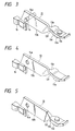
- FIG. 3 is a perspective view of an example of a movable member in the circuit breaker according to the invention.
- FIG. 4 is a perspective view of another example of the movable member in the circuit breaker.
- FIG. 5 is a perspective view showing a movable member in a circuit breaker, which constitutes a second embodiment of the invention.
- FIG. 6(A) is a front view showing a movable member in a circuit breaker, which constitutes a third embodiment of the invention
- FIG. 6(B) is a side view thereof.
- FIG. 7 is a perspective view of a movable member and its relevant component in a circuit breaker, which constitutes a fourth embodiment of the invention.
- FIG. 8 is a side view of a conventional circuit breaker which is tripped.
- FIG. 9 is a side views of the conventional circuit breaker which is in "on" state.
- FIGS. 10 through 12 are perspective views showing examples of a movable member in the conventional circuit breaker.
- FIG. 13 is an explanatory diagram showing a plurality of the movable members shown in FIG. 12 which are applied to a multi-pole circuit breaker.
- FIGS. 1 and 2 show a circuit breaker with a part of its molded casing cut away, which constitutes a first embodiment of the invention. More specifically, FIG. 1 is a side view of the circuit breaker which is tripped, and FIG. 2 is a side view of the latter which is in "on" state (the circuit being closed).
- the components except a base 1b and a movable member 13 are equal to those in the above-described conventional circuit breaker, and are therefore designated by the same reference numerals or characters in FIGS. 1 and 2.
- parts corresponding functionally to those in the conventional circuit breaker are designated by the same reference numerals or characters.
- FIG. 3 shows an example of the movable member 13 in the first embodiment of the invention.
- reference character 13b designates a movable conductor fabricated from a conductive metal plate such as a copper plate or brass plate.
- the movable conductor 13b has a movable contact 13a on its one end portion.
- the one end portion of the movable conductor 13b is formed into a plate-shaped portion 13d larger in width than the diameter of the movable contact 13a.
- a movable contact mounting hole 13c is formed in the plate-shaped portion 13d, so that the movable contact 13a is fixedly secured to the plate-shaped portion 13d by caulking.
- reference numeral 14 denotes a movable member shaft; and 14a, a rotary shaft hole into which the movable member shaft 14 is inserted.
- the movable member 13 thus formed is rotatably held through the movable member shaft 14 on the cross bar 11 (shown in FIG. 1).
- the portion of the movable conductor 13b which is next to the plate-shaped portion 13d is curved inwardly with respect to the latter 13d, to form a step 13f.
- the movable contact 13a is fixedly secured to the movable conductor 13b; however, the invention is not limited thereto or thereby. For instance, as shown in FIG. 4, a round or square movable contact may be secured to it by blazing.
- the movable conductor 13b is made of a metal plate. However, as shown in FIG. 5, it may be formed by forging copper material or brass material. That is, in the second embodiment, the movable conductor 13b is formed by cold forging so that it comprises: a plate-shaped portion 13d at one end which has a predetermined width in correspondence to the size of the movable contact 13a; and the remaining portion which is also in the form of a plate which has a thickness smaller than the predetermined width of the plate-shaped portion 13d. The remaining portion is oriented at 90° with respect to the plate-shaped portion 13d so that it is perpendicular to the bottom of the base 1b.
- the movable conductor 13b is made of a metal plate. However, as shown in FIG. 5, it may be formed by forging copper material or brass material. That is, in the second embodiment, the movable conductor 13b is formed by cold forging so that it comprises: a plate-shaped portion 13d at one end which has a predetermined width in correspondence to the
- reference character 13f designates a step; and 14a, a rotary shaft hole.
- the movable member whose movable conductor 13b is formed by forging in the above-described manner has the same effects as the movable member made of a metal plate in the first embodiment.
- the middle portion of the movable conductor 13b is twisted through 90° so that one end portion of the movable conductor 13b is provided as the plate-shaped portion on which the movable contact 13a is formed, and the remaining portion is perpendicular to the bottom of the base 1b.
- a movable member formed as shown in FIG. 6 may be employed with the same effects. That is, in the third embodiment, the movable member 13 is formed by bending a plate material.
- FIGS. 6(A) and 6(B) are a plan view and a side view of the movable member 13, respectively. As shown in FIGS.
- a movable conductor 13b for forming the movable member 13 is made of an L-shaped plate whose one end portion is formed into a plate-shaped portion 13d having a predetermined width, on which a movable contact 13a is formed.
- the plate-shaped portion 13d is bent through 90° so that the remaining portion is perpendicular to the bottom of the base 1b.
- the middle portion of the movable conductor 13b is so bent that the center of the movable contact 13a is on the central line of the movable member 13.
- the casing 1 has a partition wall with a slit.
- the slit is engaged with the portion of the movable conductor 13b which is made perpendicular to the bottom of the base 1b and is located between the movable contact 13a of the movable member 13 and the cross bar 11.
- the partition wall is as indicated at 1e in FIG. 7.
- the partition wall 1e has the slit 1d which is made as small in width as permitting the movement of the movable member 13 (in the directions of the arrow A) in the slit.
- the partition wall 1e prevents the arc gas g produced at the contact from flowing to the tripping device (17 and 18 in FIG. 9).
- the circuit breaker which is designed as described above, has the following effects or merits:
- one end portion of the movable conductor made is formed into the first plate-shaped portion having the predetermined width on which the movable contact is provided, and the movable conductor is twisted 90° at the middle so that the other end portion is perpendicular to the bottom of the casing.
- This structure increases the mechanical strength of the supporting portion of the movable member during switching, and enhances the welding of the movable contact.
- the movable contact welded to the movable conductor is positively secured to the latter, and the movable member can be pivotally supported with ease.
- the movable member is formed by forging a metal material to include the first and second plate-shaped portions which form 90° with each other.
- the movable member thus formed is also sufficiently high in mechanical strength, and the movable contact welded to the movable conductor is positively secured to the latter.
- the movable conductor has the portion which is next to the first plate-shaped portion on which the movable contact is provided, and is curved inwardly with respect to the first plate-shaped portion to form the step.
- the step thus formed protects the movable conductor from the arc gas produced at the contact.
- the movable member is made up of the L-shaped plate material having the protrusion at one end which is bent 90°.
- the movable member thus formed is simple in in design, and high in mechanical strength, and the movable contact welded to the movable conductor is positively secured to the latter.
- the synthetic resin casing has the partition wall with the slit which is engaged with the portion of the movable conductor which is made perpendicular to the bottom of the casing and is located between the movable contact of the movable member and the cross bar, and the slit is limited in width to the extent that the movable member is movable therein.
- the partition wall prevents the arc gas produced at the contact from flowing to the tripping device.
Landscapes
- Breakers (AREA)
Claims (9)
- Disjoncteur de circuit, comprenant :un élément fixe (2) ayant un contact fixe (2a) à une portion d'extrémité de celui-ci, ledit élément fixe (2) étant prévu sur le côté du fond (1b) d'un boítier (1) en résine synthétique;un élément mobile (13) comprenant une première et une seconde portions en forme de plaque (13d, 13b) qui sont formées soit en tordant la portion milieu (13e) d'une plaque métallique soit en forgeant un matériau métallique de sorte que lesdites portions en forme de plaque (13d, 13b) sont agencées en un angle de 90° l'une à l'autre, ladite première portion en forme de plaque (13d) ayant un contact mobile (13a) qui est fixé à son extrémité par matage d'une manière telle que ledit contact mobile (13a) soit opposé audit contact fixe (2a), les première et seconde portions en forme de plaque (13d, 13b) sont formées d'une manière telle que le centre dudit contact mobile (13a) soit sur la ligne centrale dudit élément mobile (13); etune barre transversale (11) qui supporte l'extrémité de ladite seconde portion en forme de plaque (13b) et est couplée à un mécanisme de commutation (8), et qui est adaptée pour actionner ledit élément mobile (13) de sorte que ledit contact mobile (13a) soit déplacé en engagement et hors d'engagement avec ledit contact fixe (2a).
- Disjoncteur de circuit selon la revendication 1, caractérisé en ce que l'élément mobile précité (13) a une portion qui est proche de la première portion en forme de plaque précitée (13d) sur laquelle est formé le contact mobile précité (13a), et est courbé à l'intérieur par rapport à ladite première portion en forme de plaque (13d), réalisant ainsi un palier (13f).
- Disjoncteur de circuit, comprenant :un élément fixe (2) ayant un contact fixe (2a) sur une portion d'extrémité de celui-ci, ledit élément fixe (2) étant prévu sur le côté du fond (1b) d'un boítier (1) en résine synthétique;un élément mobile (13) comprenant un matériau en plaque en forme de L ayant une saillie à une extrémité qui est recourbée de 90°, un contact mobile (13a) étant prévu sur ladite saillie par matage, le matériau en plaque étant recourbé d'une manière telle que ledit contact mobile (13a) soit opposé audit contact fixe (2a) et le centre dudit contact mobile (13a) soit sur la ligne centrale dudit élément mobile (13); etune barre transversale (11) qui supporte l'extrémité de ladite seconde portion en forme de plaque (13b) et est couplée à un mécanisme de commutation (8), qui est adapté pour actionner ledit élément mobile (13) de sorte que ledit contact mobile (13a) soit déplacé en engagement et hors d'engagement avec le et du contact fixe (2a).
- Disjoncteur de circuit selon l'une des revendications précédentes, caractérisé en ce que le boítier (1) précité en résine synthétique a une paroi de séparation (le) ayant une fente (1d) qui est engagée avec la portion de l'élément mobile précité (13) qui est rendue perpendiculaire au fond dudit boítier (1) et est située entre le contact mobile précité (13a) dudit élément mobile (13) et la barre transversale précitée (11), la largeur de ladite fente (1d) étant choisie de façon que ledit élément mobile (13) puisse se déplacer dans celle-ci.
- Elément mobile (13) adapté pour être installé dans un disjoncteur de circuit pour ouvrir et fermer un circuit en coopération avec un élément fixe (2) ayant un contact fixe (2a), ledit élément mobile (13) comprenant :une première portion en forme de plaque (13d) sur laquelle un contact mobile (13a) est prévu; etune seconde portion en forme de plaque (13b) orientée à 90° par rapport à ladite première portion en forme de plaque (13d), ladite seconde portion en forme de plaque (13b) définissant une ligne centrale;où lesdites première et seconde portions en forme de plaque (13d, 13b) sont intégralement reliées l'une à l'autre d'une manière telle qu'un centre dudit contact mobile (13a) soit sensiblement situé sur ladite ligne centrale; etoù ledit contact mobile (13a) est fixé à l'extrémité de ladite première portion en forme de plaque (13d) par matage.
- Elément mobile selon la revendication 5, caractérisé en ce que ledit élément mobile (13) est formé en torsadant la portion milieu (13e) d'une plaque métallique, laquelle portion est située entre les première et seconde portions en forme de plaque précitées (13d, 13b).
- Elément mobile selon la revendication 5, caractérisé en ce que ledit élément mobile (13) est formé en forgeant un matériau métallique.
- Elément mobile selon la revendication 5, caractérisé en ce que la seconde portion en forme de plaque précitée (13d) comprend une première section définissant la ligne centrale précitée, une seconde section parallèle à ladite première section et déplacée de ladite ligne centrale et une troisième section reliant intégralement ladite première section à ladite seconde section, où la première portion en forme de plaque précitée (13b) est reliée intégralement à ladite seconde section.
- Elément mobile selon la revendication 8, caractérisé en ce que ledit élément mobile (13) est formé à partir d'une plaque métallique en forme de L.
Applications Claiming Priority (3)
| Application Number | Priority Date | Filing Date | Title |
|---|---|---|---|
| JP205117/94 | 1994-08-30 | ||
| JP20511794 | 1994-08-30 | ||
| JP20511794A JP3230197B2 (ja) | 1994-08-30 | 1994-08-30 | 回路遮断器 |
Publications (3)
| Publication Number | Publication Date |
|---|---|
| EP0709868A1 EP0709868A1 (fr) | 1996-05-01 |
| EP0709868B1 true EP0709868B1 (fr) | 1998-04-08 |
| EP0709868B2 EP0709868B2 (fr) | 2002-10-16 |
Family
ID=16501709
Family Applications (1)
| Application Number | Title | Priority Date | Filing Date |
|---|---|---|---|
| EP94119681A Expired - Lifetime EP0709868B2 (fr) | 1994-08-30 | 1994-12-13 | Disjoncteur |
Country Status (7)
| Country | Link |
|---|---|
| EP (1) | EP0709868B2 (fr) |
| JP (1) | JP3230197B2 (fr) |
| KR (1) | KR0170540B1 (fr) |
| CN (1) | CN1039858C (fr) |
| DE (1) | DE69409526T3 (fr) |
| SG (1) | SG48879A1 (fr) |
| TW (1) | TW288148B (fr) |
Families Citing this family (2)
| Publication number | Priority date | Publication date | Assignee | Title |
|---|---|---|---|---|
| JP6124930B2 (ja) * | 2014-05-02 | 2017-05-10 | 日新製鋼株式会社 | マルテンサイト系ステンレス鋼板およびメタルガスケット |
| CN120572152B (zh) * | 2025-08-05 | 2025-10-03 | 四川电器集团中低压智能配电有限公司 | 一种开关设备用连续性焊接装置及其焊接方法 |
Family Cites Families (17)
| Publication number | Priority date | Publication date | Assignee | Title |
|---|---|---|---|---|
| GB207363A (en) * | 1922-11-07 | 1923-11-29 | William Preston | Improvements in or relating to electric switches |
| DE1138139B (de) * | 1960-05-13 | 1962-10-18 | Licentia Gmbh | Aus Flachmaterial bestehende Kontaktanordnung |
| GB926076A (en) * | 1960-08-25 | 1963-05-15 | Bryant Electric Co | Electric circuit breakers |
| US3311729A (en) † | 1965-10-04 | 1967-03-28 | Deringer Mfg Company | Electrical contact and method of forming the same |
| US3329913A (en) † | 1966-01-28 | 1967-07-04 | Heinemann Electric Co | Circuit breaker mechanism |
| US3464040A (en) | 1967-09-21 | 1969-08-26 | Gen Electric | Compact circuit breaker construction |
| US3564184A (en) * | 1969-01-27 | 1971-02-16 | Gen Electric | Electric circuit breaker |
| US3562467A (en) † | 1969-06-04 | 1971-02-09 | Engelhard Min & Chem | Electrical contact |
| DE2525810C3 (de) † | 1975-06-06 | 1986-02-13 | Licentia Patent-Verwaltungs-Gmbh, 6000 Frankfurt | Gleich- und Wechselspannung schaltendes Luftschütz höherer Schaltleistung mit permanentmagnetischem Lichtbogenblassystem |
| JPS53144446A (en) † | 1977-05-24 | 1978-12-15 | Kurata Denshi Kk | Stamping of l or t shaped element with cylindrical handle and said element produced by said stamping |
| JPS54150678A (en) † | 1978-05-19 | 1979-11-27 | Tetsuo Takano | Square electric contact |
| FR2541520B1 (fr) † | 1983-02-21 | 1985-07-19 | Merlin Gerin | Piece de contact electrique et son procede de fabrication |
| JPH0532922Y2 (fr) | 1986-09-09 | 1993-08-23 | ||
| US5286934A (en) † | 1991-09-23 | 1994-02-15 | General Electric Company | Molded case circuit breaker movable contact arm arrangement |
| JPH05101764A (ja) † | 1991-10-08 | 1993-04-23 | Toshiba Corp | 回路遮断器の可動接触子の製造方法 |
| US5302787A (en) * | 1992-05-05 | 1994-04-12 | Square D Company | Automatic miniature circuit breaker with Z-axis assemblable contact assembly |
| JP3116546U (ja) | 2005-09-09 | 2005-12-08 | 株式会社青山 | 装飾用リボン |
-
1994
- 1994-08-30 JP JP20511794A patent/JP3230197B2/ja not_active Ceased
- 1994-10-04 TW TW083109166A patent/TW288148B/zh not_active IP Right Cessation
- 1994-12-13 EP EP94119681A patent/EP0709868B2/fr not_active Expired - Lifetime
- 1994-12-13 DE DE69409526T patent/DE69409526T3/de not_active Expired - Lifetime
- 1994-12-13 SG SG1996003327A patent/SG48879A1/en unknown
-
1995
- 1995-08-28 CN CN95116937A patent/CN1039858C/zh not_active Expired - Fee Related
- 1995-08-28 KR KR1019950026795A patent/KR0170540B1/ko not_active Expired - Fee Related
Also Published As
| Publication number | Publication date |
|---|---|
| KR0170540B1 (ko) | 1999-03-30 |
| JP3230197B2 (ja) | 2001-11-19 |
| HK1010073A1 (en) | 1999-06-11 |
| DE69409526T3 (de) | 2003-06-12 |
| EP0709868B2 (fr) | 2002-10-16 |
| DE69409526D1 (de) | 1998-05-14 |
| JPH0869740A (ja) | 1996-03-12 |
| TW288148B (fr) | 1996-10-11 |
| CN1123457A (zh) | 1996-05-29 |
| CN1039858C (zh) | 1998-09-16 |
| DE69409526T2 (de) | 1998-08-06 |
| EP0709868A1 (fr) | 1996-05-01 |
| KR960008890A (ko) | 1996-03-22 |
| SG48879A1 (en) | 1998-05-18 |
Similar Documents
| Publication | Publication Date | Title |
|---|---|---|
| EP0593688B1 (fr) | Disjoncteur miniature automatique avec mecanisme de declenchement a assemblage dans l'axe des z | |
| US5302787A (en) | Automatic miniature circuit breaker with Z-axis assemblable contact assembly | |
| US5250918A (en) | Automatic miniature circuit breaker with Z-axis assemblage current response mechanism | |
| AU2002214177B2 (en) | Circuit interrupter with thermal trip adjustability | |
| US6107902A (en) | Circuit breaker with visible trip indicator | |
| AU2002214177A1 (en) | Circuit interrupter with thermal trip adjustability | |
| US4080582A (en) | Circuit breaker with improved trip mechanism | |
| US6407653B1 (en) | Circuit interrupter with a magnetically-induced automatic trip assembly having adjustable armature biasing | |
| EP0709868B1 (fr) | Disjoncteur | |
| US6633211B1 (en) | Circuit interrupter with a magnetically-induced automatic trip assembly having improved armature pivoting | |
| EP0752155A1 (fr) | Ensemble a lame | |
| US6867672B2 (en) | Switching device comprising a latching mechanism | |
| US4047134A (en) | Circuit breaker | |
| HK1010073B (en) | Circuit breaker | |
| EP1126489B1 (fr) | Arbre de déclenchement amélioré pour un disjoncteur avec un espace intérieur réduit | |
| JP3296460B2 (ja) | 回路遮断器 | |
| US7202437B1 (en) | Electrical switching apparatus including operating mechanism having insulating portion | |
| CN111243911A (zh) | 一种新型力学机构断路器 | |
| JPS6340341B2 (fr) | ||
| JPH0423367B2 (fr) | ||
| JPH08148075A (ja) | 接触装置 |
Legal Events
| Date | Code | Title | Description |
|---|---|---|---|
| PUAI | Public reference made under article 153(3) epc to a published international application that has entered the european phase |
Free format text: ORIGINAL CODE: 0009012 |
|
| AK | Designated contracting states |
Kind code of ref document: A1 Designated state(s): DE FR GB NL |
|
| 17P | Request for examination filed |
Effective date: 19960708 |
|
| GRAG | Despatch of communication of intention to grant |
Free format text: ORIGINAL CODE: EPIDOS AGRA |
|
| 17Q | First examination report despatched |
Effective date: 19970908 |
|
| GRAH | Despatch of communication of intention to grant a patent |
Free format text: ORIGINAL CODE: EPIDOS IGRA |
|
| GRAG | Despatch of communication of intention to grant |
Free format text: ORIGINAL CODE: EPIDOS AGRA |
|
| GRAH | Despatch of communication of intention to grant a patent |
Free format text: ORIGINAL CODE: EPIDOS IGRA |
|
| GRAA | (expected) grant |
Free format text: ORIGINAL CODE: 0009210 |
|
| AK | Designated contracting states |
Kind code of ref document: B1 Designated state(s): DE FR GB NL |
|
| REF | Corresponds to: |
Ref document number: 69409526 Country of ref document: DE Date of ref document: 19980514 |
|
| ET | Fr: translation filed | ||
| PGFP | Annual fee paid to national office [announced via postgrant information from national office to epo] |
Ref country code: NL Payment date: 19981229 Year of fee payment: 5 |
|
| PLBI | Opposition filed |
Free format text: ORIGINAL CODE: 0009260 |
|
| PLBQ | Unpublished change to opponent data |
Free format text: ORIGINAL CODE: EPIDOS OPPO |
|
| PLBF | Reply of patent proprietor to notice(s) of opposition |
Free format text: ORIGINAL CODE: EPIDOS OBSO |
|
| 26 | Opposition filed |
Opponent name: SCHNEIDER ELECTRIC SA Effective date: 19990104 |
|
| NLR1 | Nl: opposition has been filed with the epo |
Opponent name: SCHNEIDER ELECTRIC SA |
|
| REG | Reference to a national code |
Ref country code: GB Ref legal event code: 746 Effective date: 19990519 |
|
| PLBF | Reply of patent proprietor to notice(s) of opposition |
Free format text: ORIGINAL CODE: EPIDOS OBSO |
|
| PLBF | Reply of patent proprietor to notice(s) of opposition |
Free format text: ORIGINAL CODE: EPIDOS OBSO |
|
| REG | Reference to a national code |
Ref country code: FR Ref legal event code: D6 |
|
| PG25 | Lapsed in a contracting state [announced via postgrant information from national office to epo] |
Ref country code: NL Free format text: LAPSE BECAUSE OF NON-PAYMENT OF DUE FEES Effective date: 20000701 |
|
| NLV4 | Nl: lapsed or anulled due to non-payment of the annual fee |
Effective date: 20000701 |
|
| REG | Reference to a national code |
Ref country code: GB Ref legal event code: IF02 |
|
| PLAW | Interlocutory decision in opposition |
Free format text: ORIGINAL CODE: EPIDOS IDOP |
|
| PLAW | Interlocutory decision in opposition |
Free format text: ORIGINAL CODE: EPIDOS IDOP |
|
| PUAH | Patent maintained in amended form |
Free format text: ORIGINAL CODE: 0009272 |
|
| STAA | Information on the status of an ep patent application or granted ep patent |
Free format text: STATUS: PATENT MAINTAINED AS AMENDED |
|
| 27A | Patent maintained in amended form |
Effective date: 20021016 |
|
| AK | Designated contracting states |
Kind code of ref document: B2 Designated state(s): DE FR GB NL |
|
| ET3 | Fr: translation filed ** decision concerning opposition | ||
| PGFP | Annual fee paid to national office [announced via postgrant information from national office to epo] |
Ref country code: GB Payment date: 20031210 Year of fee payment: 10 |
|
| PGFP | Annual fee paid to national office [announced via postgrant information from national office to epo] |
Ref country code: FR Payment date: 20041208 Year of fee payment: 11 |
|
| PG25 | Lapsed in a contracting state [announced via postgrant information from national office to epo] |
Ref country code: GB Free format text: LAPSE BECAUSE OF NON-PAYMENT OF DUE FEES Effective date: 20041213 |
|
| GBPC | Gb: european patent ceased through non-payment of renewal fee |
Effective date: 20041213 |
|
| PG25 | Lapsed in a contracting state [announced via postgrant information from national office to epo] |
Ref country code: FR Free format text: LAPSE BECAUSE OF NON-PAYMENT OF DUE FEES Effective date: 20060831 |
|
| REG | Reference to a national code |
Ref country code: FR Ref legal event code: ST Effective date: 20060831 |
|
| PGFP | Annual fee paid to national office [announced via postgrant information from national office to epo] |
Ref country code: DE Payment date: 20091222 Year of fee payment: 16 |
|
| PG25 | Lapsed in a contracting state [announced via postgrant information from national office to epo] |
Ref country code: DE Free format text: LAPSE BECAUSE OF NON-PAYMENT OF DUE FEES Effective date: 20110701 |
|
| REG | Reference to a national code |
Ref country code: DE Ref legal event code: R119 Ref document number: 69409526 Country of ref document: DE Effective date: 20110701 |