EP0709880A2 - Verfahren zur Bildung von erhöhten Source- und Drainzonen in integrierten Schaltungen - Google Patents
Verfahren zur Bildung von erhöhten Source- und Drainzonen in integrierten Schaltungen Download PDFInfo
- Publication number
- EP0709880A2 EP0709880A2 EP95307656A EP95307656A EP0709880A2 EP 0709880 A2 EP0709880 A2 EP 0709880A2 EP 95307656 A EP95307656 A EP 95307656A EP 95307656 A EP95307656 A EP 95307656A EP 0709880 A2 EP0709880 A2 EP 0709880A2
- Authority
- EP
- European Patent Office
- Prior art keywords
- source
- drain regions
- substrate
- forming
- transistor
- Prior art date
- Legal status (The legal status is an assumption and is not a legal conclusion. Google has not performed a legal analysis and makes no representation as to the accuracy of the status listed.)
- Withdrawn
Links
Images


Classifications
-
- H—ELECTRICITY
- H10—SEMICONDUCTOR DEVICES; ELECTRIC SOLID-STATE DEVICES NOT OTHERWISE PROVIDED FOR
- H10D—INORGANIC ELECTRIC SEMICONDUCTOR DEVICES
- H10D62/00—Semiconductor bodies, or regions thereof, of devices having potential barriers
- H10D62/10—Shapes, relative sizes or dispositions of the regions of the semiconductor bodies; Shapes of the semiconductor bodies
- H10D62/13—Semiconductor regions connected to electrodes carrying current to be rectified, amplified or switched, e.g. source or drain regions
- H10D62/149—Source or drain regions of field-effect devices
- H10D62/151—Source or drain regions of field-effect devices of IGFETs
-
- H—ELECTRICITY
- H10—SEMICONDUCTOR DEVICES; ELECTRIC SOLID-STATE DEVICES NOT OTHERWISE PROVIDED FOR
- H10D—INORGANIC ELECTRIC SEMICONDUCTOR DEVICES
- H10D30/00—Field-effect transistors [FET]
- H10D30/01—Manufacture or treatment
- H10D30/021—Manufacture or treatment of FETs having insulated gates [IGFET]
- H10D30/0223—Manufacture or treatment of FETs having insulated gates [IGFET] having source and drain regions or source and drain extensions self-aligned to sides of the gate
- H10D30/0227—Manufacture or treatment of FETs having insulated gates [IGFET] having source and drain regions or source and drain extensions self-aligned to sides of the gate having both lightly-doped source and drain extensions and source and drain regions self-aligned to the sides of the gate, e.g. lightly-doped drain [LDD] MOSFET or double-diffused drain [DDD] MOSFET
-
- H—ELECTRICITY
- H10—SEMICONDUCTOR DEVICES; ELECTRIC SOLID-STATE DEVICES NOT OTHERWISE PROVIDED FOR
- H10D—INORGANIC ELECTRIC SEMICONDUCTOR DEVICES
- H10D30/00—Field-effect transistors [FET]
- H10D30/01—Manufacture or treatment
- H10D30/021—Manufacture or treatment of FETs having insulated gates [IGFET]
- H10D30/027—Manufacture or treatment of FETs having insulated gates [IGFET] of lateral single-gate IGFETs
- H10D30/0275—Manufacture or treatment of FETs having insulated gates [IGFET] of lateral single-gate IGFETs forming single crystalline semiconductor source or drain regions resulting in recessed gates, e.g. forming raised source or drain regions
-
- H—ELECTRICITY
- H10—SEMICONDUCTOR DEVICES; ELECTRIC SOLID-STATE DEVICES NOT OTHERWISE PROVIDED FOR
- H10D—INORGANIC ELECTRIC SEMICONDUCTOR DEVICES
- H10D30/00—Field-effect transistors [FET]
- H10D30/60—Insulated-gate field-effect transistors [IGFET]
- H10D30/601—Insulated-gate field-effect transistors [IGFET] having lightly-doped drain or source extensions, e.g. LDD IGFETs or DDD IGFETs
-
- H—ELECTRICITY
- H10—SEMICONDUCTOR DEVICES; ELECTRIC SOLID-STATE DEVICES NOT OTHERWISE PROVIDED FOR
- H10D—INORGANIC ELECTRIC SEMICONDUCTOR DEVICES
- H10D62/00—Semiconductor bodies, or regions thereof, of devices having potential barriers
- H10D62/80—Semiconductor bodies, or regions thereof, of devices having potential barriers characterised by the materials
- H10D62/83—Semiconductor bodies, or regions thereof, of devices having potential barriers characterised by the materials being Group IV materials, e.g. B-doped Si or undoped Ge
-
- H—ELECTRICITY
- H10—SEMICONDUCTOR DEVICES; ELECTRIC SOLID-STATE DEVICES NOT OTHERWISE PROVIDED FOR
- H10D—INORGANIC ELECTRIC SEMICONDUCTOR DEVICES
- H10D64/00—Electrodes of devices having potential barriers
- H10D64/01—Manufacture or treatment
- H10D64/011—Manufacture or treatment of electrodes ohmically coupled to a semiconductor
- H10D64/0111—Manufacture or treatment of electrodes ohmically coupled to a semiconductor to Group IV semiconductors
- H10D64/0112—Manufacture or treatment of electrodes ohmically coupled to a semiconductor to Group IV semiconductors using conductive layers comprising silicides
-
- H—ELECTRICITY
- H10—SEMICONDUCTOR DEVICES; ELECTRIC SOLID-STATE DEVICES NOT OTHERWISE PROVIDED FOR
- H10D—INORGANIC ELECTRIC SEMICONDUCTOR DEVICES
- H10D64/00—Electrodes of devices having potential barriers
- H10D64/20—Electrodes characterised by their shapes, relative sizes or dispositions
- H10D64/23—Electrodes carrying the current to be rectified, amplified, oscillated or switched, e.g. sources, drains, anodes or cathodes
- H10D64/251—Source or drain electrodes for field-effect devices
- H10D64/258—Source or drain electrodes for field-effect devices characterised by the relative positions of the source or drain electrodes with respect to the gate electrode
-
- H—ELECTRICITY
- H10—SEMICONDUCTOR DEVICES; ELECTRIC SOLID-STATE DEVICES NOT OTHERWISE PROVIDED FOR
- H10D—INORGANIC ELECTRIC SEMICONDUCTOR DEVICES
- H10D64/00—Electrodes of devices having potential barriers
- H10D64/20—Electrodes characterised by their shapes, relative sizes or dispositions
- H10D64/23—Electrodes carrying the current to be rectified, amplified, oscillated or switched, e.g. sources, drains, anodes or cathodes
- H10D64/251—Source or drain electrodes for field-effect devices
- H10D64/258—Source or drain electrodes for field-effect devices characterised by the relative positions of the source or drain electrodes with respect to the gate electrode
- H10D64/259—Source or drain electrodes being self-aligned with the gate electrode and having bottom surfaces higher than the interface between the channel and the gate dielectric
-
- H—ELECTRICITY
- H10—SEMICONDUCTOR DEVICES; ELECTRIC SOLID-STATE DEVICES NOT OTHERWISE PROVIDED FOR
- H10D—INORGANIC ELECTRIC SEMICONDUCTOR DEVICES
- H10D64/00—Electrodes of devices having potential barriers
- H10D64/60—Electrodes characterised by their materials
- H10D64/62—Electrodes ohmically coupled to a semiconductor
Definitions
- the present invention relates generally to semiconductor integrated circuit processing, and more specifically to an improved method of forming planarized transistors by forming raised source and drain regions while reducing junction leakage and preventing shorting conditions.
- the manufacturing cost of a given integrated circuit is largely dependent upon the chip area required to implement desired functions.
- the chip area is defined by the geometries and sizes of the active components such as gate electrodes in metal-oxide-semiconductor (MOS) technology, and diffused regions such as MOS source and drain regions and bipolar emitters and base regions. These geometries and sizes are often dependent upon the photolithographic resolution available for the particular manufacturing facility.
- the goal of photolithography in establishing the horizontal dimensions of the various devices and circuits is to create a pattern which meets design requirements as well as to correctly align the circuit pattern on the surface of the wafer. As line widths shrink smaller and smaller in submicron photolithography, the process to print lines and contact holes in photoresist becomes increasingly more difficult.
- contact structures as transistor dimensions decrease is also important to predict and control device performance.
- a variety of contact structures have been considered to alleviate various problems such as contact resistance and the maximum area of devices available, such as the areas of source and drain regions, in order to make full contact to the devices with the contact structures.
- Self-aligned silicides are one alternative for alleviating contact area and resistivity problems associated with contacting source and drain regions.
- the self-aligned silicides make the diffused regions more conductive and lowers the sheet resistance of the diffused regions. This self-aligned process is shown with reference to Figures 1 and 2.
- the lightly doped drain (LDD) regions 22 are formed by conventional methods by implanting a light dose at the edge of the gate electrode near the channel to overcome such problems as hot-carrier effects. Sidewall oxide spacers 20 are formed along the edge of the gate electrode and gate oxide.
- the source/drain regions 24 are implanted with a heavier dose to form the source/drain junctions.
- a metal 26 is deposited over the integrated circuit after which the wafer is heated. The silicon in the source/drain regions 24 then reacts with the metal 26 to form a silicide 28 as shown in Figure 2.
- This process is called salicide if the silicide over the source/drain regions is formed at the same time as the silicide 30 over the polysilicon gate electrode. Everywhere there is silicon, the metal will react to form a silicide (the source/drain regions in area 28 and the polysilicon in region 30). Elsewhere the metal remains unreacted and is selectively removed.
- a dielectric layer is typically formed over the integrated circuit with contact openings formed to the source/drain regions and the polysilicon gate. The openings are generally filled with a metal to make contact to the silicide regions 28 and 30.
- the refractory metals including titanium, tungsten, tantalum and cobalt have proven well-suited for use as the metal with which to form the silicide since the reaction with silicon occurs at relatively low processing temperatures, for example, 600° C or less.
- the silicide formation consumes a portion of the substrate silicon thus reducing the integrity of the source/drain regions.
- titanium is commonly used for the silicide metal because of its low resistivity.
- silicon tends to diffuse into the titanium which then may react over top of the sidewall oxide spacers. If silicide is formed over the oxide spacers it is continuous between the silicide formed over the polysilicon gate and the source/drain regions which will cause shorting between the gate electrode and the source/drain regions.
- the invention may be incorporated into a method for forming a semiconductor device structure, and the semiconductor device structure formed thereby.
- a transistor is formed over a substrate having a gate electrode overlying a gate oxide, wherein the transistor is electrically isolated from other devices by a plurality of field oxide regions.
- a dielectric capping layer is formed over the gate electrode.
- LDD regions are formed in the substrate adjacent to the gate electrode.
- Sidewall oxide spacers are formed adjacent to the transistor.
- Raised conductive source/drain regions are formed adjacent to the sidewall oxide spacers and overlying the exposed LDD regions.
- the raised source/drain regions are preferably formed to a height above the substrate which is substantially planar with the height of the transistor above the substrate to aid in the planarization of the wafer before subsequent processing steps occur.
- the raised source/drain regions are preferably formed from selectively grown epitaxial silicon or metal, both of which will aid in reducing punchthrough in the channel under the transistor. If the epitaxial silicon is grown, it is preferable to dope the silicon such that the dopants diffuse into the substrate to form more heavily doped source and drain regions after the epitaxial regions are formed.
- a method of forming a semiconductor integrated circuit comprising the steps of forming a transistor over a substrate having a gate electrode overlying a gate oxide, wherein the transistor is electrically isolated by a plurality of field oxide regions, forming a dielectric capping layer over the gate electrode, forming LDD regions in the substrate adjacent to the gate electrode, forming sidewall oxide spacers adjacent to the transistor, and forming planarizing raised conductive source/drain regions adjacent to the sidewall oxide spacers and overlying substantially all of the LDD regions.
- the capping layer may comprise oxide or nitride.
- the formation of the transistor may comprise the steps of forming an oxide layer over the integrated circuit, forming polysilicon over the gate oxide, and patterning and etching the polysilicon and oxide layers to form the gate electrode and gate oxide, respectively.
- the formation of the transistor may further comprise the step of forming a silicide layer over the polysilicon.
- the height of the transistor above the substrate may be approximately 1000-3500 angstroms.
- the transistor gate electrode may be between approximately .2 to .5 microns wide.
- Forming a planarizing raised conductive source/drain region may further comprise the steps of selectively growing an epitaxial region adjacent to the sidewall oxide spacers over the exposed silicon substrate, and doping the epitaxial region to form conductive raised source/drain regions with sufficient energy and dose to achieve continuity with the LDD implant in the substrate and to form more heavily doped source and drain regions in at least a portion of the LDD regions.
- Forming a planarizing raised conductive source/drain region may additionally comprise the step of siliciding an upper portion of the epitaxial region to reduce the resistivity of the epitaxial region.
- Forming a planarizing raised conductive source/drain region may further comprise the steps of forming more heavily doped substrate source and drain regions in the substrate after the sidewall oxide spacers are formed, forming a metal layer over the integrated circuit to a height greater than the capping layer, patterning and etching the metal layer to remain over the transistor and substrate source and drain regions, and removing the metal layer over the capping layer and a portion of the sidewall oxide spacers.
- the removal of the metal layer may comprise reactive ion etching.
- Forming a planarizing raised conductive source/drain region may further comprise the steps of forming more heavily doped substrate source and drain regions in the substrate after the sidewall oxide spacers are formed, and selectively depositing a metal region over the substrate source and drain regions.
- the height of an upper surface of the planarizing raised source/drain regions above the substrate surface may be approximately the same as the height of an upper surface of the gate electrode of the transistor above the substrate surface.
- the distance between the planarizing raised conductive source/drain regions and the gate electrode may be large enough for adequate electrical isolation to prevent shorting between the raised source/drain regions and the gate electrode.
- Aaccording to another aspect of the present invention there is provided a method of forming a semiconductor integrated circuit, comprising the steps of forming a transistor encapsulated in a dielectric overlying a substrate, forming first source and drain regions in the substrate adjacent the transistor, and forming conductive raised second source and drain regions overlying substantially all of the first substrate source and drain regions and adjacent the transistor, wherein the second source and drain regions are formed such that an upper surface of the raised second source and drain regions are substantially planar with an upper surface of the transistor and wherein the second source and drain regions are electrically isolated from the transistor.
- Forming the conductive raised second source and drain regions step may further comprise the steps of selectively growing an epitaxial region adjacent to the encapsulated transistor over the first substrate source and drain regions, and doping the epitaxial region to form the conductive raised second source and drain regions and to further dope substrate in at least a portion of the first substrate source and drain regions, wherein the first source and drain regions are LDD regions.
- Forming the conductive raised second source and drain regions may further comprise the step of siliciding an upper portion of the epitaxial region to reduce the resistivity of the epitaxial region.
- Forming the conductive raised second source and drain regions step may further comprise the steps of forming heavily doped source and drain regions in the substrate in at least a portion of the first source and drain regions, removing the metal layer over a portion of the encapsulated transistor.
- Forming a planarizing raised conductive source/drain region may further comprise the steps of forming more heavily doped substrate source and drain regions in at least a portion of the first substrate source and drain regions, and selectively depositing a metal layer over the substrate source and drain regions.
- a structure of a portion of a semiconductor integrated circuit formed at a surface of a body comprising a transistor encapsulated in a dielectric overlying a substrate, first source and drain regions in the substrate adjacent the transistor, and conductive raised second source and drain regions overlying substantially all of the first substrate source and drain regions and adjacent the transistor, wherein an upper surface of the raised second source and drain regions is substantially planar with an upper surface of the transistor and wherein the second source and drain regions are electrically isolated from the transistor.
- the conductive raised second source and drain regions may be selectively grown and doped epitaxial silicon.
- the selectively grown and doped epitaxial silicon may further comprise a silicide region at an upper surface of the epitaxial silicon.
- the conductive raised second source and drain regions may be metal.
- the conductive raised second source and drain regions may be selectively deposited metal.
- Figures 1-2 are cross sectional views of the fabrication of a semiconductor integrated circuit according to the prior art.
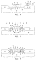
- Figures 3-6 are cross sectional views of the fabrication of a semiconductor integrated circuit according to one embodiment of the present invention.
- Figures 7-8 are cross sectional views of the fabrication of a semiconductor integrated circuit according to a first alternative embodiment of the present invention.
- Figure 9 is a cross sectional view of the fabrication of a semiconductor integrated circuit according to a second alternative embodiment of the present invention.
- Figure 3 illustrates a portion of a wafer, in cross-section, which has a surface at which isolation structures and devices in adjacent active areas are to be formed.
- an integrated circuit is to be formed on a silicon substrate 50.
- the silicon substrate may be p- or n- doped silicon depending upon the location in the wafer where the isolation and active devices are to be formed.
- Field oxide regions 52 are formed on various portions of the wafer to isolate the active areas where devices will be formed.
- a gate oxide layer 54 is thermally grown over the silicon substrate 50 to a depth of approximately 20 to 300 angstroms.
- a polysilicon layer 56 is formed over the oxide layer 54 and field oxide regions 52 to a depth of between approximately 1000-6000 angstroms.
- An dielectric capping layer 58 such as oxide or nitride is then formed over the polysilicon layer 56 to a depth of between approximately 1000 to 2000 angstroms.
- Transistor 60 comprises gate oxide 62, polysilicon gate electrode 64 and dielectric capping layer 66.
- Gate electrode 64 may alternatively comprise a silicide of between approximately 1000 to 2000 angstroms overlying the polysilicon layer. The silicide will help to reduce the sheet resistance of the polysilicon gate.
- Lightly doped drain and source regions 76 are formed, typically with a phosphorous implant in the silicon substrate adjacent to the edge of the gate electrode 64.
- Sidewall oxide spacers 74 are then formed along the edge of the transistor gate. However, with the capping layer 66 overlying the gate electrode 64, the sidewall spacers 74 will also form along the side of the capping layer 66.
- Interconnect 68 is formed over the field oxide region 52 from the same polysilicon layer 56 as that used to form gate electrode 64. After the patterning and etching step, the dielectric capping layer 72 remains over the polysilicon interconnect 70. A silicide may also be formed over the polysilicon underlying the capping layer to reduce the sheet resistance. Sidewall oxide spacers 74 are also formed along the edge of the interconnect 68.
- Regions of epitaxy 80 are selectively grown over the source and drain regions 76.
- epitaxial growth of silicon can be selectively deposited on the exposed silicon substrate without deposition occurring on surrounding regions of oxide.
- the growth of the epitaxial silicon 80 will thus be above the source/drain regions 76.
- the epitaxial regions 80 will form over the source/drain regions 76.
- an upper surface of the epitaxial regions will be formed to a height above the silicon substrate substantially planar with an upper surface of the gate electrode 64.
- Epitaxial regions 80 will be implanted with an N+ or P+ dopant as shown by the arrows in Figure 5.
- the epitaxial regions need to be implanted with sufficient energy and dose to achieve continuity with the LDD implant in the substrate.
- the dopant atoms will diffuse into the silicon in essentially the same shape as the epitaxial regions 80 to form the N+ or P+ source/drain junctions 77 within at least a portion of regions 76.
- the more heavily doped source/drain regions have a deeper junction than the LDD regions as shown by the source/drain regions 24 in Figure 1. While the same depth may be achieved in the present invention, alternatively, the source/drain regions 77 may have the same or less junction depth in the deepest portion than the LDD regions already formed.
- LDD regions may typically form to a depth of approximately 1000 angstroms.
- the dose required for this depth would normally be approximately 1-4 ⁇ 1013 atoms/cm of phosphorous.
- the second more heavily doped source and drain regions junctions are formed to a depth of approximately 1500 angstroms below the silicon surface.
- the implant is typically arsenic at a dose of about 5 ⁇ 1015 atoms/cm. The depth of the source and drain regions can be made deeper than the LDD regions without impacting device performance since the more heavily doped source/drain regions are further away from the channel.
- the silicide formation 28 consumes a portion of the source and drain regions 24, approximately 700 angstroms of the 1500 angstroms. If a large enough amount of silicon is consumed, undesired results may be obtained, for example, there may be a low or leaky drain to substrate diode breakdown voltage and the silicide may encroach into the LDD regions effectively reducing the device integrity.
- the raised source/drain regions 80 formed from selectively growing an epitaxial layer will prevent any lateral diffusion of silicide in the source/drain regions.
- the more heavily doped source/drain regions 77 are formed through the epitaxial regions 80 they can be kept to a depth less than or approximately equal to the depth of the LDD.
- the width of the gate thus the length of the channel "L" may be shortened without adversely affecting device performance.
- the standard submicron gate width is .5 microns, this process may allow reduction of the gate width to between .2 to .4 microns. Reducing the gate width has obvious advantages in submicron processing technology such as increasing switching speeds and allowing for a higher packing density of transistors on the chip.
- a metal layer such as a refractory metal layer, is formed over the integrated circuit.
- the wafer is heated to react the metal with the underlying epitaxial silicon in regions 80 to form a silicide 82.
- Silicide 82 will lower the resistivity of the raised source and drain regions 80.
- the raised source/drain epitaxial regions 80 will prevent any undesired amount of the substrate silicon from being consumed. The possibility of junction leakage and punchthrough are substantially reduced.
- the capping layer 66 and sidewall oxide spacers 74 With the raised source/drain epitaxial regions 80 substantially planar with the upper portion of the gate electrode 64, the capping layer 66 and sidewall oxide spacers 74 will electrically isolate the raised source and drain epitaxial regions 80 from the gate electrode 64 to prevent shorting between the gate and source/drain regions.
- a minimum thickness of the capping layer 66 and sidewall oxide spacers 74 needs to be maintained to provide adequate electrical separation as shown by "D" in Figure 6.
- the raised epitaxial regions with silicide provide for more thermal stability as compared to a conventional salicide process for subsequent high temperature processing steps.
- the N+ or P+ heavily doped source and drain regions 77 are formed by conventional methods after the sidewall oxide spacers are formed and before the raised source/drain regions are formed.
- the junction of the source/drain regions 77 will typically be deeper than the LDD regions 76 as described above with reference to Figures 1 and 2.
- a suitable metal layer for example tungsten, is formed over the integrated circuit, preferably to a height greater than the polysilicon stacks which include the transistor 60 and interconnect 68.
- the metal layer is patterned and etched to form a metal region 86 overlying the transistor 60 and source and drain regions 77.
- a portion of the metal layer 86 is etched away to form raised source/drain regions 88 overlying the source and drain regions 77 and exposing a portion of the capping layer 66 and sidewall oxide spacers 74. Removal of the metal layer may be by any acceptable method of planarization, for example, reactive ion etching selective to the metal chosen.
- the metal is preferably etched until the upper portion of the raised source/drain regions 88 is substantially the same height above the silicon substrate as the upper portion of the gate electrode 64. As with the selectively grown epitaxial raised source/drain regions described above, this will provide for a more planar device for subsequent processing steps.
- the metal raised source/drain regions will eliminate the need for siliciding the source/drain regions 77 in the substrate, thus reducing the possibility of junction leakage and punchthrough.
- the N+ or P+ heavily doped source and drain regions 77 are formed by conventional methods after the sidewall oxide spacers are formed and before the raised source/drain regions are formed.
- the junction of the source/drain regions 77 will typically be deeper than the LDD regions 76.
- Regions of metal 90 are selectively deposited over the source/drain regions 77.
- the metal is preferably a refractory metal, for example, titanium or tungsten. Selective metal deposition may grow a thin layer of metal silicide over the source/drain regions 77 which may consume a portion of the substrate silicon.
- this portion of the selective metal formation acts as a diffusion barrier as the remaining metal continues to be selectively grown over the source/drain regions.
- the metal regions may be deposited to a height substantially planar with the upper surface of the gate 64 of transistor 60, thus reducing the need for an etch back step. While there may be some faceting with the selectively grown epitaxial regions as described above with reference to the preferred embodiment, the selectively deposited metal will form a more planar upper surface. As with each embodiment described, there needs to be a minimum thickness of the capping layer 66 and sidewall oxide spacers 74 to maintain adequate distance between the raised source and drain regions 90 from the gate electrode 64. This distance will insure the necessary electrical isolation of devices and maintain device integrity.
Landscapes
- Insulated Gate Type Field-Effect Transistor (AREA)
- Electrodes Of Semiconductors (AREA)
Priority Applications (1)
| Application Number | Priority Date | Filing Date | Title |
|---|---|---|---|
| EP97200810A EP0785573B1 (de) | 1994-10-31 | 1995-10-27 | Verfahren zur Bildung von erhöhten Source- und Drainzonen in integrierten Schaltungen |
Applications Claiming Priority (2)
| Application Number | Priority Date | Filing Date | Title |
|---|---|---|---|
| US33169194A | 1994-10-31 | 1994-10-31 | |
| US331691 | 1994-10-31 |
Publications (2)
| Publication Number | Publication Date |
|---|---|
| EP0709880A2 true EP0709880A2 (de) | 1996-05-01 |
| EP0709880A3 EP0709880A3 (de) | 1996-10-23 |
Family
ID=23294962
Family Applications (1)
| Application Number | Title | Priority Date | Filing Date |
|---|---|---|---|
| EP95307656A Withdrawn EP0709880A3 (de) | 1994-10-31 | 1995-10-27 | Verfahren zur Bildung von erhöhten Source- und Drainzonen in integrierten Schaltungen |
Country Status (4)
| Country | Link |
|---|---|
| US (1) | US5798278A (de) |
| EP (1) | EP0709880A3 (de) |
| JP (1) | JPH08213616A (de) |
| DE (1) | DE69534688D1 (de) |
Cited By (2)
| Publication number | Priority date | Publication date | Assignee | Title |
|---|---|---|---|---|
| EP0810647A3 (de) * | 1996-05-28 | 1998-07-22 | Harris Corporation | Verfahren zur Herstellung eins MOS-Bauelements mit selbstausgerichteten erhöhten Source- und Drain-Zonen und dadurch hergestelltes Bauelement |
| GB2355583A (en) * | 1999-06-29 | 2001-04-25 | Hyundai Electronics Ind | Method of forming a transistor having elevated source and drain regions |
Families Citing this family (25)
| Publication number | Priority date | Publication date | Assignee | Title |
|---|---|---|---|---|
| US5682055A (en) * | 1995-06-07 | 1997-10-28 | Sgs-Thomson Microelectronics, Inc. | Method of forming planarized structures in an integrated circuit |
| US6028002A (en) | 1996-05-15 | 2000-02-22 | Micron Technology, Inc. | Refractory metal roughness reduction using high temperature anneal in hydrides or organo-silane ambients |
| JPH10270685A (ja) | 1997-03-27 | 1998-10-09 | Sony Corp | 電界効果トランジスタとその製造方法、半導体装置とその製造方法、その半導体装置を含む論理回路および半導体基板 |
| US6159852A (en) | 1998-02-13 | 2000-12-12 | Micron Technology, Inc. | Method of depositing polysilicon, method of fabricating a field effect transistor, method of forming a contact to a substrate, method of forming a capacitor |
| US6797558B2 (en) * | 2001-04-24 | 2004-09-28 | Micron Technology, Inc. | Methods of forming a capacitor with substantially selective deposite of polysilicon on a substantially crystalline capacitor dielectric layer |
| TW454254B (en) * | 1998-05-20 | 2001-09-11 | Winbond Electronics Corp | Method to manufacture devices with elevated source/drain |
| US6100173A (en) * | 1998-07-15 | 2000-08-08 | Advanced Micro Devices, Inc. | Forming a self-aligned silicide gate conductor to a greater thickness than junction silicide structures using a dual-salicidation process |
| US6222229B1 (en) * | 1999-02-18 | 2001-04-24 | Cree, Inc. | Self-aligned shield structure for realizing high frequency power MOSFET devices with improved reliability |
| KR100282453B1 (ko) | 1999-03-18 | 2001-02-15 | 김영환 | 반도체 소자 및 그 제조방법 |
| US6294797B1 (en) * | 1999-04-30 | 2001-09-25 | Texas Instruments - Acer Incorporated | MOSFET with an elevated source/drain |
| US6258677B1 (en) * | 1999-10-01 | 2001-07-10 | Chartered Seminconductor Manufacturing Ltd. | Method of fabricating wedge isolation transistors |
| US6534405B1 (en) | 2001-10-01 | 2003-03-18 | Taiwan Semiconductor Manufacturing Company | Method of forming a MOSFET device featuring a dual salicide process |
| KR100485690B1 (ko) * | 2002-10-26 | 2005-04-27 | 삼성전자주식회사 | 모스 트랜지스터 및 그 제조방법 |
| US6869850B1 (en) * | 2002-12-20 | 2005-03-22 | Cypress Semiconductor Corporation | Self-aligned contact structure with raised source and drain |
| US6998305B2 (en) * | 2003-01-24 | 2006-02-14 | Asm America, Inc. | Enhanced selectivity for epitaxial deposition |
| KR100488196B1 (ko) * | 2003-09-29 | 2005-05-09 | 삼성전자주식회사 | 돌출된 드레인을 가지는 트랜지스터 및 이의 제조 방법 |
| KR100591124B1 (ko) * | 2003-12-31 | 2006-06-19 | 동부일렉트로닉스 주식회사 | 반도체 소자 및 그의 제조 방법 |
| US7323377B1 (en) | 2004-03-26 | 2008-01-29 | Cypress Semiconductor Corporation | Increasing self-aligned contact areas in integrated circuits using a disposable spacer |
| US7384833B2 (en) * | 2006-02-07 | 2008-06-10 | Cypress Semiconductor Corporation | Stress liner for integrated circuits |
| US8278176B2 (en) | 2006-06-07 | 2012-10-02 | Asm America, Inc. | Selective epitaxial formation of semiconductor films |
| US20090004851A1 (en) * | 2007-06-29 | 2009-01-01 | Taiwan Semiconductor Manufacturing Co., Ltd. | Salicidation process using electroless plating to deposit metal and introduce dopant impurities |
| US7759199B2 (en) | 2007-09-19 | 2010-07-20 | Asm America, Inc. | Stressor for engineered strain on channel |
| US8367528B2 (en) | 2009-11-17 | 2013-02-05 | Asm America, Inc. | Cyclical epitaxial deposition and etch |
| US8809170B2 (en) | 2011-05-19 | 2014-08-19 | Asm America Inc. | High throughput cyclical epitaxial deposition and etch process |
| JP5852459B2 (ja) * | 2012-02-10 | 2016-02-03 | ルネサスエレクトロニクス株式会社 | 半導体装置およびその製造方法 |
Family Cites Families (6)
| Publication number | Priority date | Publication date | Assignee | Title |
|---|---|---|---|---|
| US4841347A (en) * | 1985-10-30 | 1989-06-20 | General Electric Company | MOS VLSI device having shallow junctions and method of making same |
| US4868138A (en) * | 1988-03-23 | 1989-09-19 | Sgs-Thomson Microelectronics, Inc. | Method for forming a self-aligned source/drain contact for an MOS transistor |
| JP2923700B2 (ja) * | 1991-03-27 | 1999-07-26 | 株式会社半導体エネルギー研究所 | 半導体装置およびその作製方法 |
| US5182619A (en) * | 1991-09-03 | 1993-01-26 | Motorola, Inc. | Semiconductor device having an MOS transistor with overlapped and elevated source and drain |
| US5200352A (en) * | 1991-11-25 | 1993-04-06 | Motorola Inc. | Transistor having a lightly doped region and method of formation |
| US5241193A (en) * | 1992-05-19 | 1993-08-31 | Motorola, Inc. | Semiconductor device having a thin-film transistor and process |
-
1995
- 1995-10-27 EP EP95307656A patent/EP0709880A3/de not_active Withdrawn
- 1995-10-27 DE DE69534688T patent/DE69534688D1/de not_active Expired - Lifetime
- 1995-10-31 JP JP7283633A patent/JPH08213616A/ja active Pending
-
1996
- 1996-07-22 US US08/681,065 patent/US5798278A/en not_active Expired - Lifetime
Cited By (3)
| Publication number | Priority date | Publication date | Assignee | Title |
|---|---|---|---|---|
| EP0810647A3 (de) * | 1996-05-28 | 1998-07-22 | Harris Corporation | Verfahren zur Herstellung eins MOS-Bauelements mit selbstausgerichteten erhöhten Source- und Drain-Zonen und dadurch hergestelltes Bauelement |
| GB2355583A (en) * | 1999-06-29 | 2001-04-25 | Hyundai Electronics Ind | Method of forming a transistor having elevated source and drain regions |
| GB2355583B (en) * | 1999-06-29 | 2004-04-14 | Hyundai Electronics Ind | Method of manufacturing a transistor having elevated source and drain regions |
Also Published As
| Publication number | Publication date |
|---|---|
| DE69534688D1 (de) | 2006-01-19 |
| EP0709880A3 (de) | 1996-10-23 |
| JPH08213616A (ja) | 1996-08-20 |
| US5798278A (en) | 1998-08-25 |
Similar Documents
| Publication | Publication Date | Title |
|---|---|---|
| US5683924A (en) | Method of forming raised source/drain regions in a integrated circuit | |
| US5798278A (en) | Method of forming raised source/drain regions in an integrated circuit | |
| US5710450A (en) | Transistor with ultra shallow tip and method of fabrication | |
| EP0507567B1 (de) | Feldeffekttransistorstruktur und Verfahren zur Herstellung | |
| US5472894A (en) | Method of fabricating lightly doped drain transistor device | |
| US6084280A (en) | Transistor having a metal silicide self-aligned to the gate | |
| JP4145364B2 (ja) | Dmos構造及びその製造方法 | |
| EP0747946A2 (de) | Verfahren zur Herstellung von flachgemachten Strukturen einer integrierten Schaltung | |
| US6096591A (en) | Method of making an IGFET and a protected resistor with reduced processing steps | |
| US5872382A (en) | Low junction leakage mosfets with particular sidewall spacer structure | |
| JPH07226513A (ja) | Mosトランジスタの製造方法 | |
| US6326251B1 (en) | Method of making salicidation of source and drain regions with metal gate MOSFET | |
| US7332400B2 (en) | Method of manufacturing a semiconductor device having a gate structure with low parasitic capacitance | |
| US6015740A (en) | Method of fabricating CMOS devices with ultra-shallow junctions and reduced drain area | |
| KR100568077B1 (ko) | 반도체장치의 제조방법 | |
| EP1152470B1 (de) | Halbleiterbauelement mit LDD-Struktur und dessen Herstellungsverfahren | |
| US5955770A (en) | Method of forming raised source/drain regions in an integrated circuit | |
| US6214680B1 (en) | Method to fabricate a sub-quarter-micron MOSFET with lightly doped source/drain regions | |
| US5547903A (en) | Method of elimination of junction punchthrough leakage via buried sidewall isolation | |
| US6165858A (en) | Enhanced silicidation formation for high speed MOS device by junction grading with dual implant dopant species | |
| US6509253B1 (en) | T-shaped gate electrode for reduced resistance | |
| US6063676A (en) | Mosfet with raised source and drain regions | |
| US6309937B1 (en) | Method of making shallow junction semiconductor devices | |
| US6541327B1 (en) | Method to form self-aligned source/drain CMOS device on insulated staircase oxide | |
| EP0785573B1 (de) | Verfahren zur Bildung von erhöhten Source- und Drainzonen in integrierten Schaltungen |
Legal Events
| Date | Code | Title | Description |
|---|---|---|---|
| PUAI | Public reference made under article 153(3) epc to a published international application that has entered the european phase |
Free format text: ORIGINAL CODE: 0009012 |
|
| AK | Designated contracting states |
Kind code of ref document: A2 Designated state(s): DE FR GB IT |
|
| PUAL | Search report despatched |
Free format text: ORIGINAL CODE: 0009013 |
|
| AK | Designated contracting states |
Kind code of ref document: A3 Designated state(s): DE FR GB IT |
|
| STAA | Information on the status of an ep patent application or granted ep patent |
Free format text: STATUS: THE APPLICATION IS DEEMED TO BE WITHDRAWN |
|
| 18D | Application deemed to be withdrawn |
Effective date: 19970424 |