EP0709960A2 - Schaltung mit veränderlicher Verzögerung - Google Patents
Schaltung mit veränderlicher Verzögerung Download PDFInfo
- Publication number
- EP0709960A2 EP0709960A2 EP95307414A EP95307414A EP0709960A2 EP 0709960 A2 EP0709960 A2 EP 0709960A2 EP 95307414 A EP95307414 A EP 95307414A EP 95307414 A EP95307414 A EP 95307414A EP 0709960 A2 EP0709960 A2 EP 0709960A2
- Authority
- EP
- European Patent Office
- Prior art keywords
- coupled
- variable delay
- delay circuit
- inverter
- latch circuit
- Prior art date
- Legal status (The legal status is an assumption and is not a legal conclusion. Google has not performed a legal analysis and makes no representation as to the accuracy of the status listed.)
- Granted
Links
- 239000000872 buffer Substances 0.000 claims abstract description 8
- 230000005669 field effect Effects 0.000 claims description 14
- 238000010586 diagram Methods 0.000 description 4
- 230000007704 transition Effects 0.000 description 4
- 230000000295 complement effect Effects 0.000 description 3
- 230000003111 delayed effect Effects 0.000 description 3
- 229910001218 Gallium arsenide Inorganic materials 0.000 description 2
- 230000018199 S phase Effects 0.000 description 1
- 230000003247 decreasing effect Effects 0.000 description 1
- 230000002349 favourable effect Effects 0.000 description 1
- 239000013307 optical fiber Substances 0.000 description 1
- 230000010355 oscillation Effects 0.000 description 1
- 238000009877 rendering Methods 0.000 description 1
- 230000035945 sensitivity Effects 0.000 description 1
Images


Classifications
-
- H—ELECTRICITY
- H03—ELECTRONIC CIRCUITRY
- H03K—PULSE TECHNIQUE
- H03K19/00—Logic circuits, i.e. having at least two inputs acting on one output; Inverting circuits
-
- H—ELECTRICITY
- H03—ELECTRONIC CIRCUITRY
- H03K—PULSE TECHNIQUE
- H03K5/00—Manipulating of pulses not covered by one of the other main groups of this subclass
- H03K5/15—Arrangements in which pulses are delivered at different times at several outputs, i.e. pulse distributors
- H03K5/151—Arrangements in which pulses are delivered at different times at several outputs, i.e. pulse distributors with two complementary outputs
-
- H—ELECTRICITY
- H03—ELECTRONIC CIRCUITRY
- H03K—PULSE TECHNIQUE
- H03K5/00—Manipulating of pulses not covered by one of the other main groups of this subclass
- H03K5/13—Arrangements having a single output and transforming input signals into pulses delivered at desired time intervals
- H03K5/133—Arrangements having a single output and transforming input signals into pulses delivered at desired time intervals using a chain of active delay devices
Definitions
- This invention relates to a variable delay circuit, in which signal's phase can be adjusted with sub-nanosecond variable delay, particularly for high speed digital integrated circuits.
- Fig. 1 shows the conventional variable delay circuit disclosed in the paper above.
- the variable delay circuit has a pair of inverters 1, 2 whose outputs constitute logical complements of one another.
- a latch circuit 3, composed of a flip-flop, is coupled between the inputs of the inverters 1, 2.
- the inputs of the inverters 1, 2 are coupled to input terminals 6, 7 through transfer gates 4, 5, respectively.
- Each transfer gate 4, 5 is consisted of an enhancement type Field Effect Transistor ("E-FET”) and a depletion type Field Effect Transistor (“D-FET").
- E-FET Enhancement type Field Effect Transistor
- D-FET depletion type Field Effect Transistor
- Impedance of the transfer gate 4, 5 is changed according to the level of the control signal CT.
- the transfer gate 4, 5 have large impedance, a signal passing through the variable delay circuit is much delayed; when the transfer gates 4, 5 have small impedance, the signal is less delayed.
- variable delay circuit raises the following problems.
- each inverter is constituted of two FETs, so that the variable delay circuit is constituted of twelve FETs. It is therefore difficult to make the variable delay circuit compact when a chip on which such a circuit is to be formed is highly integrated.
- the variable delay circuit includes a pair of transfer gates controlled to change their impedance based on a control signal, a latch circuit composed of a pair of inverters cross-coupled to each other and respectively coupled to the transfer gates through two inputs thereof, a pair of buffers for feeding output signals, each of which is coupled to the transfer gate, and a transistor coupled between the two inputs of the latch circuit for controlling, according to the control signal, time needed for changing state of the latch circuit.
- the transistor can set the minimum delay time smaller than that of the conventional, thereby allowing the variable range of the delay time to be wider.
- the buffer is made of an inverter having a single input or two inputs.
- the inverters are activated only after level changes of both inputs are established, so that the variable delay circuit can reduce the time difference between output signals whose states constitute logical complements of one another.
- Such an inverter may be formed by a depletion type field effect transistor and an enhancement type field effect transistor, coupled in series between a power supply and a ground level. During a transition from one level to the other, both transistors at the same time become either off or on, so that the inverter does not adequately drive the output level until level changes of both inputs are established.
- variable delay circuit 10 is used for an optical fiber telecommunication system which requires sub-nanosecond phase adjustments between a clock signal and a data signal.
- the variable delay circuit 10 is formed on a GaAs IC chip as well as other circuits.
- the variable delay circuit 10 is constituted of two transfer gates made of D-FETs 14, 15, a latch circuit 13 for holding and driving levels, a pair of inverters 11, 12 for outputs, and another D-FET 16.
- the gates of the D-FETs 14, 15 are commonly coupled to a terminal 33 for control signal CT.
- One of the source and drain of the D-FET 14 is coupled to an input terminal 31 for receiving an input signal IN1 to be delayed by this delay circuit; the other of the source and drain of the D-FET 14 is coupled to the input of the inverter 11.
- One of the source and drain of the D-FET 15 is coupled to an input terminal 32 for receiving an input signal IN2 having the inverted level of the input signal IN1; the other of the source and drain of the D-FET 15 is coupled to the input of the inverter 12.
- the input signals IN1, IN2 are binary signals whose state becomes logical complements of one another.
- the D-FETs 14, 15 transfer the input signals IN1, IN2 from one of the source and drain thereof to the other of the source and drain thereof.
- the impedance of the D-FETs 14, 15 is changed according the level changes of the control signal CT. When the control signal CT is a high level, the input signals IN1, IN2 quickly pass through the D-FETs 14, 15 since the impedance of the D-FETs 14, 15 is low. In contrast, when the control signal CT is a low level, the input signals IN1, IN2 slowly pass through the D-FETs 14, 15 since the impedance of the D-FETs 14, 15 is high.
- the latch circuit 13 is composed of a pair of inverters 17, 18 cross-coupled to each other. That is, the input of the inverter 17 is coupled to the output of the inverter 18 and to the other of the source and drain of the D-FET 14; the input of the inverter 18 is coupled to the output of the inverter 17 and to the other of the source and drain of the D-FET 15.
- the D-FET 16 is coupled between the inputs of the latch circuit 13.
- One of the source and drain of the D-FET 16 is coupled to the input of the inverter 17; the other of the source and drain of the D-FET 16 is coupled to the input of the inverter 18.
- the gate of the D-FET 16 is coupled to the terminal 33 for control signal CT, so that the impedance of the D-FET 16 is controlled by the control signal CT.
- the control signal CT is the high level, the level difference between two inputs of the latch circuit 13 becomes, because of low impedance of the D-FET, small otherwise large.
- the pair of inverters 11, 12 serves as buffers for outputs.
- the gate width of the FETs of the inverters 11, 12 is set three times or more larger than the gate width of the FETs of the inverters 17, 18.
- the output of the inverter 11 is coupled to an output terminal 34 for feeding an output signal OUT1; the output of the inverter 12 is coupled to an output terminal 35 for feeding an output signal OUT2.
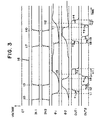
- the input signal IN1 shifts from the high level to the low level and the input signal IN2 shifts from the low level to the high level, at time t0.
- Those level shifts of the input signals IN1, IN2 are transferred through the D-FETs 14, 15 to the inputs of the latch circuit 13. Since the D-FETs 14, 15 are in the high impedance state according to the level of the control signal CT, the input signals IN1, IN2 slowly pass through the D-FETs 14, 15.
- the D-FET 16 is also in the high impedance state, so that the latch circuit 13 keeps the level difference between the two inputs thereof.
- the inverters 17, 18 While the level changes given to the latch circuit 13 are still small, the inverters 17, 18 are reluctant to flip their levels. However, once the input level surpasses the threshold level of the inverters 17, 18, the inverters 17, 18 vigorously change their output levels. Though the inverters 17, 18 are made in the same size, the inverter 18 begins to pull down the output ⁇ 1 thereof at time tl before the inverter 17 begins to pull up the output ⁇ 2 thereof at time t2, because those inverters 17, 18 are more sensitive to increasing of input levels than to decreasing of input levels.
- the output of the inverter 11 shifts from the low level to the high level at the end of period of time ⁇ 1 after time tl. Subsequently, the output of the inverter 12 shifts from the high level to the low level at the end of period of time ⁇ 2 after time t2. Even if the input signals IN1, IN2 are changed at the same time, the output signals OUT1, OUT2 are not changed at the same time, and time difference remains.
- the output ⁇ 1 is a little pulled down by the inverter 17 through the conducting D-FET 16
- the output ⁇ 2 is a little pulled up by the inverter 18 through the conducting D-FET 16.
- the levels of the outputs ⁇ 1, ⁇ 2 are determined in the proportion of impedance of the D-FET against impedance of the inverters 18, 17. Then, when the input signals IN1, IN2 shift at time t7 to the low level and to the high level, respectively, the inverters 17, 18 are activated to render the outputs ⁇ 1, ⁇ 2 low and high, respectively.
- the inverter 18 first becomes active, and subsequently, the inverter 17 becomes so, those inverters 17, 18 quickly responds to the level shifts of the inputs of the latch circuit 13, because the level difference between the inputs of the latch circuit 13 is already reduced by the conducting D-FET 16 that has been made low impedance by the control signal CT.
- the output of the inverter 11 shifts from the low level to the high level at the end of period of time ⁇ 3 after time t8.
- the output of the inverter 12 shifts from the high level to the low level at the end of period of time ⁇ 4 after time t9.
- the latch circuit 13 holds the signals in substantially same manner described above.
- the inverter 17 first begins to pull down the level of the output ⁇ 2, and then, the inverter 18 begins to pull up the level of the output ⁇ 2. Since the D-FET 16 is conducting with low impedance, the level difference between inputs of the latch circuit 13 is reduced, so that each of the inverters 17, 18 can quickly drive the output level.
- the output of the inverter 12 shifts from the low level to the high level at the end of period of time ⁇ 3 after time t11.
- the time difference ⁇ 2 between the changes of output signals OUT1, OUT2 where the control signal CT is at the high level becomes smaller than the time difference ⁇ 1 where the control signal CT is at the low level.
- the time difference ⁇ 2 can be much smaller when the D-FET 16 has significantly low impedance in comparison with impedance of the impedance of inverters 17, 18 and the D-FETs 14, 15.
- the D-FET 16 allows the level at the latch circuit 13 to shift quickly, the latch circuit 13 can easily change its state to the opposite state with small necessary energy.
- the variable delay circuit 10 can set the minimum delay time smaller than that of the conventional circuit, so that the variable delay circuit 10 can make the signal delay amount in a wide range.
- the energy required for changing the state of the latch circuit is energy for charging capacity of the gates and interconnections of the FETs in the latch circuit 13.
- the impedance of the D-FET 16 can be controlled so as to reduce or minimize the time difference between the two outputs OUT1, OUT2 of the variable delay circuit 10.
- the transfer gates of the variable delay circuit use only one transistor for each gate, so that the total number of the elements can be reduced to such as 11 elements and so that the variable delay circuit can be favorable to highly integrated circuit.
- variable delay circuit 10a is shown. Portions of the variable delay circuit 10a common to the portions of the variable delay circuit 10 are given the same reference numbers, and their detailed descriptions are omitted for the sake of simplicity.
- Inverters 21, 22 are two-input type instead of the single end type in the first embodiment.
- One input of the inverter 21 is coupled to the other of the source and drain of the D-FET 14 and to the output of the inverter 18; the other input of the inverter 21 is coupled to the output of the inverter 17.
- One input of the inverter 22 is coupled to the other of the source and drain of the D-FET 15 and to the output of the inverter 17; the other input of the inverter 21 is coupled to the output of the inverter 18.
- Fig. 5 shows circuitry of the inverter 21 in Fig. 4.
- a D-FET 54 and an E-FET 52 are connected in series between the power supply VDD and the ground GND.
- the gate 51 of the E-FET 52 is coupled to the output of the inverter 18.
- the gate 53 of the D-FET 54 is coupled to the output of the inverter 17.
- the source of the D-FET 54 and the drain of the E-FET are commonly connected to an output terminal 55 which constitutes the output terminal 34 for feeding the signal OUT1.
- the inverter 22 has the same constitution except that the gate 53 is coupled to the output of the inverter 18 and that the gate 51 is coupled to the output of the inverter 17.
- This variable delay circuit according to the second embodiment can precisely and coincidentally produce output signals whose state constitutes a logical complement of one another, though in the first embodiment as described above the time difference between the outputs may remain even if the input signals IN1, IN2 shift at the same time where the latch circuit 13 has different sensitivity between a transition from the high level to the low level and a transition from the low level to the high level.
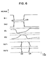
- the input signal IN1 shifts at time t21 from the high level to the low level, and at the same time, time t21, the input signal IN2 shifts from the low level to the high level.
- the inverter 18 first pulls down the output level ⁇ 1, and subsequently, the inverter 17 pulls up the output level ⁇ 2. After the inverter 18 pulls down the output level ⁇ 1 and before the inverter 17 pulls up the output level ⁇ 2, the E-FET 52 in the inverter 21 is turned off but the D-FET 54 in the inverter 21 is still in the high impedance state, so that the output signal OUT1 is reluctantly shifted to the high level.
- the D-FET 54 After the inverter 17 pulls up the output level ⁇ 2, the D-FET 54 now becomes the low impedance state, and therefore the D-FET 54 allow the current to flow into the output terminal 34 to make the output signal OUT1 at the high level.
- the E-FET 52 in the inverter 22 is also turned on to shift the output signal OUT2 to the low level. That is, unless both the output levels ⁇ 1, ⁇ 2 are adequately shifted, the level shifts of the output signals OUT1, OUT2 do not come out of the inverters 21, 22.
- variable delay circuit 10a uses two-input type inverters 21, 22 which allow the output signals change only after both outputs of the latch circuit 23 are established, so that the variable delay circuit 10a can nullify the time difference between the output signals OUT1, OUT2.
- the D-FET coupled between the inputs of the latch circuit allows the level at the latch circuit to quickly shift, so that the control signal is able to control the minimum delay time smaller than that of the conventional, and so that the variable range of delay time becomes wider.
- the delay circuit uses two-input inverters that become active only after two complementary outputs of the latch circuit are established, so that time difference between the outputs of the delay circuit is nullified or reduced.
- variable delay circuit solely formed is described in the embodiments above, a plurality of the variable delay circuits can be connected in series to produce a larger amount of delay time.
- the variable delay circuit can be used as a ring oscillator with variable oscillation frequency by connecting the noninverted input with the inverted output of one or more of the variable delay circuits.
- the D-FETs 14, 15 and 16 can be made of E-FETs, where the control signal CT controls the impedance of the E-FET.
- the delay circuit can reduce deviations of delay amounts due to fluctuations of the power supply VDD because the high level of the output signal of the inverters 21, 22 is fixed to a constant voltage thereby rendering the logical swings constant.
Landscapes
- Physics & Mathematics (AREA)
- Nonlinear Science (AREA)
- Engineering & Computer Science (AREA)
- Computer Hardware Design (AREA)
- Computing Systems (AREA)
- General Engineering & Computer Science (AREA)
- Mathematical Physics (AREA)
- Pulse Circuits (AREA)
- Manipulation Of Pulses (AREA)
Applications Claiming Priority (3)
| Application Number | Priority Date | Filing Date | Title |
|---|---|---|---|
| JP25818594 | 1994-10-24 | ||
| JP258185/94 | 1994-10-24 | ||
| JP6258185A JP3043241B2 (ja) | 1994-10-24 | 1994-10-24 | 可変遅延回路 |
Publications (3)
| Publication Number | Publication Date |
|---|---|
| EP0709960A2 true EP0709960A2 (de) | 1996-05-01 |
| EP0709960A3 EP0709960A3 (de) | 1997-03-19 |
| EP0709960B1 EP0709960B1 (de) | 2002-09-04 |
Family
ID=17316700
Family Applications (1)
| Application Number | Title | Priority Date | Filing Date |
|---|---|---|---|
| EP95307414A Expired - Lifetime EP0709960B1 (de) | 1994-10-24 | 1995-10-18 | Schaltung mit veränderlicher Verzögerung |
Country Status (4)
| Country | Link |
|---|---|
| US (1) | US5686851A (de) |
| EP (1) | EP0709960B1 (de) |
| JP (1) | JP3043241B2 (de) |
| KR (1) | KR100305230B1 (de) |
Cited By (1)
| Publication number | Priority date | Publication date | Assignee | Title |
|---|---|---|---|---|
| EP1326341A1 (de) * | 2001-12-20 | 2003-07-09 | Texas Instruments Limited | Ausgangstreiber mit gesteuerter Anstiegszeit |
Families Citing this family (2)
| Publication number | Priority date | Publication date | Assignee | Title |
|---|---|---|---|---|
| DE69700292T2 (de) * | 1997-11-18 | 1999-10-14 | Hewlett-Packard Co. | Veränderbare digitale Verzögerungszelle |
| US6182230B1 (en) * | 1998-10-02 | 2001-01-30 | International Business Machines Corporation | Active accelerated discharge of a capacitive system |
Family Cites Families (13)
| Publication number | Priority date | Publication date | Assignee | Title |
|---|---|---|---|---|
| US3821719A (en) * | 1970-06-12 | 1974-06-28 | Hitachi Ltd | Semiconductor memory |
| FR2262884B1 (de) * | 1974-03-01 | 1978-01-06 | Commissariat Energie Atomique | |
| US4593214A (en) * | 1984-01-05 | 1986-06-03 | Thomson Components - Mostek Corporation | Circuit for discharging bootstrapped nodes in integrated circuits with the use of transistors designed to withstand only the normal voltage |
| US4837465A (en) * | 1985-01-16 | 1989-06-06 | Digital Equipment Corp | Single rail CMOS register array and sense amplifier circuit therefor |
| US4864544A (en) * | 1986-03-12 | 1989-09-05 | Advanced Micro Devices, Inc. | A Ram cell having means for controlling a bidirectional shift |
| JPH077901B2 (ja) * | 1988-02-29 | 1995-01-30 | 沖電気工業株式会社 | フリップフロップ回路 |
| JP2540934B2 (ja) * | 1989-03-09 | 1996-10-09 | 三菱電機株式会社 | 論理回路装置 |
| JP2570471B2 (ja) * | 1990-06-25 | 1997-01-08 | 日本電気株式会社 | クロックドライバー回路 |
| JPH0478215A (ja) * | 1990-07-18 | 1992-03-12 | Sony Corp | マスタースレーブ型フリップフロップ回路 |
| US5281865A (en) * | 1990-11-28 | 1994-01-25 | Hitachi, Ltd. | Flip-flop circuit |
| JP2871087B2 (ja) * | 1990-11-30 | 1999-03-17 | 日本電気株式会社 | フリップフロップ回路 |
| JP3085803B2 (ja) * | 1992-11-26 | 2000-09-11 | 株式会社東芝 | 差動電流源回路 |
| US5495195A (en) * | 1994-11-17 | 1996-02-27 | Advanced Micro Devices, Inc. | Output buffer for a high density programmable logic device |
-
1994
- 1994-10-24 JP JP6258185A patent/JP3043241B2/ja not_active Expired - Fee Related
-
1995
- 1995-08-10 KR KR1019950024689A patent/KR100305230B1/ko not_active Expired - Fee Related
- 1995-10-05 US US08/539,685 patent/US5686851A/en not_active Expired - Lifetime
- 1995-10-18 EP EP95307414A patent/EP0709960B1/de not_active Expired - Lifetime
Cited By (1)
| Publication number | Priority date | Publication date | Assignee | Title |
|---|---|---|---|---|
| EP1326341A1 (de) * | 2001-12-20 | 2003-07-09 | Texas Instruments Limited | Ausgangstreiber mit gesteuerter Anstiegszeit |
Also Published As
| Publication number | Publication date |
|---|---|
| JP3043241B2 (ja) | 2000-05-22 |
| JPH08125507A (ja) | 1996-05-17 |
| KR960016142A (ko) | 1996-05-22 |
| KR100305230B1 (ko) | 2001-11-22 |
| EP0709960A3 (de) | 1997-03-19 |
| EP0709960B1 (de) | 2002-09-04 |
| US5686851A (en) | 1997-11-11 |
Similar Documents
| Publication | Publication Date | Title |
|---|---|---|
| EP0493873B1 (de) | CMOS-Ausgangspufferschaltung mit reduzierten Prellen auf den Masseleitungen | |
| EP0322447B1 (de) | Cmos-eingangspufferempfängerkreis | |
| KR100224138B1 (ko) | 출력 버퍼 회로 | |
| US4710650A (en) | Dual domino CMOS logic circuit, including complementary vectorization and integration | |
| US4554467A (en) | CMOS Flip-flop | |
| EP0405833A2 (de) | Eingangspuffer mit programmierbarem Eingangsschaltpegel | |
| US6927606B2 (en) | Low voltage differential to single-ended converter | |
| US5278467A (en) | Self-biasing input stage for high-speed low-voltage communication | |
| US5410189A (en) | Input buffer having an accelerated signal transition | |
| US20090091358A1 (en) | Compensated output buffer for improving slew control rate | |
| JP2004328443A (ja) | 半導体装置 | |
| US6236237B1 (en) | Output buffer predriver with edge compensation | |
| US6617881B2 (en) | Semiconductor integrated circuit | |
| US6958626B2 (en) | Off chip driver | |
| US5739701A (en) | Input/output buffer circuit having reduced power consumption | |
| US6323756B1 (en) | Data transmitter | |
| EP0488826A2 (de) | Flipflop-Schaltung mit einem CMOS-Hysterese-Inverter | |
| US4897567A (en) | Fast level translator circuit | |
| EP0709960B1 (de) | Schaltung mit veränderlicher Verzögerung | |
| US11271549B2 (en) | Semiconductor device for controlling voltage at an input node of a circuit during a low power mode | |
| US7030673B2 (en) | Phase splitter circuit | |
| US5767696A (en) | Tri-state devices having exclusive gate output control | |
| CN118151706A (zh) | 电路和操作电路的方法 | |
| US5495182A (en) | Fast-fully restoring polarity control circuit | |
| US6459307B2 (en) | Input buffer having dual paths |
Legal Events
| Date | Code | Title | Description |
|---|---|---|---|
| PUAI | Public reference made under article 153(3) epc to a published international application that has entered the european phase |
Free format text: ORIGINAL CODE: 0009012 |
|
| AK | Designated contracting states |
Kind code of ref document: A2 Designated state(s): FR GB SE |
|
| PUAL | Search report despatched |
Free format text: ORIGINAL CODE: 0009013 |
|
| AK | Designated contracting states |
Kind code of ref document: A3 Designated state(s): FR GB SE |
|
| 17P | Request for examination filed |
Effective date: 19970905 |
|
| GRAG | Despatch of communication of intention to grant |
Free format text: ORIGINAL CODE: EPIDOS AGRA |
|
| GRAG | Despatch of communication of intention to grant |
Free format text: ORIGINAL CODE: EPIDOS AGRA |
|
| GRAH | Despatch of communication of intention to grant a patent |
Free format text: ORIGINAL CODE: EPIDOS IGRA |
|
| 17Q | First examination report despatched |
Effective date: 20020125 |
|
| GRAH | Despatch of communication of intention to grant a patent |
Free format text: ORIGINAL CODE: EPIDOS IGRA |
|
| GRAA | (expected) grant |
Free format text: ORIGINAL CODE: 0009210 |
|
| AK | Designated contracting states |
Kind code of ref document: B1 Designated state(s): FR GB SE |
|
| REG | Reference to a national code |
Ref country code: GB Ref legal event code: FG4D |
|
| ET | Fr: translation filed | ||
| PLBE | No opposition filed within time limit |
Free format text: ORIGINAL CODE: 0009261 |
|
| STAA | Information on the status of an ep patent application or granted ep patent |
Free format text: STATUS: NO OPPOSITION FILED WITHIN TIME LIMIT |
|
| 26N | No opposition filed |
Effective date: 20030605 |
|
| PGFP | Annual fee paid to national office [announced via postgrant information from national office to epo] |
Ref country code: FR Payment date: 20031003 Year of fee payment: 9 |
|
| PGFP | Annual fee paid to national office [announced via postgrant information from national office to epo] |
Ref country code: SE Payment date: 20031007 Year of fee payment: 9 |
|
| PGFP | Annual fee paid to national office [announced via postgrant information from national office to epo] |
Ref country code: GB Payment date: 20031016 Year of fee payment: 9 |
|
| PG25 | Lapsed in a contracting state [announced via postgrant information from national office to epo] |
Ref country code: GB Free format text: LAPSE BECAUSE OF NON-PAYMENT OF DUE FEES Effective date: 20041018 |
|
| PG25 | Lapsed in a contracting state [announced via postgrant information from national office to epo] |
Ref country code: SE Free format text: LAPSE BECAUSE OF NON-PAYMENT OF DUE FEES Effective date: 20041019 |
|
| EUG | Se: european patent has lapsed | ||
| GBPC | Gb: european patent ceased through non-payment of renewal fee |
Effective date: 20041018 |
|
| PG25 | Lapsed in a contracting state [announced via postgrant information from national office to epo] |
Ref country code: FR Free format text: LAPSE BECAUSE OF NON-PAYMENT OF DUE FEES Effective date: 20050630 |
|
| REG | Reference to a national code |
Ref country code: FR Ref legal event code: ST |