EP0709971A2 - Convertisseur analogique-numérique sigma delta à trois points et méthode associée - Google Patents
Convertisseur analogique-numérique sigma delta à trois points et méthode associée Download PDFInfo
- Publication number
- EP0709971A2 EP0709971A2 EP95307582A EP95307582A EP0709971A2 EP 0709971 A2 EP0709971 A2 EP 0709971A2 EP 95307582 A EP95307582 A EP 95307582A EP 95307582 A EP95307582 A EP 95307582A EP 0709971 A2 EP0709971 A2 EP 0709971A2
- Authority
- EP
- European Patent Office
- Prior art keywords
- signal
- full scale
- offset
- positive
- negative
- Prior art date
- Legal status (The legal status is an assumption and is not a legal conclusion. Google has not performed a legal analysis and makes no representation as to the accuracy of the status listed.)
- Withdrawn
Links
Images


Classifications
-
- H—ELECTRICITY
- H03—ELECTRONIC CIRCUITRY
- H03M—CODING; DECODING; CODE CONVERSION IN GENERAL
- H03M3/00—Conversion of analogue values to or from differential modulation
- H03M3/30—Delta-sigma modulation
- H03M3/38—Calibration
-
- H—ELECTRICITY
- H03—ELECTRONIC CIRCUITRY
- H03M—CODING; DECODING; CODE CONVERSION IN GENERAL
- H03M1/00—Analogue/digital conversion; Digital/analogue conversion
- H03M1/06—Continuously compensating for, or preventing, undesired influence of physical parameters
- H03M1/0602—Continuously compensating for, or preventing, undesired influence of physical parameters of deviations from the desired transfer characteristic
- H03M1/0604—Continuously compensating for, or preventing, undesired influence of physical parameters of deviations from the desired transfer characteristic at one point, i.e. by adjusting a single reference value, e.g. bias or gain error
- H03M1/0607—Offset or drift compensation
-
- H—ELECTRICITY
- H03—ELECTRONIC CIRCUITRY
- H03M—CODING; DECODING; CODE CONVERSION IN GENERAL
- H03M3/00—Conversion of analogue values to or from differential modulation
- H03M3/30—Delta-sigma modulation
- H03M3/458—Analogue/digital converters using delta-sigma modulation as an intermediate step
Definitions
- This invention relates to Sigma Delta analog to digital converters (ADC), and, in particular, to an apparatus and a method relating to the integral non-linearity of Sigma-Delta ADCs through three point digital calibration.
- ADC Sigma Delta analog to digital converters
- Some ADCs make provision for correcting inherent errors. Such correction is commonly known as calibration which corrects for offset and gain errors. Offset is demonstrated by the ADC having a non-zero output when its input signal is zero or ground. In prior art devices the zero input is converted into a digital value, stored and is subtracted from all other digital values converted thereafter. Gain error is demonstrated by the ADC having a non-ideal output, i.e., different from all Is, when the full scale input signal is applied and offset error has been removed. In a similar manner prior art devices convert a positive reference voltage into a digital value that is offset corrected, and used to generate a gain correction factor. This gain correction factor is multiplied by all other offset corrected digital values converted thereafter.
- the ideal output for an ADC is all 1s when the input is at its full scale value. However, the actual noncalibrated full scale output of the ADC may be more or less, so its uncalibrated output is different from all is. In other words, instead of a slope of m, the slope is .5m or 1 .3m or some other value different from the ideal.
- the offset calibrated output of the ADC by a gain correction factor that is the quotient of a division where the numerator represents the total resolution of the converter and the denominator is the offset corrected digital code determined from a full scale input to the ADC.
- the result will be the maximum output, i.e. all 1s.
- the desired full scale output would be 111.
- the three bit ADC is designed to convert a full scale input of 2 volts to a digital signal. A full scale input of 2 volts should yield a digital output of 111.
- the Sigma Delta modulator is the critical component in determining accuracy and linearity.
- the principal sources of non-linearity have been identified as the voltage coefficient of the capacitors (1 st and 2nd order, primarily) as well as integrator leakage. Integrator leakage is due to finite integrator DC gain. This can be overcome by designing an integrator with sufficient gain for a particular application.
- Nonlinearity due to capacitor voltage coefficient can be addressed, to a certain extent, with a fully differential modulator structure.
- the hilly differential signal paths allow the cancellation of first order nonlinearity due to the first order capacitor coefficient.
- the second order voltage coefficient will generate nonlinearities since they are not cancelled by these signal paths.
- the invention provides an ADC with a Sigma Delta modulator, with n bit resolutionand with three point calibration of a digitally filtered output of a bipolar analog signal.
- the three points of calibration include offset at the bipolar midscale point, positive full scale and negative full scale.
- the analog modulator has its output applied to a digital filter.
- the output of the digital filter is calibrated to correct for offset and for bipolar gain variations.
- the analog modulator has input reference signals corresponding to ground or zero. a positive reference signal and a negative reference signal.
- the ground reference signal is coupled to the input of the analog modulator to generate a digital offset correction signal.
- the digital offset correction signal is stored in an offset correction register.
- the value of the offset correction may be positive or negative.
- the value of the offset correction register is subtracted from the digital filter output for each conversion.
- the ADC has separate gain correction factors for positive and negative inputs.
- the positive reference signal is coupled to the input of the analog modulator to generate an uncalibrated positive full scale digital output signal.
- the offset correction is applied to the uncalibrated output signal to provide a positive full scale digital output signal.
- the positive full scale digital output signal is stored in a positive full scale register.
- the positive gain correction factor is provided by dividing half of the resolution of the desired full scale output of the ADC by the contents stored in the positive full scale register. Since there are separate corrections for positive and negative signals, half the resolution is used to correct for signals of one polarity and the other half of the resolution is used to correct for signals of the opposite polarity.
- the positive gain correction factor is stored in its own register while needed.
- the negative input correction factor is formed in a similar manner.
- the negative reference signal is coupled to the input of the analog modulator to generate an uncalibrated negative full scale digital output signal.
- the offset correction is applied to the uncalibrated negative full scale digital output signal to provide a negative full scale digital output signal.
- the negative full scale digital output signal is stored in a negative full scale register.
- the negative gain correction factor is provided by dividing half of the resolution of the desired full scale register by the contents stored in the negative full scale register. The negative gain correction factor is stored only while it is needed.
- an input analog signal is applied to the analog modulator.
- the output of the modulator is coupled to the digital filter and the digital filter provides an uncorrected digital signal to a summing node.
- the digital filter output is a digital signal representative of the applied analog voltage.
- a summing node applies the offset correction signal stored in the offset correction register to the uncorrected digital signal.
- the offset corrected digital signal is multiplied by the positive or negative gain correction factor to yield a calibrated, corrected digital output signal. It is also possible to perform the gain correction directly on the offset corrected signal.
- the offset corrected signal may be multiplied by half the full scale resolution of the ADC and divided by the signal in the positive or negative full scale register.
- the invention also relies upon a 2's compliment coding so the most significant bit indicates the polarity of the offset corrected digital signal.
- the analog modulator has a differential input with positive and negative terminals.
- the invention couples a positive reference voltage to the negative differential input and couples a zero or ground voltage to the positive differential input to emulate a negative reference signal. So, the invention eliminates the need for separate reference signals by allowing both positive and negative gain correction factors to be generated from the positive reference signal.
- the present invention includes a Sigma Delta ADC with n bit resolution and three point calibration comprising:
- the invention also includes a method for three point calibration of an analog to digital converter with a Sigma Delta modulator with n bit resolution comprising the steps' of:
- FIG. 1 shows an ADC 10 with a switched capacitor analog is modulator 12.
- the analog modulator inputs are fully differential.
- the input voltage VIN is coupled to differential input terminals 5, 6.
- three additional voltage signals are shown as inputs to the analog modulator 12. These inputs, V H(+)5 , V L(-)5 , and V GND are shown for clarity of discussion only and are not actual inputs to the modulator.
- the signal V H(+) is a positive full scale reference voltage signal that in actual design practice can be generated by placing the most positive voltage the ADC can convert on terminal 5 (VIN+) and grounding terminal 6 (V IN ).
- the signal V L(-) is a negative full scale reference voltage signal that in actual design practice can be generated by placing the most negative voltage the ADC can convert on terminal 6 (V IN ) and grounding terminal 5 (V IN + ).
- the signal V GND is a zero scale reference voltage signal that in actual design practice can be generated by shorting terminal 5 (V IN + ) to terminal 6 (V IN .).
- Suitable circuitry could supply a negative full scale reference voltage by placing a positive reference voltage on the input terminal 6 (V IN- ) and grounding the other input terminal 5 (V IN+ ).
- the output of the analog modulator 12 is a converted digital signal that is coupled' to a digital filter 14.
- the output of the digital filter 14 is coupled to a summing node 18.
- the output of the digital filter 14 is corrected for offset.
- the offset corrected digital signal is input to a multiplier 20. In the multiplier 20 the offset corrected digital signal is gained corrected to provide the digital output signal D OUT .
- Controller 16 controls the operation of the ADC 10 and, in particular, the switched capacitor analog modulator 12, digital filter 14, the summing node 18, multiplier 20, and divider 30.
- the controller 16 has control lines 31-46, 55-58 for carrying control signals to the components of the ADC 10. Accordingly, the controller 16 controls division operations and multiplication operations on digital signals to generate gain correction factors for positive and negative input signals when the ADC 10 operates in its bipolar mode and another gain correction factor for unipolar mode.
- Offset correction register (OCR) 22 stores a digital signal representative of the offset error of the ADC 10. OCR 22 receives the output of the filter 14 via data line 70 when V IN is set to V GND .
- Controller 16 is also coupled to a positive full scale correction register (PFSCR) 24 and a negative full scale correction register (NFSCR) 26, and to a desired full scale register 28.
- the desired full scale register (DFSR) 28 holds a digital value corresponding to half the resolution of the ADC 10.
- the DFSR 28 is a single bit register. Since the value of DFSR 28 always the maximum digital signal output code, the DFSR 28 can be one bit which is continuously set to a predetermined value for each adding and subtracting operation as will be further explained hereinafter.
- the DFRSR 28 contains a digital signal representing one half of the resolution of the converter 10 for bipolar operation and representing the full resolution of the converter 10 for unipolar operation.
- Data path line 59 carries the offset corrected full scale signal from the output of summing node 18 for storage in the appropriate register 24, 26.
- the positive full scale correction register 24 holds a digital signal corresponding to the voltage appearing at the output of the summing node 18 after the reference voltage V H(+) is applied to the analog modulator 12.
- the negative full scale register (NFSCR) 26 holds a digital signal corresponding to the output of summing node 18 when the negative reference voltage V L (-) 15 applied to the analog modulator 12 and converted to a digital signal.
- the controller 16 is coupled via control line 33 and line 37 to a selector 29.
- the selector 29 applies the value of the PFSCR 24 or the NFSCR 26 to the denominator of a divider 30.
- the numerator of the divider 30 receives the output the DFSR 28. As such, the value in the divider 30 corresponds to the correction value for the gain of the ADC 10. This correction value may be stored in a correction factor register 46.
- the correction factor register 46 is also controlled by controller 16 via control line 55.
- the analog modulator 12 is a typical Sigma Delta modulator well known to those skilled in the art. Analog modulator 12 performs a one bit A to D conversion. The analog modulator 12 uses a switch capacitor charge balancing circuit for performing sequential one bit conversions of the input signal V IN . In operation the input signal V IN is switched across an integrating amplifier. The integrating amplifier outputs a ramp type function since it sees a step type input. When the ramp function output of the integrator reaches a predetermined value of one bit, the digital value is applied to a summing node that subtracts the equivalent voltage corresponding to one bit from the input signal V IN . As such, the analog modulator 12 provides a series of digital output values (I or 0) that are input to a digital low pass filter 14.
- I or 0 digital output values
- the filter 14 is coupled to a timer (not shown) that is run by a clock (not shown) provided by the controller 16.
- the combination of the timer and the low pass filter 14 are used to provide an output representative of the average number of ones in the input signal V IN .
- the digital filter 14 removes out-of-band quantization noise, sample rate reduction and interference from 50/60 Hz noise.
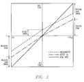
- Figure 2 shows a first curve A.
- Curve A is the uncalibrated digital representation of the applied input voltage, VIN.
- Curve B is the offset corrected digital representation of the applied input voltage, VIN.
- Curve B has one slope for positive voltages and a different slope for negative voltages.
- Curve C represents the ideal transfer function of the ADC. The difference between curve 3 and curve C is due to gain nonidealities in the analog modulator and digital filter. As seen, there is a positive offset when the input voltage, V IN , is zero and the slope of the uncalibrated data is different for negative versus positive voltages. In an offset calibration operation, the zero or ground reference signal is coupled to the input of the analog modulator 12.
- the uncalibrated digital output of filter 14 is stored in the OCR 22 and is subtracted from the uncalibrated digital representation of all conversions' thereafter. This is represented by curve B of Figure 2.
- Gain correction requires the offset corrected digital representation be multiplied by a 10 gain slope factor. Two gain slope factors are generated, one for positive voltages (after offset correction), the other for negative voltages (after offset correction).
- the positive reference signal Y L(-) is coupled to the input of the analog modulator to generate an uncalibrated positive full scale digital output signal.
- the offset correction in OCR 22 is applied to the uncalibrated positive full scale digital output signal to provide a positive full scale digital output signal.
- the positive full scale digital output signal is stored in PFSCR 24.
- the negative reference signal VL(.) is coupled to 20 the input of the analog modulator 12 to generate an uncalibrated negative full scale digital output signal.
- the offset correction in OCR 22 is applied to the uncalibrated negative full scale digital output signal to provide a negative full scale digital output signal.
- the negative full scale digital output signal is stored in a NFSCR 26.
- the offset calibrated digital signal is inspected for polarity and multiplied by the proper gain slope factor. If the polarity of the offset corrected data indicates a positive voltage is being converted, the positive gain slope factor is generated by dividing the contents of the DFSR 28 value by the PFSCR 24 value and multiplying that quotient by the offset corrected digital signal. If the polarity indicates a negative voltage is being converted, the negative gain slope factor is generated by dividing the contents of the DFSR 28 value by the NFSCR 26 value and multiplying that quotient by the offset corrected digital signal.
- the ADC 10 records the filter 14 output under three different input conditions.
- a zero scale input, VoND is used to eliminate offset error
- a positive full scale input V H(+) is used to eliminate gain error for positive input voltages
- a negative full scale input V L(+) is used to eliminate gain error for negative input voltages.
- the ADC 10 automatically selects the proper gain slope factor depending on the offset corrected data. If the offset corrected data is positive, representing a positive voltage, the positive gain slope factor is used. If the offset corrected data is negative, representing a negative voltage, the negative gain slope factor is used.
- step 60 the steps required for calibrating the output of the digital filter begin with a start calibration step 60.
- step 61 removes offset error.
- step 62 determines in step 62 whether the ADC 10 is set up for bipolar or unipolar operation. If bipolar operation is active, then in step 63, the polarity of the offset corrected digital signal is determined.
- step 63 if the polarity of the offset corrected data indicates a positive voltage is being converted, the positive gain slope factor is generated by dividing the contents of the desired full scale register value by the positive full scale register value.
- step 63 If the polarity indicates a negative voltage is being converted, the negative gain slope factor is generated by dividing the contents of the desired full scale register value by the negative full scale register value.
- step 65 the gain slope factor generated in step 63 is multiplied by the offset corrected digital signal, completing calibration.
- the unipolar mode branch comprises steps 64 and 68 that are similar to steps 63, 65 except, by definition, only the positive gain slope factor will be generated.
- Equation 1 mathematically describes the bipolar three point calibration operation.
- D OUT slope (V iN - Offset), where Offset is contents of the OCR 22
- Slope varies with the mode of operation and the polarity of the input signal.
- first slope ⁇ i for positive input signals and S1
- second slope 22 for negative input signals is one half the resolution of the converter 10 divided by the NFSCR 28 value.
- second slope 22 for negative input signals is one half the resolution of the converter 10 divided by the NFSCR 28 value.
- third slope S3 that is the full resolution of the converter 10 divided by the value in the PFSCR 24.
- Offset calibration is identical for bipolar or unipolar modes.
- the gain calibration function comprises four functional blocks. They are the full scale 10 calibration registers (PFSCR 24, NFSCR 26), the multiply logic 20, and divide logic 30.
- PFSCR 24, NFSCR 26 the full scale 10 calibration registers
- the multiply logic 20 the divide logic 30.
- V H(+) the positive full scale reference voltage
- the PFSCR 24 is updated with offset corrected data for V (+) .
- the negative full scale reference voltage V L(-) is presented to the analog modulator.
- the NFSCR 26 is updated with offset corrected data for V L(-) .
- the values in registers 24, 20 are used to calculate the proper gain slope factor for each conversion result.
- the ADC 10 determines which gain slope factor to use for each valid conversion. If the offset corrected data output from the summing node 18 is negative, the NFSCR 26 value is used to determine the gain slope factor. If the offset corrected data is positive, the PFSCR 24 value is used to determine the gain slope factor.
- the proper gain slope factor is not permanently stored but is generated for each conversion. That is, after receiving offset calibrated data for non calibration conversion, the controller 16 selects the proper calibration register and completes the division routine that calculates the gain slope factor. After determining the gain slope factor, the multiplication of the offset corrected data by that gain slope factor occurs, completing calibration.
- Gain calibration requirements are different for bipolar versus unipolar mode.
- unipolar mode the calibration logic determines the slope factor by dividing the total resolution of the converter (2 N ), where n is the number of bits in the output of the signal D OUT by the span between the zero and positive full scale points.
- bipolar mode the gain factor is determined by dividing one half the total resolution (2 N-1 ) of the converter by the span between the zero and positive or negative full scale points. In either unipolar or bipolar mode this division result is multiplied by the offset corrected filter output to calculate the proper binary output for the ADC 10.
- Division logic is used to calculate the gain factor discussed above.
- the divider 30 is activated after each valid conversion has completed.
- a valid conversion is defined as having removed offset error from digital filter 14 output for any non-calibration conversion.
- the result of the division is stored in a bidirectional shift register 46 used during the multiplication sequence.
- the numerator N of divider 30 for all divides in bipolar mode is fixed and is 2 N - 1 .
- the denominator D is either the PFSCR 24 value or the two's complement of the NFSCR 26.
- the two's complement of the N FSCR 26 represents the absolute value of the N FSCR 26 and is required as the division algorithin requires unsigned numbers.
- a 24 bit ADC 10 operating in its bipolar mode.
- the quotient of divider 30 is stored in register 46 as a binary number with three bits left of the binary point and 25 bits to the right of the binary point.
- the latter selection of the binary point can be varied, and is given only as a representative example of one embodiment.
- the division control logic in controller 16 is altered to multiply the final division' result by two. This is required since 24 cannot be represented in 24 bits. Using 24-2 x 23, it is valid to multiply the division result (in unipolar mode) by two.
- the quotient is stored as a binary number with three bits left of the binary point and 25 bits to the right of the binary point, its just that the answer is two times what one would expect given the raw data.
- the division function described above assumes unsigned numbers and as implemented in divider 30 is a shift-subtract algorithm similar to shift-add multiplication.
- the division result is generated by comparing the divisor to the current remainder. If the divisor is less than or equal to the current remainder, the result is one and the divisor is subtracted from the current remainder. The new remainder is that substraction result shifted left and appended with the next numerator bit. If the divisor is greater than the remainder, the result is zero and zero is subtracted from the current remainder. The new remainder is that subtraction result shifted left and appended with the next numerator bit.
- the quotient is stored as a binary number with three bits left of the binary point and 25 bits to the right of the binary point in register 46.
- the quotient In unipolar mode, the quotient is 2x23/PFSCR.
- the quotient In bipolar mode, the quotient is 2exp23/FSCR, where FSCR can be either PFCSR or NFSCR.
- the offset corrected data from the filter 14 is multiplied by the slope factor to complete calibration of the output.
- the multiplier 20 of the ADC 10 performs a serial shift-add multiply.
- An analog to digital converter 10 has a switched capacitor analog modulator 12 with three point calibration. Offset calibration applies on offset correction value in OCR 22 to an uncalibrated digital output. Register 28 holds a desired full scale value, register 24 holds a positive full scale value, and register 26 holds a negative full scale value. Depending upon the polarity of the converted analog signal, the offset corrected digital signal is multiplied by a positive or a negative gain correction factor.
Landscapes
- Engineering & Computer Science (AREA)
- Theoretical Computer Science (AREA)
- Compression, Expansion, Code Conversion, And Decoders (AREA)
- Analogue/Digital Conversion (AREA)
Applications Claiming Priority (2)
| Application Number | Priority Date | Filing Date | Title |
|---|---|---|---|
| US331015 | 1994-10-28 | ||
| US08/331,015 US5598157A (en) | 1994-10-28 | 1994-10-28 | Sigma Delta analog to digital converter with three point calibration apparatus and method |
Publications (2)
| Publication Number | Publication Date |
|---|---|
| EP0709971A2 true EP0709971A2 (fr) | 1996-05-01 |
| EP0709971A3 EP0709971A3 (fr) | 1998-05-06 |
Family
ID=23292271
Family Applications (1)
| Application Number | Title | Priority Date | Filing Date |
|---|---|---|---|
| EP95307582A Withdrawn EP0709971A3 (fr) | 1994-10-28 | 1995-10-25 | Convertisseur analogique-numérique sigma delta à trois points et méthode associée |
Country Status (5)
| Country | Link |
|---|---|
| US (1) | US5598157A (fr) |
| EP (1) | EP0709971A3 (fr) |
| KR (1) | KR960016157A (fr) |
| IL (1) | IL115631A (fr) |
| TW (1) | TW290763B (fr) |
Families Citing this family (37)
| Publication number | Priority date | Publication date | Assignee | Title |
|---|---|---|---|---|
| US5838598A (en) * | 1995-12-12 | 1998-11-17 | Analog Devices, Inc. | Method and apparatus for gain correction of a sigma-delta converter |
| FR2755324B1 (fr) * | 1996-10-25 | 1999-01-08 | Thomson Multimedia Sa | Conversion d'un signal analogique en signal numerique en particulier un signal video de tv |
| US6307891B1 (en) | 1997-04-22 | 2001-10-23 | Silicon Laboratories, Inc. | Method and apparatus for freezing a communication link during a disruptive event |
| US6456712B1 (en) | 1997-04-22 | 2002-09-24 | Silicon Laboratories Inc. | Separation of ring detection functions across isolation barrier for minimum power |
| US6359983B1 (en) | 1997-04-22 | 2002-03-19 | Silicon Laboratories, Inc. | Digital isolation system with data scrambling |
| US6385235B1 (en) | 1997-04-22 | 2002-05-07 | Silicon Laboratories, Inc. | Direct digital access arrangement circuitry and method for connecting to phone lines |
| US6480602B1 (en) | 1997-04-22 | 2002-11-12 | Silicon Laboratories, Inc. | Ring-detect interface circuitry and method for a communication system |
| US6442271B1 (en) | 1997-04-22 | 2002-08-27 | Silicon Laboratories, Inc. | Digital isolation system with low power mode |
| US6339048B1 (en) * | 1999-12-23 | 2002-01-15 | Elementis Specialties, Inc. | Oil and oil invert emulsion drilling fluids with improved anti-settling properties |
| US6389134B1 (en) | 1997-04-22 | 2002-05-14 | Silicon Laboratories, Inc. | Call progress monitor circuitry and method for a communication system |
| US6137827A (en) * | 1997-04-22 | 2000-10-24 | Silicon Laboratories, Inc. | Isolation system with digital communication across a capacitive barrier |
| US6298133B1 (en) | 1997-04-22 | 2001-10-02 | Silicon Laboratories, Inc. | Telephone line interface architecture using ringer inputs for caller ID data |
| US5870046A (en) | 1997-04-22 | 1999-02-09 | Silicon Laboratories Inc. | Analog isolation system with digital communication across a capacitive barrier |
| US6498825B1 (en) | 1997-04-22 | 2002-12-24 | Silicon Laboratories Inc. | Digital access arrangement circuitry and method for connecting to phone lines having a DC holding circuit with programmable current limiting |
| US6289070B1 (en) | 1997-04-22 | 2001-09-11 | Silicon Laboratories, Inc. | Digital isolation system with ADC offset calibration including coarse offset |
| US6167134A (en) | 1997-04-22 | 2000-12-26 | Silicon Laboratories, Inc. | External resistor and method to minimize power dissipation in DC holding circuitry for a communication system |
| US6430229B1 (en) | 1997-04-22 | 2002-08-06 | Silicon Laboratories Inc. | Capacitive isolation system with digital communication and power transfer |
| US6587560B1 (en) | 1997-04-22 | 2003-07-01 | Silicon Laboratories Inc. | Low voltage circuits powered by the phone line |
| US6516024B1 (en) | 1997-04-22 | 2003-02-04 | Silicon Laboratories Inc. | Digital access arrangement circuitry and method for connecting to phone lines having a DC holding circuit with low distortion and current limiting |
| US6144326A (en) | 1997-04-22 | 2000-11-07 | Silicon Laboratories, Inc. | Digital isolation system with ADC offset calibration |
| US6408034B1 (en) | 1997-04-22 | 2002-06-18 | Silicon Laboratories, Inc. | Framed delta sigma data with unlikely delta sigma data patterns |
| US6504864B1 (en) | 1997-04-22 | 2003-01-07 | Silicon Laboratories Inc. | Digital access arrangement circuitry and method for connecting to phone lines having a second order DC holding circuit |
| US6442213B1 (en) * | 1997-04-22 | 2002-08-27 | Silicon Laboratories Inc. | Digital isolation system with hybrid circuit in ADC calibration loop |
| US6255970B1 (en) * | 1997-10-10 | 2001-07-03 | Photobit Corporation | Correction of missing codes nonlinearity in A to D converters |
| US6008685A (en) * | 1998-03-25 | 1999-12-28 | Mosaic Design Labs, Inc. | Solid state temperature measurement |
| US6351228B1 (en) * | 1999-02-03 | 2002-02-26 | Hitachi Electronics Engineering Co., Ltd. | Digital calibration method and apparatus for A/D or D/A converters |
| US6384755B1 (en) * | 1999-04-09 | 2002-05-07 | Hewlett-Packard Company | Method and apparatus for analog to digital conversion using an impedance device as an identifier |
| US6411232B1 (en) | 1999-09-30 | 2002-06-25 | Motorola, Inc. | Method and system for determining an element conversion characteristic contemporaneous with converting and input signal in a signal converter |
| US6608580B2 (en) | 2001-02-15 | 2003-08-19 | Sarnoff Corporation | Differential analog-to-digital converter |
| US6924755B1 (en) | 2002-12-02 | 2005-08-02 | Analog Devices, Inc. | Multi-channel analog to digital converter which facilitates calibration of the analog to digital converter and respective input channels to the analog to digital converter, and a method for calibrating the analog to digital converter |
| KR100688520B1 (ko) * | 2005-01-17 | 2007-03-02 | 삼성전자주식회사 | 아날로그 디지털 컨버터의 캘리브레이션 방법 |
| JP2012165169A (ja) * | 2011-02-07 | 2012-08-30 | Renesas Electronics Corp | A/d変換器及び半導体装置 |
| JP5870699B2 (ja) * | 2012-01-10 | 2016-03-01 | ミツミ電機株式会社 | センサ出力補正回路及びセンサ出力補正装置、並びにセンサ出力補正方法 |
| US8847804B2 (en) * | 2012-11-05 | 2014-09-30 | Freescale Semiconductor, Inc. | Delay compensated continuous time sigma delta analog-to-digital converter |
| US9438266B1 (en) | 2016-02-10 | 2016-09-06 | Texas Instruments Incorporated | Calibrated-output analog-to-digital converter apparatus and methods |
| US9843337B1 (en) * | 2017-03-16 | 2017-12-12 | Analog Devices Global | Background flash offset calibration in continuous-time delta-sigma ADCS |
| CN117728838B (zh) * | 2024-02-08 | 2024-05-28 | 深圳市山海半导体科技有限公司 | 用于adc失调误差的模数转换装置与校准方法 |
Citations (3)
| Publication number | Priority date | Publication date | Assignee | Title |
|---|---|---|---|---|
| US4918434A (en) | 1982-12-22 | 1990-04-17 | Nintendo Co., Ltd. | T.V. game system |
| US4943807A (en) | 1988-04-13 | 1990-07-24 | Crystal Semiconductor | Digitally calibrated delta-sigma analog-to-digital converter |
| US5303004A (en) | 1988-02-19 | 1994-04-12 | Canon Kabushiki Kaisha | Apparatus for driving image bearing member via torque limiter |
Family Cites Families (17)
| Publication number | Priority date | Publication date | Assignee | Title |
|---|---|---|---|---|
| NL7512886A (nl) * | 1975-11-04 | 1977-05-06 | Hollandse Signaalapparaten Bv | Analoog-digitaal omzetter. |
| US4280196A (en) * | 1979-11-14 | 1981-07-21 | Hewlett-Packard Company | Correction of zero drift, gain drift, and distortion errors in analog storage devices |
| US4799041A (en) * | 1986-10-06 | 1989-01-17 | Applied Automation, Inc. | Recirculating analog to digital converter with auto-calibrating feature |
| US4947168A (en) * | 1988-05-23 | 1990-08-07 | Hughes Aircraft Company | Subranging analog-to-digital converter with calibration |
| US4918454A (en) * | 1988-10-13 | 1990-04-17 | Crystal Semiconductor Corporation | Compensated capacitors for switched capacitor input of an analog-to-digital converter |
| US4894656A (en) * | 1988-11-25 | 1990-01-16 | General Electric Company | Self-calibrating pipelined subranging analog-to-digital converter |
| JPH03205921A (ja) * | 1990-01-08 | 1991-09-09 | Hitachi Denshi Ltd | デジタイザ回路 |
| US5087914A (en) * | 1990-08-22 | 1992-02-11 | Crystal Semiconductor Corp. | DC calibration system for a digital-to-analog converter |
| US5172115A (en) * | 1991-02-15 | 1992-12-15 | Crystal Semiconductor Corporation | Ratiometric A/D converter with non-rationometric error offset |
| US5248970A (en) * | 1991-11-08 | 1993-09-28 | Crystal Semiconductor Corp. | Offset calibration of a dac using a calibrated adc |
| US5266952A (en) * | 1992-03-30 | 1993-11-30 | Hughes Aircraft Company | Feed forward predictive analog-to-digital converter |
| US5257026A (en) * | 1992-04-17 | 1993-10-26 | Crystal Semiconductor, Inc. | Method and apparatus for calibrating a multi-bit delta-sigma modular |
| US5206602A (en) * | 1992-04-30 | 1993-04-27 | Hewlett-Packard Company | Biomedical amplifier circuit |
| US5337230A (en) * | 1992-04-30 | 1994-08-09 | Hewlett-Packard Company | Signal processing circuits with digital programmability |
| EP0571075B1 (fr) * | 1992-04-30 | 1999-07-21 | Hewlett-Packard Company | Convertisseur analogique-numérique à réglage automatique de gamme de décalage |
| US5305004A (en) * | 1992-09-29 | 1994-04-19 | Texas Instruments Incorporated | Digital to analog converter for sigma delta modulator |
| US5465092A (en) * | 1994-01-19 | 1995-11-07 | National Semiconductor Corporation | Pipelined analog-to-digital converter with curvefit digital correction |
-
1994
- 1994-10-28 US US08/331,015 patent/US5598157A/en not_active Expired - Lifetime
-
1995
- 1995-10-13 IL IL11563195A patent/IL115631A/xx not_active IP Right Cessation
- 1995-10-24 KR KR1019950036827A patent/KR960016157A/ko not_active Abandoned
- 1995-10-25 EP EP95307582A patent/EP0709971A3/fr not_active Withdrawn
- 1995-10-28 TW TW084111396A patent/TW290763B/zh active
Patent Citations (3)
| Publication number | Priority date | Publication date | Assignee | Title |
|---|---|---|---|---|
| US4918434A (en) | 1982-12-22 | 1990-04-17 | Nintendo Co., Ltd. | T.V. game system |
| US5303004A (en) | 1988-02-19 | 1994-04-12 | Canon Kabushiki Kaisha | Apparatus for driving image bearing member via torque limiter |
| US4943807A (en) | 1988-04-13 | 1990-07-24 | Crystal Semiconductor | Digitally calibrated delta-sigma analog-to-digital converter |
Also Published As
| Publication number | Publication date |
|---|---|
| EP0709971A3 (fr) | 1998-05-06 |
| US5598157A (en) | 1997-01-28 |
| IL115631A0 (en) | 1996-01-19 |
| TW290763B (fr) | 1996-11-11 |
| KR960016157A (ko) | 1996-05-22 |
| IL115631A (en) | 1999-03-12 |
Similar Documents
| Publication | Publication Date | Title |
|---|---|---|
| US5598157A (en) | Sigma Delta analog to digital converter with three point calibration apparatus and method | |
| US7825837B1 (en) | Background calibration method for analog-to-digital converters | |
| US7501965B2 (en) | Correcting for errors that cause generated digital codes to deviate from expected values in an ADC | |
| US9041569B2 (en) | Method and apparatus for calibration of successive approximation register analog-to-digital converters | |
| EP0730794B1 (fr) | Architecture efficace de correction des defauts de non-concordance des composants et des non-linearites des circuits d'un convertisseur a/d | |
| KR100928406B1 (ko) | 증분-델타 아날로그-대-디지털 변환 | |
| EP0698315B1 (fr) | Convertisseur a/n algorithmique a signal de sortie a etalonnage numerique | |
| CN1036751C (zh) | 经调制的颤抖信号 | |
| EP0740862B1 (fr) | Convertisseur analogique/numerique pipeline avec correction numerique a ajustement de courbe | |
| US6222471B1 (en) | Digital self-calibration scheme for a pipelined A/D converter | |
| GB2266205A (en) | Calibrating a multi-bit delta-sigma modulator | |
| US5103230A (en) | Precision digitized current integration and measurement circuit | |
| US20020014982A1 (en) | A/D converter calibration | |
| US8742961B2 (en) | Gain and dither capacitor calibration in pipeline analog-to-digital converter stages | |
| EP0488818B1 (fr) | Convertisseur analogique/numérique | |
| US20050137802A1 (en) | Continuous digital background calibration in pipelined ADC architecture | |
| EP0553090B1 (fr) | Convertisseur analogique/numerique ou numerique/analogique, systeme de conversion analogique/numerique et numerique/analogique, et procede d'etalonnage correspondant | |
| US5146223A (en) | Analog-to-digital converter circuit | |
| EP1510007B1 (fr) | Systeme de calibrage de decalage | |
| WO2016056889A1 (fr) | Convertisseur analogique-numérique à approximations successives et son procédé d'étalonnage | |
| EP2351225B1 (fr) | Calibration de convertisseurs A/N série-séquentiels | |
| US5838598A (en) | Method and apparatus for gain correction of a sigma-delta converter | |
| US6522276B2 (en) | System of DAC correction for a ΔΣ modulator | |
| RU2335844C2 (ru) | Аналого-цифровой преобразователь и способ его калибровки | |
| KR880003485A (ko) | 에러검출 및 교정시스템을 갖춘 주기형 d/a 변환기 |
Legal Events
| Date | Code | Title | Description |
|---|---|---|---|
| PUAI | Public reference made under article 153(3) epc to a published international application that has entered the european phase |
Free format text: ORIGINAL CODE: 0009012 |
|
| AK | Designated contracting states |
Kind code of ref document: A2 Designated state(s): DE FR GB IT SE |
|
| PUAL | Search report despatched |
Free format text: ORIGINAL CODE: 0009013 |
|
| AK | Designated contracting states |
Kind code of ref document: A3 Designated state(s): DE FR GB IT SE |
|
| 17P | Request for examination filed |
Effective date: 19981106 |
|
| 17Q | First examination report despatched |
Effective date: 20020124 |
|
| GRAH | Despatch of communication of intention to grant a patent |
Free format text: ORIGINAL CODE: EPIDOS IGRA |
|
| STAA | Information on the status of an ep patent application or granted ep patent |
Free format text: STATUS: THE APPLICATION HAS BEEN WITHDRAWN |
|
| 18W | Application withdrawn |
Effective date: 20030623 |