EP0709975B1 - Verfahren und Gerät zur Burst-Detektion - Google Patents
Verfahren und Gerät zur Burst-Detektion Download PDFInfo
- Publication number
- EP0709975B1 EP0709975B1 EP95116694A EP95116694A EP0709975B1 EP 0709975 B1 EP0709975 B1 EP 0709975B1 EP 95116694 A EP95116694 A EP 95116694A EP 95116694 A EP95116694 A EP 95116694A EP 0709975 B1 EP0709975 B1 EP 0709975B1
- Authority
- EP
- European Patent Office
- Prior art keywords
- burst
- signal
- average
- filter
- received signal
- Prior art date
- Legal status (The legal status is an assumption and is not a legal conclusion. Google has not performed a legal analysis and makes no representation as to the accuracy of the status listed.)
- Expired - Lifetime
Links
- 238000000034 method Methods 0.000 title claims description 6
- 238000001514 detection method Methods 0.000 claims abstract description 37
- 230000003111 delayed effect Effects 0.000 claims abstract description 18
- 238000001914 filtration Methods 0.000 claims description 4
- 238000013459 approach Methods 0.000 description 18
- 238000010586 diagram Methods 0.000 description 12
- 230000001934 delay Effects 0.000 description 9
- 238000004891 communication Methods 0.000 description 5
- 230000000875 corresponding effect Effects 0.000 description 3
- 238000001228 spectrum Methods 0.000 description 3
- 239000013078 crystal Substances 0.000 description 2
- 230000007423 decrease Effects 0.000 description 2
- 238000012545 processing Methods 0.000 description 2
- 230000005540 biological transmission Effects 0.000 description 1
- 230000015556 catabolic process Effects 0.000 description 1
- 230000001413 cellular effect Effects 0.000 description 1
- 230000002596 correlated effect Effects 0.000 description 1
- 238000006731 degradation reaction Methods 0.000 description 1
- 238000012986 modification Methods 0.000 description 1
- 230000004048 modification Effects 0.000 description 1
- 238000005070 sampling Methods 0.000 description 1
- 230000001052 transient effect Effects 0.000 description 1
- 230000001960 triggered effect Effects 0.000 description 1
Images


Classifications
-
- H—ELECTRICITY
- H04—ELECTRIC COMMUNICATION TECHNIQUE
- H04B—TRANSMISSION
- H04B7/00—Radio transmission systems, i.e. using radiation field
- H04B7/24—Radio transmission systems, i.e. using radiation field for communication between two or more posts
- H04B7/26—Radio transmission systems, i.e. using radiation field for communication between two or more posts at least one of which is mobile
- H04B7/2643—Radio transmission systems, i.e. using radiation field for communication between two or more posts at least one of which is mobile using time-division multiple access [TDMA]
Definitions
- the present invention relates to a signal receiver and, more specifically, relates to a signal receiver using a burst detector to detect the occurrence of a burst.
- a pulse communication receiver such as a digital receiver or a radar receiver, must obtain a time reference to decode a received signal.
- a burst can be detected in the received signal to provide the time reference.
- a digital communication system such as a TDMA (time division multiple access) communication system
- frames of information are periodically received.
- a timing reference for a received frame can be obtained by detecting any expected burst at a deterministic position within the frame. For example, a burst occurring at the beginning or other location of a frame can be detected to obtain a time reference for decoding the received signal.
- Once a burst has been detected information can be extracted from the frame or other portions of the received signal. This information can also be used to obtain timing for subsequent frames.
- Such frame synchronization is required before detecting information to provide an output for the user of the receiver.
- a received signal is correlated with an expected pattern to establish a timing reference. Specifically, the correlation of the received signal with the expected signal is followed by detection of a correlation peak to establish the timing reference:
- This system requires transmission from a transmitter to a receiver of dedicated patterns consuming valuable frequency spectrum and restricting system capacity. Should a system be established without dedicated patterns for establishing a timing reference, system capacity is increased and frequency spectrum conserved.
- the above correlation technique becomes unreliable.
- These large frequency differences can be caused by differences in the transmitter's and receiver's reference frequencies due to, for example, crystal errors.
- this large frequency difference can be caused when the receiver moves relative to the transmitter at a large velocity.
- an aircraft or a satellite is fast moving and typically would have Doppler frequency errors when communicating with a ground station or another aircraft or satellite.
- the transmitter and receiver obtain a larger frequency difference, the received signal moves outside the range of correlation with the expected pattern.
- the received signal and expected pattern become increasingly decorrelated and hence more difficult to establish a timing reference.
- multiple receiver paths each having a different frequency offset perform simultaneous correlation with an expected pattern to establish a time reference.
- the frequency difference seen by one of the receiver paths may be small enough to get an adequate detection of a correlation peak.
- this approach requires multiple receiver paths adding additional cost and complexity to the receiver.
- the multiple receiver paths require additional processing time and could cause delays before a choice between the multiple paths can be made.
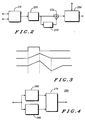
- FIG. 1 illustrates a block diagram of a radio receiver with burst detection.
- Antenna 100 receives a radio frequency signal and a radio frequency (RF) stage 110 converts the radio frequency signal to an in-phase signal (I) and a quadrature signal (Q).
- An analog to digital converter 120 samples the in-phase signal and the quadrature signal to produce a digital in-phase signal and a digital . quadrature signal in response to a sample timing from a timing circuit 130.
- a burst detector 140 establishes a coarse timing reference T 1 in response to the digital in-phase signal and the digital quadrature signal from the analog to digital converter 120 and in response to the sample time from the timing circuit 130.
- the digital in-phase signal and the digital quadrature signal from the analog to digital converter 120 are stored in a buffer 150.
- the signals stored in the buffer 150 are transferred to a receiver 160. Thereafter, the receiver provides a fine timing reference to the timing circuit 130 and can deliver received data to a voice decoder, a data unit and a call processor 170, for example, of the radio receiver.
- the present invention increases system capacity and conserves frequency spectrum by not requiring dedicated patterns to establish a timing reference. Reliable burst detection by the present invention is possible even when a transmitter and receiver obtain large frequency differences due to Doppler shifts or crystal errors. This is because the filter of the present invention reliably detects bursts without using dedicated patterns or a programmed correlation sequence. The present invention does not degrade the signal to noise ratio due to false detection of correlation peaks. In the present invention, the characteristics of the signal itself are recognized. For instance, a constant power transient characteristic can be detected when the signal bursts. The present invention also avoids multiple receiver paths to establish a timing reference, such as in a Rake receiver, thus saving processing time.
- the timing circuit 130 When the burst detector 140 detects a burst as indicated by the coarse timing reference T 1 , the timing circuit 130 causes a mode change from a burst detection mode to a gated receive mode. While in the burst detection mode, a timing reference has not yet been obtained by the burst detector 140 and information can not yet be extracted to provide an output for the user of the receiver. After a timing reference has been obtained by the burst detector 140, information can subsequently be obtained from the received signal by the receiver 160 under the assumption that the timing will be slowly varying.
- a mode switch 180 switches between the burst detection mode and the gated receive mode in response to the timing circuit 130. During the gated receive mode, slow variations in timing will be corrected by the receiver 160 via a fine timing reference. The receiver 160 generates the fine timing reference from its synchronization resulting from extracting information from the received signal to compensate for slow variations in timing.
- the timing circuit 130 provides the sample time to clock the sampling by the analog to digital converter 120 and also provides the sample time for digital circuits of the burst detector 140.
- the timing circuit 130 could contain, for example, a latch and a counter. Upon detection of the burst as indicated by the coarse timing reference T 1 , the latch will be triggered causing a mode change by the switch 180. The counter will reset and begin counting in response to the coarse timing reference T 1 to generate the sample time for clocking of the analog to digital converter 120 and the burst detector 140.
- FIG. 2 illustrates a block diagram of an embodiment of a burst detector according to the present invention.
- a signal power detector 210 detects a power magnitude P(n) of a combination of the digital in-phase signal and the digital quadrature signal.
- a digital filter 220 having a impulse response corresponding to a magnitude and duration of the expected burst filters the power magnitude P(n) and produces a signal A(n).
- a subtractor 230 subtracts a delayed version of the signal A(n), produced by a delay circuit 240, from the signal A(n) to provide the detection signal D(n).
- An edge detector 250 detects an edge of the detection signal D(n).
- the digital filter 220 filters the power magnitude P(n) to reduce the power of the noise. The result of this filtering increases the signal to noise ratio and hence improves the quality of the detector.
- the digital filter 220 could be a finite impulse response (FIR) filter having characteristics close to or approaching that of the expected burst. A digital filter 220 matched to the expected burst would provide the maximum signal to noise ratio.
- the digital filter 220 could be any filter that increases the signal to noise ratio.
- the edge detector 250 detects an edge of the detection signal D(n) and is clocked by the sample time of the timing circuit 130.
- the edge detector 250 could use thresholds to detect the edge of the detection signal D(n).
- the exemplary edge detector 250 in this embodiment uses a maximum or minimum first, second, third or fourth approach to determine a leading edge of the burst, as will be described below with reference to FIG. 4.
- the edge detector 250 can also use a fifth approach such as a pattern match approach.
- FIG. 3 illustrates a timing diagram for the burst detector illustrating signals A(n) and D(n) generated in response to an ideal square wave P(n).
- the maximum and/or minimum of the detection signal D(n) of FIG. 3 can be detected by the edge detector 250 in the below-discussed first, second or third approaches to determine the leading edge of the burst.
- the time of the signal A(n) can instead be detected in a fourth approach to determine the leading edge of the signal as will be discussed below with respect to FIG. 4.
- pattern matching of a shape of the detection signal D(n) with an expected waveform such as, for example, the shape for signal D(n) is illustrated in FIG. 3.
- FIG. 4 illustrates implementations of an edge detector using maximum and/or minimum threshold detectors 260, 280 and a timing distance detector 270.
- the edge detector 250 detects one of or both the maximum and minimum of the detection signal D(n) when using the below-described first, second and third approaches.
- the maximum threshold detector 260 and the minimum threshold detector 280 are preferably threshold detectors, any selector which identifies the maximum and minimum is appropriate.
- the time of the maximum and/or the time of the minimum can be determined by thresholding.
- the maximum threshold detector 260 thresholds the detection signal D(n) to determine if the maximum of the detection D(n) is greater than a maximum threshold.
- the minimum threshold detector 280 thresholds to determine if the detection signal D(n) is less than a minimum threshold.
- a first approach in determining the leading edge of the burst is to determine the time of the maximum and the time of the minimum of the detection signal D(n). If the difference in the time of the maximum and the time of the minimum is approximately equal to the duration of the expected bursts, the leading edge of the burst can be determined from the time of the maximum, the time of the minimum and the duration of the expected bursts.
- the maximum is determined by the maximum threshold detector 260 and the time of the minimum is determined by the minimum threshold detector 280.
- the distance between the time of the maximum and the time of the minimum is determined by the timing distance detector 270.
- the timing distance detector 270 is provided by a determining circuit connected to the maximum threshold detector 260 and the minimum threshold detector 280 to determine a leading edge of the burst based on an average of the time of the maximum and of the minimum.
- the average of the time of the maximum and of the minimum preferably is compared to one and one-half times the expected length of the bursts. Therefore, the leading edge of the bursts is based on an average of the time of the maximum and of the minimum less one and one-half times the expected length of the burst.
- a second approach would be to determine the time of the maximum of the detection signal D(n). From the time of the maximum detected by the maximum threshold detector 260 by itself and the duration of the expected burst, the leading edge of the burst can be determined. The illustrated minimum threshold detector 280 and the timing distance detector 270 are not needed in this second approach.
- a third approach would be to determine the time of the minimum of the detection signal D(n). From the time of the minimum determined by the minimum threshold detector 280 and the duration of the expected burst, the leading edge of the burst can be determined. The illustrated maximum threshold detector 260 and the timing distance detector 270 are not needed in this third approach.
- the leading edge of the burst could be determined from detecting the time of the maximum of the signal A(n). From the time of the maximum and the duration of the burst the leading edge of the burst can be determined.
- the time of the maximum can be determined by thresholding to determine if the maximum of the detection signal D(n) is greater than a maximum threshold.
- the maximum threshold detector 260 is thus connected to receive signal A(n).
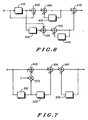
- FIG. 5 illustrates a burst detector according to an alternative embodiment of the present invention having a different configuration capable of achieving the same result of the embodiment of FIG. 2.
- the embodiment of FIG. 4 is mathematically equivalent to the embodiment of FIG. 2.
- a signal power detector 310 detects a power magnitude P(n) of a combination of the digital in-phase signal and the digital quadrature signal.
- a digital filter 320 having a impulse response corresponding to a magnitude and duration of the expected burst filters the power magnitude P(n) and produces a signal A(n).
- a delay circuit 340 delays the power magnitude P(n) and a moving average filter 360 filters the delayed power magnitude P(n).
- the moving average filter 360 also has a impulse response corresponding to a magnitude and duration of the expected burst.
- a subtractor 330 subtracts an output of the moving average filter 360 from the signal A(n) to provide the detection signal D(n).
- An edge detector 350 detects an edge of the detection signal D(n).
- the edge detector 350 of FIG. 5 is illustrated by the exemplary pattern match edge detector using a fifth approach.
- the pattern match edge detector in block 350 of FIG. 5 contains a pattern match circuit to pattern match a shape of the detection signal D(n) with an expected waveform such as the shape of, for example, the waveform illustrated for signal D(n) in the timing diagram of FIG. 3.
- the edge detector 350 can also be a maximum and/or minimum edge detector as discussed above with respect to the first, second, third and fourth approaches. Further, any arrangement for the filters and delays could use these and other edge detector approaches.
- FIG. 6 illustrates a detailed block diagram showing an alternative implementation of the filters and the delays according to the present invention.
- the moving average filters and delays of FIGS. 2 and 5, for example, can be implemented by the illustrated configurations for the delays 410, 420, 430 and 440 and by the illustrated connections therebetween of the adders and subtractors 450, 460, 470, 480 and 490.
- FIG. 7 illustrates a detailed block diagram showing another alternative implementation of the filters and the delays of FIGS. 2 and 5, for example, according to the present invention.
- Adders and subtractors 545, 550 and 560 are connected between delays 510, 520 and 530 as illustrated.
- a multiplier 570 multiplies the output of the delay 510 by a factor of two before providing an output to element 540.
Landscapes
- Computer Networks & Wireless Communication (AREA)
- Signal Processing (AREA)
- Engineering & Computer Science (AREA)
- Synchronisation In Digital Transmission Systems (AREA)
- Digital Transmission Methods That Use Modulated Carrier Waves (AREA)
- Circuits Of Receivers In General (AREA)
- Dc Digital Transmission (AREA)
- Radar Systems Or Details Thereof (AREA)
- Stabilization Of Oscillater, Synchronisation, Frequency Synthesizers (AREA)
- Protection Of Generators And Motors (AREA)
- Transmission And Conversion Of Sensor Element Output (AREA)
- Emergency Protection Circuit Devices (AREA)
- Cable Transmission Systems, Equalization Of Radio And Reduction Of Echo (AREA)
Claims (10)
- Ein Burstdetektor zur Detektion eines Bursts enthaltend:einen Filter (220) mit einer Impulsantwort -Charakteristik eines erwarteten Bursts zur Filterung eines empfangenen Signals;eine Subtrahierer (230), der wirksam an den Filter gekoppelt ist, um durch Subtrahieren einer gefilterten Version des empfangenen Signals von einer verzögerten und gefilterten Version des empfangenen Signals ein Detektionssignal bereitzustellen undein Burstflankendetektor (250), der wirksam an den Subtrahierer gekoppelt ist, um das Detektionssignal zu empfangen und die erste Flanke des Burst zu detektieren.
- Ein Burstdetektor nach Anspruch 1,bei dem der Filter durch ein Moving-Average-Filter charakterisiert ist, welches wirksam gekoppelt ist, um basierend auf dem empfangenen Signal ein Durchschnittssignal bereitzustellenwobei der Subtrahierer durch eine Verzögerungsstufe (240) charakterisiert ist, die wirksam an das Moving-Average-Filter (220) gekoppelt ist, um das Durchschnittssignal zu verzögern und ein verzögertes Durchschnittssignal bereitzustellen;und bei dem der Subtrahierer weiter durch einen Subtraktionsschaltkreis (230) charakterisiert ist, der wirksam gekoppelt ist, um das verzögerte Durchschnittssignal der Verzögerungsstufe von dem Durchschnittssignal des Moving-Average-Filter zu subtrahieren, um das Detektionssignal bereitzustellen.
- Ein Burstdetektor nach Anspruch 2,bei dem die Verzögerungsstufe eine Verzögerung aufweist, die einer Dauer des erwarteten Bursts entspricht.
- Ein Burstdetektor nach Anspruch 1,bei dem der Subtrahierer durch eine Verzögerungsstufe (340) gekennzeichnet ist, die vorgesehen ist, das empfangene Signal zu erhalten und ein verzögertes empfangenes Signal bereitzustellen;bei dem das Filter durch ein erstes Moving-Average-Filter (320) gekennzeichnet ist und vorgesehen ist, das Durchschnittsignal bereitzustellen, welches auf dem empfangenem Signal basiert und durch ein zweites Moving-Average-Filter (360) gekennzeichnet ist, welches wirksam an die Verzögerungsstufe (340) gekoppelt ist, um ein verzögertes Durchschnittssignal bereitzustellen, das auf dem verzögerten empfangenen Signal basiert undbei dem der Subtrahierer weiter durch einen Subtraktionsschaltkreis (330) gekennzeichnet ist, der wirksam gekoppelt ist, um das verzögerte Durchschnittssignal des zweiten Moving-Average-Filters von dem Durchschnittssignal des ersten Moving-Average-Filters zu subtrahieren um ein Detektionssignal bereitzustellen.
- Ein Burstdetektor nach Anspruch 1,bei dem der Burstflankendetektor durch eine Maximum-/ Minimum- Auswahleinheit (250) gekennzeichnet ist, die wirksam an den Subtrahierer gekoppelt ist, um ein Maximum oder Minimum des Detektionssignals auszuwählen.
- Ein Burstdetektor nach Anspruch 1,bei dem der Burstflankendetektor durch ein Mustervergleichsschaltkreis (350) charakterisiert ist, der wirksam an den Subtrahierer gekoppelt ist, um eine Form des Detektionssignals mit der erwarteten Wellenform zu vergleichen.
- Ein Burstdetektor nach Anspruch 1,bei dem das Filter durch ein digitales, eine Impulsantwort aufweisendes Filter gekennzeichnet ist, die der Größenordnung und Dauer des erwarteten Bursts entspricht.
- Ein Verfahren zur Detektion eines Bursts enthaltend die Schritte:(a) Subtrahieren (230) einer gefilterten Version eines empfangenen Signals von einer verzögerten und gefilterten Version des empfangenen Signals, wobei das empfangene Signal durch ein Filter gefiltert wird (220), das eine Impulsantwortcharakteristik des erwarteten Burst aufweist; und(b) Detektieren (250) der ersten Flanke des Bursts als Resultat von Schritt (a).
- Ein Verfahren zur Detektion eines Burst nach Anspruch 8, bei dem Schritt (a) gekennzeichnet ist, durch die Unterschritte:(a1) Moving-Average-Filterung (220), um ein Durchschnittsignal bereitzustellen, welches auf dem empfangenen Signal basiert;(a2) Verzögern des Durchschnittsignals (240) von Schritt (a1) um ein verzögertes Durchschnittsignal bereitzustellen; und(a3) Subtrahieren (230) des verzögerten Durchschnittsignals von Schritt (a2) von dem Durchschnittsignal von Schritt (a1).
- Ein Verfahren zur Detektion eines Burst nach Anspruch 8, bei dem Schritt (a) gekennzeichnet ist, durch folgende Unterschritte:(a1) Verzögern (340) des empfangenen Signals, um ein verzögertes empfangenes Signal bereitzustellen;(a2) Moving-Average-Filterung (320) des empfangenen Signals um ein Durchschnittssignal bereitzustellen;(a3) Moving-Average-Filterung (360) des verzögerten Signals um ein verzögertes Durchschnittssignal bereit zu stellen, welches auf dem verzögerten empfangenen Signal basiert; und(a4) Subtrahieren (330) des verzögerten Durchschnittssignals von dem Durchschnittssignal.
Applications Claiming Priority (2)
| Application Number | Priority Date | Filing Date | Title |
|---|---|---|---|
| US332159 | 1994-10-31 | ||
| US08/332,159 US5621766A (en) | 1994-10-31 | 1994-10-31 | Method and apparatus for burst detecting |
Publications (3)
| Publication Number | Publication Date |
|---|---|
| EP0709975A2 EP0709975A2 (de) | 1996-05-01 |
| EP0709975A3 EP0709975A3 (de) | 2000-07-12 |
| EP0709975B1 true EP0709975B1 (de) | 2002-03-06 |
Family
ID=23296970
Family Applications (1)
| Application Number | Title | Priority Date | Filing Date |
|---|---|---|---|
| EP95116694A Expired - Lifetime EP0709975B1 (de) | 1994-10-31 | 1995-10-23 | Verfahren und Gerät zur Burst-Detektion |
Country Status (10)
| Country | Link |
|---|---|
| US (1) | US5621766A (de) |
| EP (1) | EP0709975B1 (de) |
| JP (1) | JP3268382B2 (de) |
| AT (1) | ATE214212T1 (de) |
| BR (1) | BR9505032A (de) |
| CA (1) | CA2160431C (de) |
| DE (1) | DE69525708T2 (de) |
| MX (1) | MX9504578A (de) |
| RU (1) | RU2108681C1 (de) |
| UA (1) | UA39202C2 (de) |
Families Citing this family (22)
| Publication number | Priority date | Publication date | Assignee | Title |
|---|---|---|---|---|
| US5748680A (en) * | 1994-12-16 | 1998-05-05 | Lucent Technologies Inc. | Coarse frequency burst detector for a wireline communications system |
| FI956360L (fi) * | 1995-12-29 | 1997-06-30 | Nokia Telecommunications Oy | Menetelmä yhteydenmuodostuspurskeen havaitsemiseksi ja vastaanotin |
| KR100193837B1 (ko) * | 1996-08-24 | 1999-06-15 | 윤종용 | 시분할다윈접속 디지탈 이동통신 시스템의 주파수 교정 버스트 검출방법 |
| US5864585A (en) | 1996-10-07 | 1999-01-26 | Erisman; David | Cosine segment communications system |
| US5963594A (en) * | 1996-12-31 | 1999-10-05 | Lucent Technologies Inc. | Vector tracking filter |
| JP3885909B2 (ja) * | 1997-07-25 | 2007-02-28 | ソニー株式会社 | 電力検出装置 |
| DE69908516T2 (de) * | 1998-02-14 | 2003-12-11 | Samsung Electronics Co., Ltd. | Daten kommunikationsgerät und verfahren für mobile kommunikationsanordnung mit zugeteiltem kontrollkanal |
| US7076003B1 (en) * | 1999-03-03 | 2006-07-11 | Agere Systems Inc. | Constellation design for modem receiver |
| US6480555B1 (en) * | 1999-09-02 | 2002-11-12 | Motorola, Inc. | Method and apparatus for extended range frequency correction burst detection |
| US6411914B1 (en) | 1999-11-29 | 2002-06-25 | Goodrich Corporation | System and method for coherent signal detection using wavelet functions |
| US6694469B1 (en) * | 2000-04-14 | 2004-02-17 | Qualcomm Incorporated | Method and an apparatus for a quick retransmission of signals in a communication system |
| US6993100B2 (en) * | 2000-12-12 | 2006-01-31 | Skyworks Solutions, Inc. | Burst detector |
| US7106711B2 (en) * | 2001-06-06 | 2006-09-12 | Motorola, Inc. | Method and apparatus for reducing the impact of cell reselection of GPRS/EDGE data rates |
| KR100406659B1 (ko) | 2001-11-09 | 2003-11-21 | 삼성전자주식회사 | 톤 신호의 에너지 검출 장치 및 방법 |
| WO2004095057A1 (ja) * | 2003-04-24 | 2004-11-04 | Fujitsu Limited | レーダ装置 |
| GB0407587D0 (en) * | 2004-04-02 | 2004-05-05 | Univ Nottingham Trent | Cancer associated antigens |
| US7593482B2 (en) * | 2004-09-30 | 2009-09-22 | St-Ericsson Sa | Wireless communication system with hardware-based frequency burst detection |
| US7567637B2 (en) * | 2004-09-30 | 2009-07-28 | St-Ericsson Sa | Wireless communication system and method with frequency burst acquisition feature using autocorrelation and narrowband interference detection |
| US8054918B2 (en) * | 2004-09-30 | 2011-11-08 | ST-Ericsson S.A. | Wireless communication system and method with frequency burst acquisition feature using autocorrelation |
| US7414560B2 (en) * | 2005-06-29 | 2008-08-19 | Shaojie Chen | Wireless communication system including an audio underflow protection mechanism operative with time domain isolation |
| FR2895200B1 (fr) * | 2005-12-20 | 2008-02-22 | Silicon Lab Inc | Procede d'acquisition d'un burst de correction de frequence par un dispositif de radiocommunication, et dispositif de radiocommunication correspondant. |
| JP5386943B2 (ja) * | 2008-11-20 | 2014-01-15 | 富士通株式会社 | 波形制御装置,応答素子モジュール,光スイッチ装置および光スイッチ装置の制御方法 |
Family Cites Families (7)
| Publication number | Priority date | Publication date | Assignee | Title |
|---|---|---|---|---|
| US4466108A (en) * | 1981-10-06 | 1984-08-14 | Communications Satellite Corporation | TDMA/PSK Carrier synchronization without preamble |
| US4873683A (en) * | 1987-12-04 | 1989-10-10 | Motorola, Inc. | TDMA radio system employing BPSK synchronization for QPSK signals subject to random phase variation and multipath fading |
| US5272446A (en) * | 1991-11-29 | 1993-12-21 | Comsat | Digitally implemented fast frequency estimator/demodulator for low bit rate maritime and mobile data communications without the use of an acquisition preamble |
| US5276706A (en) * | 1992-05-20 | 1994-01-04 | Hughes Aircraft Company | System and method for minimizing frequency offsets between digital communication stations |
| US5282227A (en) * | 1992-05-21 | 1994-01-25 | The Titan Corporation | Communication signal detection and acquisition |
| FI93068C (fi) * | 1992-07-27 | 1995-02-10 | Nokia Mobile Phones Ltd | Kytkentä häiriöiden haittavaikutusten pienentämiseksi sovitettua suodatinta käyttävissä vastaanottimissa |
| JP2720721B2 (ja) * | 1992-08-21 | 1998-03-04 | 日本電気株式会社 | 変復調装置 |
-
1994
- 1994-10-31 US US08/332,159 patent/US5621766A/en not_active Expired - Lifetime
-
1995
- 1995-10-12 CA CA002160431A patent/CA2160431C/en not_active Expired - Fee Related
- 1995-10-23 EP EP95116694A patent/EP0709975B1/de not_active Expired - Lifetime
- 1995-10-23 DE DE69525708T patent/DE69525708T2/de not_active Expired - Fee Related
- 1995-10-23 AT AT95116694T patent/ATE214212T1/de not_active IP Right Cessation
- 1995-10-30 UA UA95104724A patent/UA39202C2/uk unknown
- 1995-10-30 RU RU95118724A patent/RU2108681C1/ru not_active IP Right Cessation
- 1995-10-30 JP JP30339795A patent/JP3268382B2/ja not_active Expired - Fee Related
- 1995-10-31 MX MX9504578A patent/MX9504578A/es unknown
- 1995-10-31 BR BR9505032A patent/BR9505032A/pt not_active IP Right Cessation
Also Published As
| Publication number | Publication date |
|---|---|
| CA2160431A1 (en) | 1996-05-01 |
| US5621766A (en) | 1997-04-15 |
| EP0709975A2 (de) | 1996-05-01 |
| BR9505032A (pt) | 1997-10-21 |
| CA2160431C (en) | 2000-02-22 |
| JPH0927802A (ja) | 1997-01-28 |
| JP3268382B2 (ja) | 2002-03-25 |
| EP0709975A3 (de) | 2000-07-12 |
| ATE214212T1 (de) | 2002-03-15 |
| UA39202C2 (uk) | 2001-06-15 |
| MX9504578A (es) | 1997-06-28 |
| RU2108681C1 (ru) | 1998-04-10 |
| DE69525708D1 (de) | 2002-04-11 |
| DE69525708T2 (de) | 2002-08-01 |
Similar Documents
| Publication | Publication Date | Title |
|---|---|---|
| EP0709975B1 (de) | Verfahren und Gerät zur Burst-Detektion | |
| US4587662A (en) | TDMA spread-spectrum receiver with coherent detection | |
| US5748681A (en) | Offset correction for a homodyne radio | |
| EP0307950B1 (de) | Kreuzpolarisationsinterferenzkompensator | |
| US6480555B1 (en) | Method and apparatus for extended range frequency correction burst detection | |
| JP2751840B2 (ja) | 信号検出装置 | |
| US5291081A (en) | Apparatus for detection of non-modulated signal and frequency acquisition | |
| WO1996008085A3 (en) | Rfi suppression circuit and method | |
| GB2300093A (en) | Receiver for timing recovery and frequency estimation | |
| EP1683316B1 (de) | Vorrichtung zur bestimmung eines frequenzoffsetfehlers und darauf basierender empfänger | |
| US6032048A (en) | Method and apparatus for compensating for click noise in an FM receiver | |
| US8254437B2 (en) | Transmitting apparatus, receiving apparatus and communication system | |
| CA2048933A1 (en) | Carrier aquisition apparatus for digital satellite communication system | |
| US6341146B1 (en) | Phase-shift-keying demodulator and demodulation method using a period-width windowing technique | |
| US4241312A (en) | Self-calibrating threshold detector | |
| US5539783A (en) | Non-coherent synchronization signal detector | |
| US5206887A (en) | Unique word detection apparatus | |
| WO1996013897A1 (en) | Communication device with reduced sensitivity to in-channel interference | |
| EP0506708B1 (de) | Verfahren und gerät zur statistischen fm-rauschunterdrückung | |
| EP1069554A1 (de) | Jittearmersleistungsdetektor für Zeitmultiplex-Vielfachzugriffsübertragung | |
| JPH1023081A (ja) | 信号検出回路 | |
| KR100288200B1 (ko) | 이동통신시스템의동기형복조장치및방법 | |
| JP2655080B2 (ja) | スペクトラム拡散無線通信方式の受信装置 | |
| KR0136371Y1 (ko) | 데이타 슬라이서 | |
| KR20000034473A (ko) | 코드 분할 다중 접속 시스템의 간섭신호 제거회로 |
Legal Events
| Date | Code | Title | Description |
|---|---|---|---|
| PUAI | Public reference made under article 153(3) epc to a published international application that has entered the european phase |
Free format text: ORIGINAL CODE: 0009012 |
|
| AK | Designated contracting states |
Kind code of ref document: A2 Designated state(s): AT BE CH DE DK ES FR GB GR IE IT LI LU MC NL PT SE |
|
| PUAL | Search report despatched |
Free format text: ORIGINAL CODE: 0009013 |
|
| AK | Designated contracting states |
Kind code of ref document: A3 Designated state(s): AT BE CH DE DK ES FR GB GR IE IT LI LU MC NL PT SE |
|
| RIC1 | Information provided on ipc code assigned before grant |
Free format text: 7H 04B 7/212 A, 7H 04B 7/26 B |
|
| 17P | Request for examination filed |
Effective date: 20010112 |
|
| GRAG | Despatch of communication of intention to grant |
Free format text: ORIGINAL CODE: EPIDOS AGRA |
|
| GRAG | Despatch of communication of intention to grant |
Free format text: ORIGINAL CODE: EPIDOS AGRA |
|
| GRAH | Despatch of communication of intention to grant a patent |
Free format text: ORIGINAL CODE: EPIDOS IGRA |
|
| 17Q | First examination report despatched |
Effective date: 20010409 |
|
| GRAH | Despatch of communication of intention to grant a patent |
Free format text: ORIGINAL CODE: EPIDOS IGRA |
|
| REG | Reference to a national code |
Ref country code: GB Ref legal event code: IF02 |
|
| GRAA | (expected) grant |
Free format text: ORIGINAL CODE: 0009210 |
|
| AK | Designated contracting states |
Kind code of ref document: B1 Designated state(s): AT BE CH DE DK ES FR GB GR IE IT LI LU MC NL PT SE |
|
| PG25 | Lapsed in a contracting state [announced via postgrant information from national office to epo] |
Ref country code: NL Free format text: LAPSE BECAUSE OF FAILURE TO SUBMIT A TRANSLATION OF THE DESCRIPTION OR TO PAY THE FEE WITHIN THE PRESCRIBED TIME-LIMIT Effective date: 20020306 Ref country code: LI Free format text: LAPSE BECAUSE OF FAILURE TO SUBMIT A TRANSLATION OF THE DESCRIPTION OR TO PAY THE FEE WITHIN THE PRESCRIBED TIME-LIMIT Effective date: 20020306 Ref country code: IT Free format text: LAPSE BECAUSE OF FAILURE TO SUBMIT A TRANSLATION OF THE DESCRIPTION OR TO PAY THE FEE WITHIN THE PRESCRIBED TIME-LIMIT;WARNING: LAPSES OF ITALIAN PATENTS WITH EFFECTIVE DATE BEFORE 2007 MAY HAVE OCCURRED AT ANY TIME BEFORE 2007. THE CORRECT EFFECTIVE DATE MAY BE DIFFERENT FROM THE ONE RECORDED. Effective date: 20020306 Ref country code: GR Free format text: LAPSE BECAUSE OF FAILURE TO SUBMIT A TRANSLATION OF THE DESCRIPTION OR TO PAY THE FEE WITHIN THE PRESCRIBED TIME-LIMIT Effective date: 20020306 Ref country code: FR Free format text: LAPSE BECAUSE OF FAILURE TO SUBMIT A TRANSLATION OF THE DESCRIPTION OR TO PAY THE FEE WITHIN THE PRESCRIBED TIME-LIMIT Effective date: 20020306 Ref country code: CH Free format text: LAPSE BECAUSE OF FAILURE TO SUBMIT A TRANSLATION OF THE DESCRIPTION OR TO PAY THE FEE WITHIN THE PRESCRIBED TIME-LIMIT Effective date: 20020306 Ref country code: BE Free format text: LAPSE BECAUSE OF FAILURE TO SUBMIT A TRANSLATION OF THE DESCRIPTION OR TO PAY THE FEE WITHIN THE PRESCRIBED TIME-LIMIT Effective date: 20020306 Ref country code: AT Free format text: LAPSE BECAUSE OF FAILURE TO SUBMIT A TRANSLATION OF THE DESCRIPTION OR TO PAY THE FEE WITHIN THE PRESCRIBED TIME-LIMIT Effective date: 20020306 |
|
| REF | Corresponds to: |
Ref document number: 214212 Country of ref document: AT Date of ref document: 20020315 Kind code of ref document: T |
|
| REG | Reference to a national code |
Ref country code: CH Ref legal event code: EP |
|
| REF | Corresponds to: |
Ref document number: 69525708 Country of ref document: DE Date of ref document: 20020411 |
|
| PG25 | Lapsed in a contracting state [announced via postgrant information from national office to epo] |
Ref country code: SE Free format text: LAPSE BECAUSE OF FAILURE TO SUBMIT A TRANSLATION OF THE DESCRIPTION OR TO PAY THE FEE WITHIN THE PRESCRIBED TIME-LIMIT Effective date: 20020606 Ref country code: PT Free format text: LAPSE BECAUSE OF FAILURE TO SUBMIT A TRANSLATION OF THE DESCRIPTION OR TO PAY THE FEE WITHIN THE PRESCRIBED TIME-LIMIT Effective date: 20020606 Ref country code: DK Free format text: LAPSE BECAUSE OF FAILURE TO SUBMIT A TRANSLATION OF THE DESCRIPTION OR TO PAY THE FEE WITHIN THE PRESCRIBED TIME-LIMIT Effective date: 20020606 |
|
| NLV1 | Nl: lapsed or annulled due to failure to fulfill the requirements of art. 29p and 29m of the patents act | ||
| REG | Reference to a national code |
Ref country code: CH Ref legal event code: PL |
|
| PG25 | Lapsed in a contracting state [announced via postgrant information from national office to epo] |
Ref country code: ES Free format text: LAPSE BECAUSE OF FAILURE TO SUBMIT A TRANSLATION OF THE DESCRIPTION OR TO PAY THE FEE WITHIN THE PRESCRIBED TIME-LIMIT Effective date: 20020925 |
|
| PG25 | Lapsed in a contracting state [announced via postgrant information from national office to epo] |
Ref country code: LU Free format text: LAPSE BECAUSE OF NON-PAYMENT OF DUE FEES Effective date: 20021023 Ref country code: IE Free format text: LAPSE BECAUSE OF NON-PAYMENT OF DUE FEES Effective date: 20021023 |
|
| EN | Fr: translation not filed | ||
| PLBE | No opposition filed within time limit |
Free format text: ORIGINAL CODE: 0009261 |
|
| STAA | Information on the status of an ep patent application or granted ep patent |
Free format text: STATUS: NO OPPOSITION FILED WITHIN TIME LIMIT |
|
| 26N | No opposition filed |
Effective date: 20021209 |
|
| PG25 | Lapsed in a contracting state [announced via postgrant information from national office to epo] |
Ref country code: MC Free format text: LAPSE BECAUSE OF NON-PAYMENT OF DUE FEES Effective date: 20030501 |
|
| REG | Reference to a national code |
Ref country code: IE Ref legal event code: MM4A |
|
| PGFP | Annual fee paid to national office [announced via postgrant information from national office to epo] |
Ref country code: GB Payment date: 20030915 Year of fee payment: 9 |
|
| PG25 | Lapsed in a contracting state [announced via postgrant information from national office to epo] |
Ref country code: GB Free format text: LAPSE BECAUSE OF NON-PAYMENT OF DUE FEES Effective date: 20041023 |
|
| GBPC | Gb: european patent ceased through non-payment of renewal fee |
Effective date: 20041023 |
|
| PGFP | Annual fee paid to national office [announced via postgrant information from national office to epo] |
Ref country code: DE Payment date: 20061031 Year of fee payment: 12 |
|
| PG25 | Lapsed in a contracting state [announced via postgrant information from national office to epo] |
Ref country code: DE Free format text: LAPSE BECAUSE OF NON-PAYMENT OF DUE FEES Effective date: 20080501 |
|
| P01 | Opt-out of the competence of the unified patent court (upc) registered |
Effective date: 20230520 |