EP0710060B1 - Verfahren zur Herstellung von Kunststoffkartenträgern, Anordnung zur Durchführung des Verfahrens und Anwendung des Verfahrens für die Produktion von Mikroschaltungskarten - Google Patents
Verfahren zur Herstellung von Kunststoffkartenträgern, Anordnung zur Durchführung des Verfahrens und Anwendung des Verfahrens für die Produktion von Mikroschaltungskarten Download PDFInfo
- Publication number
- EP0710060B1 EP0710060B1 EP94402443A EP94402443A EP0710060B1 EP 0710060 B1 EP0710060 B1 EP 0710060B1 EP 94402443 A EP94402443 A EP 94402443A EP 94402443 A EP94402443 A EP 94402443A EP 0710060 B1 EP0710060 B1 EP 0710060B1
- Authority
- EP
- European Patent Office
- Prior art keywords
- printing
- roller
- strip
- speed
- cutting
- Prior art date
- Legal status (The legal status is an assumption and is not a legal conclusion. Google has not performed a legal analysis and makes no representation as to the accuracy of the status listed.)
- Expired - Lifetime
Links
- 238000000034 method Methods 0.000 title claims description 31
- 238000004519 manufacturing process Methods 0.000 title claims description 30
- 239000004033 plastic Substances 0.000 title claims description 22
- 238000007639 printing Methods 0.000 claims description 61
- 238000005520 cutting process Methods 0.000 claims description 27
- 238000001035 drying Methods 0.000 claims description 6
- 238000010030 laminating Methods 0.000 claims description 5
- 238000001514 detection method Methods 0.000 claims description 4
- 238000010981 drying operation Methods 0.000 claims description 4
- 238000000151 deposition Methods 0.000 claims description 3
- 238000003780 insertion Methods 0.000 claims description 3
- 239000004065 semiconductor Substances 0.000 claims description 3
- 239000002966 varnish Substances 0.000 claims description 3
- 238000006073 displacement reaction Methods 0.000 claims description 2
- 230000001105 regulatory effect Effects 0.000 claims description 2
- 239000000463 material Substances 0.000 claims 3
- 238000003475 lamination Methods 0.000 claims 2
- 230000001681 protective effect Effects 0.000 claims 1
- 239000010410 layer Substances 0.000 description 9
- 239000011159 matrix material Substances 0.000 description 3
- 238000005096 rolling process Methods 0.000 description 3
- 239000003086 colorant Substances 0.000 description 2
- 230000037431 insertion Effects 0.000 description 2
- 238000009434 installation Methods 0.000 description 2
- 238000003801 milling Methods 0.000 description 2
- 239000011241 protective layer Substances 0.000 description 2
- 239000002356 single layer Substances 0.000 description 2
- 238000000429 assembly Methods 0.000 description 1
- 230000000712 assembly Effects 0.000 description 1
- YFXPPSKYMBTNAV-UHFFFAOYSA-N bensultap Chemical compound C=1C=CC=CC=1S(=O)(=O)SCC(N(C)C)CSS(=O)(=O)C1=CC=CC=C1 YFXPPSKYMBTNAV-UHFFFAOYSA-N 0.000 description 1
- 239000011248 coating agent Substances 0.000 description 1
- 238000000576 coating method Methods 0.000 description 1
- 210000002816 gill Anatomy 0.000 description 1
- 239000007788 liquid Substances 0.000 description 1
- 238000007645 offset printing Methods 0.000 description 1
- 230000001012 protector Effects 0.000 description 1
- 230000005855 radiation Effects 0.000 description 1
- 238000011084 recovery Methods 0.000 description 1
- 238000002791 soaking Methods 0.000 description 1
- 238000003860 storage Methods 0.000 description 1
- 238000002604 ultrasonography Methods 0.000 description 1
- 238000011144 upstream manufacturing Methods 0.000 description 1
- 238000009736 wetting Methods 0.000 description 1
- 239000000080 wetting agent Substances 0.000 description 1
Images


Classifications
-
- H—ELECTRICITY
- H05—ELECTRIC TECHNIQUES NOT OTHERWISE PROVIDED FOR
- H05K—PRINTED CIRCUITS; CASINGS OR CONSTRUCTIONAL DETAILS OF ELECTRIC APPARATUS; MANUFACTURE OF ASSEMBLAGES OF ELECTRICAL COMPONENTS
- H05K3/00—Apparatus or processes for manufacturing printed circuits
- H05K3/10—Apparatus or processes for manufacturing printed circuits in which conductive material is applied to the insulating support in such a manner as to form the desired conductive pattern
- H05K3/12—Apparatus or processes for manufacturing printed circuits in which conductive material is applied to the insulating support in such a manner as to form the desired conductive pattern using thick film techniques, e.g. printing techniques to apply the conductive material or similar techniques for applying conductive paste or ink patterns
- H05K3/1275—Apparatus or processes for manufacturing printed circuits in which conductive material is applied to the insulating support in such a manner as to form the desired conductive pattern using thick film techniques, e.g. printing techniques to apply the conductive material or similar techniques for applying conductive paste or ink patterns by other printing techniques, e.g. letterpress printing, intaglio printing, lithographic printing, offset printing
-
- H—ELECTRICITY
- H05—ELECTRIC TECHNIQUES NOT OTHERWISE PROVIDED FOR
- H05K—PRINTED CIRCUITS; CASINGS OR CONSTRUCTIONAL DETAILS OF ELECTRIC APPARATUS; MANUFACTURE OF ASSEMBLAGES OF ELECTRICAL COMPONENTS
- H05K3/00—Apparatus or processes for manufacturing printed circuits
- H05K3/0097—Processing two or more printed circuits simultaneously, e.g. made from a common substrate, or temporarily stacked circuit boards
-
- H—ELECTRICITY
- H05—ELECTRIC TECHNIQUES NOT OTHERWISE PROVIDED FOR
- H05K—PRINTED CIRCUITS; CASINGS OR CONSTRUCTIONAL DETAILS OF ELECTRIC APPARATUS; MANUFACTURE OF ASSEMBLAGES OF ELECTRICAL COMPONENTS
- H05K1/00—Printed circuits
- H05K1/02—Details
- H05K1/0266—Marks, test patterns or identification means
- H05K1/0269—Marks, test patterns or identification means for visual or optical inspection
-
- H—ELECTRICITY
- H05—ELECTRIC TECHNIQUES NOT OTHERWISE PROVIDED FOR
- H05K—PRINTED CIRCUITS; CASINGS OR CONSTRUCTIONAL DETAILS OF ELECTRIC APPARATUS; MANUFACTURE OF ASSEMBLAGES OF ELECTRICAL COMPONENTS
- H05K1/00—Printed circuits
- H05K1/02—Details
- H05K1/03—Use of materials for the substrate
- H05K1/0393—Flexible materials
-
- H—ELECTRICITY
- H05—ELECTRIC TECHNIQUES NOT OTHERWISE PROVIDED FOR
- H05K—PRINTED CIRCUITS; CASINGS OR CONSTRUCTIONAL DETAILS OF ELECTRIC APPARATUS; MANUFACTURE OF ASSEMBLAGES OF ELECTRICAL COMPONENTS
- H05K1/00—Printed circuits
- H05K1/02—Details
- H05K1/09—Use of materials for the conductive, e.g. metallic pattern
- H05K1/092—Dispersed materials, e.g. conductive pastes or inks
- H05K1/095—Dispersed materials, e.g. conductive pastes or inks for polymer thick films, i.e. having a permanent organic polymeric binder
-
- H—ELECTRICITY
- H05—ELECTRIC TECHNIQUES NOT OTHERWISE PROVIDED FOR
- H05K—PRINTED CIRCUITS; CASINGS OR CONSTRUCTIONAL DETAILS OF ELECTRIC APPARATUS; MANUFACTURE OF ASSEMBLAGES OF ELECTRICAL COMPONENTS
- H05K2201/00—Indexing scheme relating to printed circuits covered by H05K1/00
- H05K2201/09—Shape and layout
- H05K2201/09818—Shape or layout details not covered by a single group of H05K2201/09009 - H05K2201/09809
- H05K2201/09918—Optically detected marks used for aligning tool relative to the PCB, e.g. for mounting of components
-
- H—ELECTRICITY
- H05—ELECTRIC TECHNIQUES NOT OTHERWISE PROVIDED FOR
- H05K—PRINTED CIRCUITS; CASINGS OR CONSTRUCTIONAL DETAILS OF ELECTRIC APPARATUS; MANUFACTURE OF ASSEMBLAGES OF ELECTRICAL COMPONENTS
- H05K2203/00—Indexing scheme relating to apparatus or processes for manufacturing printed circuits covered by H05K3/00
- H05K2203/01—Tools for processing; Objects used during processing
- H05K2203/0104—Tools for processing; Objects used during processing for patterning or coating
- H05K2203/0113—Female die used for patterning or transferring, e.g. temporary substrate having recessed pattern
-
- H—ELECTRICITY
- H05—ELECTRIC TECHNIQUES NOT OTHERWISE PROVIDED FOR
- H05K—PRINTED CIRCUITS; CASINGS OR CONSTRUCTIONAL DETAILS OF ELECTRIC APPARATUS; MANUFACTURE OF ASSEMBLAGES OF ELECTRICAL COMPONENTS
- H05K2203/00—Indexing scheme relating to apparatus or processes for manufacturing printed circuits covered by H05K3/00
- H05K2203/01—Tools for processing; Objects used during processing
- H05K2203/0104—Tools for processing; Objects used during processing for patterning or coating
- H05K2203/0143—Using a roller; Specific shape thereof; Providing locally adhesive portions thereon
-
- H—ELECTRICITY
- H05—ELECTRIC TECHNIQUES NOT OTHERWISE PROVIDED FOR
- H05K—PRINTED CIRCUITS; CASINGS OR CONSTRUCTIONAL DETAILS OF ELECTRIC APPARATUS; MANUFACTURE OF ASSEMBLAGES OF ELECTRICAL COMPONENTS
- H05K2203/00—Indexing scheme relating to apparatus or processes for manufacturing printed circuits covered by H05K3/00
- H05K2203/05—Patterning and lithography; Masks; Details of resist
- H05K2203/0502—Patterning and lithography
- H05K2203/0534—Offset printing, i.e. transfer of a pattern from a carrier onto the substrate by using an intermediate member
-
- H—ELECTRICITY
- H05—ELECTRIC TECHNIQUES NOT OTHERWISE PROVIDED FOR
- H05K—PRINTED CIRCUITS; CASINGS OR CONSTRUCTIONAL DETAILS OF ELECTRIC APPARATUS; MANUFACTURE OF ASSEMBLAGES OF ELECTRICAL COMPONENTS
- H05K2203/00—Indexing scheme relating to apparatus or processes for manufacturing printed circuits covered by H05K3/00
- H05K2203/15—Position of the PCB during processing
- H05K2203/1545—Continuous processing, i.e. involving rolls moving a band-like or solid carrier along a continuous production path
-
- H—ELECTRICITY
- H05—ELECTRIC TECHNIQUES NOT OTHERWISE PROVIDED FOR
- H05K—PRINTED CIRCUITS; CASINGS OR CONSTRUCTIONAL DETAILS OF ELECTRIC APPARATUS; MANUFACTURE OF ASSEMBLAGES OF ELECTRICAL COMPONENTS
- H05K2203/00—Indexing scheme relating to apparatus or processes for manufacturing printed circuits covered by H05K3/00
- H05K2203/15—Position of the PCB during processing
- H05K2203/1572—Processing both sides of a PCB by the same process; Providing a similar arrangement of components on both sides; Making interlayer connections from two sides
-
- H—ELECTRICITY
- H05—ELECTRIC TECHNIQUES NOT OTHERWISE PROVIDED FOR
- H05K—PRINTED CIRCUITS; CASINGS OR CONSTRUCTIONAL DETAILS OF ELECTRIC APPARATUS; MANUFACTURE OF ASSEMBLAGES OF ELECTRICAL COMPONENTS
- H05K3/00—Apparatus or processes for manufacturing printed circuits
- H05K3/0011—Working of insulating substrates or insulating layers
- H05K3/0044—Mechanical working of the substrate, e.g. drilling or punching
- H05K3/0052—Depaneling, i.e. dividing a panel into circuit boards; Working of the edges of circuit boards
-
- H—ELECTRICITY
- H05—ELECTRIC TECHNIQUES NOT OTHERWISE PROVIDED FOR
- H05K—PRINTED CIRCUITS; CASINGS OR CONSTRUCTIONAL DETAILS OF ELECTRIC APPARATUS; MANUFACTURE OF ASSEMBLAGES OF ELECTRICAL COMPONENTS
- H05K3/00—Apparatus or processes for manufacturing printed circuits
- H05K3/22—Secondary treatment of printed circuits
- H05K3/227—Drying of printed circuits
Definitions
- the present invention relates to a method of manufacture of cards with plastic support, the device allowing the implementation of the method as well as the use of the process for the manufacture of cards micro circuits.
- the cards are made from large plates on which a plurality of cards are printed by a process offset printing then each plate is cut into strips and the strips are then cut to form plastic supports having the dimensions of a card.
- the cards are formed in multilayers from three ribbons of which a first constitutes the base layer, a other the central layer with cutouts regularly spaced for placement of the integrated chip and a third ribbon constituting the upper layer which also has regular cutouts spaced to allow the installation of the module contact.
- the three layers once assembled are then cut to the dimensions of a card.
- This process has the disadvantage of being complex in terms of assembling the different layers to form the plastic support and requires printing beforehand, either on the layer either on the top layer or on both layers at the same time patterns to be included on the menu.
- This process poses the problem of the coincidence of patterns in the case of double-sided printing. In addition it does not allow production rates to be obtained high.
- a first object of the invention is therefore to propose a process for manufacturing plastic support for semiconductor cards which allows manufacture of supports requiring a minimum take-back and transport operations from one post to the other which removes the problem of coincidence of patterns and which also allows rates of high manufacturing.
- the process includes a drying operation.
- the operation of drying is obtained by two ultraviolet tubes arranged on either side of the strip for a double sided printing.
- the method of manufacturing the plastic support involves a step of coating with varnish to protect the print before the ultraviolet drying step.
- the method of manufacture of the plastic support comprises a step of depositing a protective layer on each printed sides.
- Another object of the invention is to propose a manufacturing device allowing the implementation of the process.
- each station printing device has at least one printing device formed of an inking roller driving a plate roller in contact with a blanket, the inking roller cooperating with a film laminating roller ink on the ink roller depending on the relative speed of the inking roller and the rolling, each roll having a corresponding width approximately one of the dimensions of the map, the blanket roller being in contact with one side of the bandaged.
- each station print has on each side of the strip a printing device consisting of an inking roller driving a plate roller in contact with a blanket, the inking roller cooperating with a roller laminating the ink film on the roller ink based on relative roller speeds inking and laminating roller, each roller having a width approximately corresponding to one of the card dimensions, the two blanket rolls each side of the strip being in contact therewith.
- the press has a punch die assembly, the punch mounted on columns is driven in displacement by a system eccentric crank rod, the band being driven by an assembly formed by a driving roller and a roller presser so as to bring the printed mark opposite of a photoelectric cell arranged in the matrix.
- the training of the strip is provided by two rollers, at least one of which is knurled on both ends over a distance corresponding to the margin separating the edge of the strip from edge of the cut delimiting the card.
- the station printing operates at a speed of less than 20m / s.
- the press of cutting operates at a rate between 7000 and 13,000 cards per hour.
- Another object of the invention is to propose the use of the process for manufacturing micro-circuit cards.
- the process includes a camera counting step and a trays.
- Figure 1 shows the device part forming the impression on the plastic support in the process for manufacturing plastic supports which is used in Figure 3 in association with a chain insertion of modules.
- the printing device of figure 1 is consisting of a roller (1) supporting a strip (13) in PVC of the desired thickness for the plastic support a map and width corresponding to the dimensions in width or length of a map.
- This roller (1) delivers its ribbon (13) in a device (2) for straightening the strip so as to remove the residual curvature that this could keep after storage in roller.
- the strip (13) then passes through a set of printing stations (4a, 4b, 4c, 4d) associated in the case where printing is done on two sides with posts opposite located respectively (3a, 3b, 3c, 3d).
- Each printing station consists of a inkwell (42), respectively (32), associated with a roller ink rolling (43), respectively (33), and to a ink roller (41), respectively (31).
- the roller ink entering the inkwell becomes covered with ink and the rolling roller (43 or 33) allows by adjustment of its speed to determine the thickness of the film uniformly distributed on the ink roller (41), respectively (31).
- This ink roller cooperates with a plate roller (45), respectively (35) which carries the plates on which the patterns to be printed were engraved.
- the patterns to be printed correspond to the patterns to appear on each side of the card in the color corresponding to the printing station.
- a wetting device (44), respectively (34) consisting of two rollers (441, 442), respectively (341, 342) soaking in a tank filled with liquid wetting agent and one of which (442), respectively (342) is in contact with the inking roller (41), respectively (31).
- the pattern is transferred to the PVC tape (13) using a blanket roller (46) and respectively (36), for the printing device on the underside.
- a blanket roller (46) and respectively (36) for the printing device on the underside.
- each print station will only have the device corresponding to the side to be printed and on the opposite side without pattern we will use simply a back pressure roller.
- the whole printing device is shown with four stations so as to show the different basic colors allowing the printing of different different color patterns.
- At least one station printing at least one of the plate rollers includes in addition to the pattern to be printed the engraving of a printed mark which identifies the position of the pattern forming the card.
- the printed ribbon (13) is subjected to a drying operation carried out using two lamps ultraviolet radiation (51), one (51R) for the face front, the other (51V) for the back side of the strip (13) in case there is a double sided printing. Yes printing is done simply on the front side, only the UV lamp (51R) will be used.
- the drying device is followed by a set of four rollers, two (52, 53) cooperating with the strip by friction to drive it and ensure its drive between the straightening device and the output from the printing device.
- the strip (13) printed also receives on each of its faces two layers of tape (131, 132) which will be welded or glued by ultrasound and which constitute protective layers "overlay". These ribbons (131, 132) are cut from two coils (54, 55) located on either side of the strip (13) in the case where it is printed on two sides. If the tape is printed on one side only the spool corresponding to the printed side will be kept on the device.
- the ribbon (13) constitutes, as shown in FIG. 1, a loop (133) which makes it possible to determine the advance or the delay of the print station compared to the cutting station (6).
- the strip (13) is cut into a card, as will be explained below in light of Figure 2.
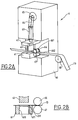
- the cutting station (6) shown in Figures 2A and 2B consists of a support (60) on which is mounted a matrix (61) comprising columns (63) on which a punch slides (62) actuated by a connecting rod (69), crank (64) assembly, eccentric (65) driven permanently by a motor.
- a passage (611) allows the installation of a photoelectric device (612) ensuring the detection of printed marks printed at proximity of each representative pattern on the card. The detection of the mark ensures the placement of patterns in opposite the punch to allow cutting on the fly and triggers the stop of the tape drive (13) which is provided by two rollers (66, 67) before the lowering the punch (62).
- At least one of these two rollers (66, 67) has a knurling on its edge (661, 662) which creates a corresponding knurling on the edge of the strip.
- the size of this knurling and the dimension of the strip (13) are provided so that the knurled parts are not in the surface which will subsequently constitute the card and which will be cut out in the cutting station (6), shown in Figure 1.
- a roller (68) disposed upstream of the two rollers drive (66, 67) is either associated with an arm pantographic and an electrical detection system to contact, either associated with a photoelectric system, to detect the size of the loop (133) formed on the ribbon (13) between the outlet of the drying device and entry into the device cutting (6) of the manufacturing process.
- printing speed will be accelerated or slowed down.
- the printing speed will increase and when the loop (133) arrives below a certain value, the speed of the printing stations (3, 4) is reduced. This allows you to adapt the printing speed to the cutting speed of the tool (6) which can reach a rate of 10 to 11,000 cards per hour while the printing device can reach a speed of 20m / s, which would require a tool with cadences significantly superior.
- Cards cut out of the press (6) are collected in batches and transferred to a chain of mounting of modular assemblies, as shown in Figure 3.
- This module assembly line has a rate of around 3,000 cards per hour. It is therefore desirable to have several channels in parallel.
- Each of the chains will include a device housing milling (7) in which a set of milling of the type described in the request for patent 93 04072 filed in the name of Gilles LEROUX S.A. est used. This operation is followed by an operation of pre-encoding (8) of the chip. Then the chip is placed on a modular support, cut and then inserted, as shown in step 9.
- the card with its module of integrated circuit is then brought to a set encoding and control (10) then is transported to a mat to pass in front of a counting camera (11) and then be collected in trays at station (12).
Landscapes
- Engineering & Computer Science (AREA)
- Manufacturing & Machinery (AREA)
- Microelectronics & Electronic Packaging (AREA)
- Credit Cards Or The Like (AREA)
- Shaping Of Tube Ends By Bending Or Straightening (AREA)
- Printing Methods (AREA)
Claims (14)
- Verfahren zur Herstellung von Karten mit Kunststoffträger, dadurch gekennzeichnet, daß es folgende Schritte enthält:Abwickeln und Geradebiegen eines Endlosbandes aus Kunststoff, dessen Abmessung geringfügig größer als eine der Abmessungen der Karte ist;Aufdrucken, in mindestens einer Druckstation (4a bis 4d), einer Folge von Druckmotiven und gedruckten Markierungen, von denen jede dem Motiv einer Karte in mindestens einer Druckfarbe entspricht;Antreiben des Bandes (13) mit einer geregelten Geschwindigkeit, die der Druck- und der Stanzgeschwindigkeit einer nach der Druckstation angeordneten Stanzstation (6) entspricht;Erfassen des Unterschieds zwischen der Druckgeschwindigkeit und der Stanzgeschwindigkeit;Ausstanzen des Bandes mit einer Presse (6) an Stellen, die durch die gedruckten Markierungen festgelegt sind, und in einem Takt, der nahe dem maximalen Takt der Presse ist;Regeln der Druckgeschwindigkeit in Abhängigkeit vom erfaßten Geschwindigkeitsunterschied zwischen der Druckgeschwindigkeit und der Stanzgeschwindigkeit.
- Verfahren nach Anspruch 1, dadurch gekennzeichnet, daß das Verfahren nach dem Druckvorgang und vor dem Stanzvorgang einen Trockenvorgang (51) enthält.
- Verfahren nach Anspruch 2, dadurch gekennzeichnet, daß der Trockenvorgang durch zwei Ultraviolett-Röhren (51r, 51v) erhalten wird, die bei einem doppelseitigen Druck auf der einen und der anderen Seite des Bandes (13) angeordnet sind.
- Verfahren zur Herstellung eines Kunststoffträgers nach einem der Ansprüche 1 bis 3, dadurch gekennzeichnet, daß es einen Schritt des Auftragens einer Lackschicht (4e) enthält, um den Druck vor dem Schritt des Ultraviolett-Trocknens (51) zu schützen.
- Verfahren zur Herstellung eines Kunststoffträgers nach einem der Ansprüche 1 bis 3, dadurch gekennzeichnet, daß es einen Schritt zum Auftragen einer Schutzschicht (131, 132) auf jede der bedruckten Flächen enthält.
- Vorrichtung zum Ausführen des Verfahrens nach einem der vorangehenden Ansprüche, mit einer Trägerspule (1) für ein Band (13) aus Kunststoff, um das Band anzudrehen und einer Vorrichtung (2) zum Geradebiegen zu liefern, wobei die Vorrichtung zum Geradebiegen das Band (13) mindestens einer Druckstation (4, 3) liefert, nach welcher eine Trockenstation (51) angeordnet ist, der Mittel (52, 53) zum Antreiben des Bandes und Mittel zum Erfassen des Geschwindigkeitsunterschieds zwischen der Druckgeschwindigkeit und der Stanzgeschwindigkeit einer nachfolgend angeordneten Stanzstation (6) zugeordnet sind.
- Vorrichtung nach Anspruch 6, dadurch gekennzeichnet, daß jede Druckstation mindestens eine Druckvorrichtung enthält, die aus einer Farbwalze besteht, die eine mit einer Gummiwalze (46) in Kontakt stehende Plattenträger-Walze (45) antreibt, wobei die Farbwalze (41) mit einer Walze (43) zum Andrücken der Farbschicht auf die Farbwalze in Abhängigkeit von der Relativgeschwindigkeit der Farbwalze und der Farbandruck-Walze zusammenwirkt, wobei die Breite jeder Walze (41 bis 46) in etwa einer der Abmessungen der Karte entspricht, wobei die Gummiwalze (46) mit einer Seite des Bandes (13) in Kontakt steht.
- Vorrichtung nach Anspruch 6, dadurch gekennzeichnet, daß jede Druckstation auf jeder Seite des Bandes (13) eine Druckvorrichtung enthält, die aus einer Farbwalze (41, 31) besteht, die eine mit einer Gummiwalze (46, 36) in Kontakt stehende Plattenträger-Walze (45, 35) antreibt, wobei die Farbwalze (41, 31) mit einer Walze (43, 33) zum Andrücken der Farbschicht auf die Farbwalze (41, 31) in Abhängigkeit von der Relativgeschwindigkeit der Farbwalze und der Farbandruck-Walze zusammenwirkt, wobei die Breite jeder Walze in etwa einer der Abmessungen der Karte entspricht, wobei die beiden Gummiwalzen (46, 36) auf der einen und der anderen Seite des Bandes mit diesem in Kontakt stehen.
- Vorrichtung nach einem der Ansprüche 6 bis 8, dadurch gekennzeichnet, daß die Presse eine Einheit aus Matrize (61) und Stempel (62) enthält, daß der auf Säulen angebrachte Stempel (62) von einer Einrichtung aus einem Schwingarm (69), einer Kurbel (64) und einem Exzenter (65) verschieblich angetrieben ist, wobei das Band von einer Einheit aus einer Antriebswalze (67) und einer Andrückwalze (66) angetrieben ist, so daß eine gedruckte Markierung gegenüber einer in der Matrize (61) angeordneten photoelektrischen Zelle (612) gebracht wird.
- Vorrichtung nach Anspruch 9, dadurch gekennzeichnet, daß das Antreiben des Bandes (13) von zwei Walzen (66, 67) gewährleistet ist, von welchen mindestens eine (66) an ihren beiden Enden über eine Länge gerändelt ist, der dem Bereich entspricht, der den Rand des Bandes (13) vom Rand des die Karte begrenzenden Ausschnitts trennt.
- Vorrichtung nach Anspruch 10, dadurch gekennzeichnet, daß die Druckstation mit einer Geschwindigkeit von unter 20 m/Sekunde arbeitet.
- Vorrichtung nach Anspruch 10, dadurch gekennzeichnet, daß die Stanzpresse in einem Takt zwischen 7000 und 13000 Karten pro Stunde arbeitet.
- Verwendung des Verfahrens zur Herstellung der Trägerkarten nach Anspruch 1 für die Herstellung einer Karte mit Mikroschaltungen, in welchem die ausgestanzten Karten in einer oder mehreren Fertigungsstraßen zum Einsetzen von Modulen übernommen werden, die in einem Takt arbeitet bzw. arbeiten, der niedriger ist als der Takt zur Herstellung der Kunststoffträger, um folgende Schritte auszuführen:Fräsen der Aufnahme (7);Vorcodieren (8) der Halbleiter-Mikroschaltungen;Stanzen und Einsetzen der aus einer Halbleiterschaltung gebildeten Modulen (9) in die Karten, wobei die Halbleiterschaltung auf einem Träger angebracht ist, der Kontaktflächen bildet;Codieren (10) und Kontrollieren der Karten.
- Verwendung des Herstellungsverfahrens nach Anspruch 13, dadurch gekennzeichnet, daß das Verfahren einen Schritt (11) des Zählens mittels einer Kamera und einen Schritt (12) des Einsetzens in Behälter enthält.
Priority Applications (3)
| Application Number | Priority Date | Filing Date | Title |
|---|---|---|---|
| FR9309810A FR2709038B1 (fr) | 1993-08-10 | 1993-08-10 | Procédé de fabrication pour support plastique, dispositif de fabrication pour un tel support et utilisation du procédé pour la fabrication de cartes à circuits intégrés. |
| DE69416134T DE69416134D1 (de) | 1994-10-28 | 1994-10-28 | Verfahren zur Herstellung von Kunststoffkartenträgern, Anordnung zur Durchführung des Verfahrens und Anwendung des Verfahrens für die Produktion von Mikroschaltungskarten |
| EP94402443A EP0710060B1 (de) | 1993-08-10 | 1994-10-28 | Verfahren zur Herstellung von Kunststoffkartenträgern, Anordnung zur Durchführung des Verfahrens und Anwendung des Verfahrens für die Produktion von Mikroschaltungskarten |
Applications Claiming Priority (2)
| Application Number | Priority Date | Filing Date | Title |
|---|---|---|---|
| FR9309810A FR2709038B1 (fr) | 1993-08-10 | 1993-08-10 | Procédé de fabrication pour support plastique, dispositif de fabrication pour un tel support et utilisation du procédé pour la fabrication de cartes à circuits intégrés. |
| EP94402443A EP0710060B1 (de) | 1993-08-10 | 1994-10-28 | Verfahren zur Herstellung von Kunststoffkartenträgern, Anordnung zur Durchführung des Verfahrens und Anwendung des Verfahrens für die Produktion von Mikroschaltungskarten |
Publications (2)
| Publication Number | Publication Date |
|---|---|
| EP0710060A1 EP0710060A1 (de) | 1996-05-01 |
| EP0710060B1 true EP0710060B1 (de) | 1999-01-20 |
Family
ID=26137548
Family Applications (1)
| Application Number | Title | Priority Date | Filing Date |
|---|---|---|---|
| EP94402443A Expired - Lifetime EP0710060B1 (de) | 1993-08-10 | 1994-10-28 | Verfahren zur Herstellung von Kunststoffkartenträgern, Anordnung zur Durchführung des Verfahrens und Anwendung des Verfahrens für die Produktion von Mikroschaltungskarten |
Country Status (2)
| Country | Link |
|---|---|
| EP (1) | EP0710060B1 (de) |
| FR (1) | FR2709038B1 (de) |
Families Citing this family (5)
| Publication number | Priority date | Publication date | Assignee | Title |
|---|---|---|---|---|
| US6551449B2 (en) | 1997-11-26 | 2003-04-22 | Hitachi, Ltd. | Thin electronic circuit component and method and apparatus for producing the same |
| JPH11161760A (ja) * | 1997-11-26 | 1999-06-18 | Hitachi Ltd | 薄型電子回路部品及びその製造方法及びその製造装置 |
| FR2785701B1 (fr) * | 1998-11-05 | 2001-08-31 | Leroux Gilles Sa | Procede de comptage de vignettes sur un film et dispositif specialement concu pour la mise en oeuvre de ce procede |
| US20040003734A1 (en) * | 2002-07-02 | 2004-01-08 | Shively J. Thomas | Method and apparatus for printing using an electrically conductive ink |
| KR100634327B1 (ko) * | 2005-04-13 | 2006-10-13 | 한국기계연구원 | 롤-투-롤 윤전인쇄방식을 이용한 전자소자의 제조방법 및그 제조장치 |
Family Cites Families (3)
| Publication number | Priority date | Publication date | Assignee | Title |
|---|---|---|---|---|
| US3652332A (en) * | 1970-07-06 | 1972-03-28 | American Can Co | Manufacture of printed circuits |
| DE2221727C3 (de) * | 1972-05-04 | 1978-08-24 | Dynamit Nobel Ag, 5210 Troisdorf | Vorrichtung zum Kalibrieren eines Wickelrohres aus thermoplastischem Kunststoff |
| GB2177262B (en) * | 1985-06-28 | 1988-08-10 | Gen Electric Co Plc | Electrical circuits |
-
1993
- 1993-08-10 FR FR9309810A patent/FR2709038B1/fr not_active Expired - Fee Related
-
1994
- 1994-10-28 EP EP94402443A patent/EP0710060B1/de not_active Expired - Lifetime
Also Published As
| Publication number | Publication date |
|---|---|
| FR2709038B1 (fr) | 1995-11-10 |
| EP0710060A1 (de) | 1996-05-01 |
| FR2709038A1 (fr) | 1995-02-17 |
Similar Documents
| Publication | Publication Date | Title |
|---|---|---|
| US5200253A (en) | Hologram forming sheet and process for producing the same | |
| EP0522217B2 (de) | Treuhanddokument oder Sicherheitsdokument mit Antifälschungsvorrichtung und Verfahren zur Herstellung eines solchen Dokumentes | |
| EP2886267A1 (de) | Verfahren und Vorrichtung zum Einbau eines Einsatzes in einen Hohlraum in einem Dünnschichtprodukt | |
| EP0985548A1 (de) | Sicherheitsdruckmaschine für Wertpapiere | |
| WO1999055530A1 (en) | Refractive overlaminate panel technique for the production of identification cards | |
| US20040101340A1 (en) | Ink-receptive card substrate | |
| WO1995031756A1 (fr) | Procede pour le transfert irreversible d'un reseau de diffraction, film de transfert et dispositif pour la mise en ×uvre du procede | |
| EP0710060B1 (de) | Verfahren zur Herstellung von Kunststoffkartenträgern, Anordnung zur Durchführung des Verfahrens und Anwendung des Verfahrens für die Produktion von Mikroschaltungskarten | |
| EP3094780B1 (de) | Erzeugung eines durchsichtigen fensters in einem sicherheitssubstrat für sicherheitsdruckanwendungen | |
| WO2001017796A1 (fr) | Installation d'impression par transfert, notamment par dorure | |
| CA2135731A1 (fr) | Procede de fabrication pour support plastique, dispositif de fabrication pour un tel support et utilisation du procede pour la fabrication de cartes a circuits integres | |
| US7150405B2 (en) | Method and device for producing a portable data carrier | |
| EP1192590B1 (de) | Verfahren zur herstellung einer kontaktlosen karte | |
| EP2681048A1 (de) | Vorrichtung zum übertragen einer schutzschicht für ein substrat bei hoher temperatur und unter druck sowie zugehöriges verfahren | |
| EP1147018B1 (de) | Verfahren und vorrichtung zur herstellung von personalisierten coupons | |
| EP3847035A1 (de) | Verfahren zur herstellung eines chipträgers mit oberflächeneffekt | |
| DE3685630T2 (de) | Vorrichtung zum foerdern einer leiterplattenbasis. | |
| FR2732642A1 (fr) | Procede de formation d'un ruban d'image graphique | |
| US5772834A (en) | Plastic substrate production production device | |
| EP2168082B1 (de) | Verfahren zur herstellung von mindestens eine elektronische einheit enthaltenden leiterplatten | |
| KR102949595B1 (ko) | 보호필름 제거장치 및 이를 구비하는 자동차 번호판 제조장치 | |
| US20040178625A1 (en) | Card-format data medium, method for the manufacture of such a data medium and lamination device for the manufacture of a card-format data medium | |
| KR102133032B1 (ko) | 기판에 오목부를 형성하는 방법 | |
| EP0624465B1 (de) | Vorrichtung zum zeitweiligen Verschweissen von Dokumenten auf einer Kunststoffbahn | |
| EP1268216B1 (de) | Rollenförmige druckplatte und verfahren zur herstellung |
Legal Events
| Date | Code | Title | Description |
|---|---|---|---|
| PUAI | Public reference made under article 153(3) epc to a published international application that has entered the european phase |
Free format text: ORIGINAL CODE: 0009012 |
|
| AK | Designated contracting states |
Kind code of ref document: A1 Designated state(s): BE CH DE ES FR GB IT LI LU NL |
|
| 17P | Request for examination filed |
Effective date: 19961025 |
|
| GRAG | Despatch of communication of intention to grant |
Free format text: ORIGINAL CODE: EPIDOS AGRA |
|
| 17Q | First examination report despatched |
Effective date: 19980227 |
|
| RAP1 | Party data changed (applicant data changed or rights of an application transferred) |
Owner name: C.K. INVESTISSEMENTS Owner name: GILLES LEROUX S.A. |
|
| GRAG | Despatch of communication of intention to grant |
Free format text: ORIGINAL CODE: EPIDOS AGRA |
|
| GRAH | Despatch of communication of intention to grant a patent |
Free format text: ORIGINAL CODE: EPIDOS IGRA |
|
| RAP1 | Party data changed (applicant data changed or rights of an application transferred) |
Owner name: ATN Owner name: GILLES LEROUX S.A. |
|
| GRAH | Despatch of communication of intention to grant a patent |
Free format text: ORIGINAL CODE: EPIDOS IGRA |
|
| GRAA | (expected) grant |
Free format text: ORIGINAL CODE: 0009210 |
|
| AK | Designated contracting states |
Kind code of ref document: B1 Designated state(s): BE CH DE ES FR GB IT LI LU NL |
|
| PG25 | Lapsed in a contracting state [announced via postgrant information from national office to epo] |
Ref country code: NL Free format text: LAPSE BECAUSE OF FAILURE TO SUBMIT A TRANSLATION OF THE DESCRIPTION OR TO PAY THE FEE WITHIN THE PRESCRIBED TIME-LIMIT Effective date: 19990120 Ref country code: IT Free format text: LAPSE BECAUSE OF FAILURE TO SUBMIT A TRANSLATION OF THE DESCRIPTION OR TO PAY THE FEE WITHIN THE PRE;WARNING: LAPSES OF ITALIAN PATENTS WITH EFFECTIVE DATE BEFORE 2007 MAY HAVE OCCURRED AT ANY TIME BEFORE 2007. THE CORRECT EFFECTIVE DATE MAY BE DIFFERENT FROM THE ONE RECORDED.SCRIBED TIME-LIMIT Effective date: 19990120 Ref country code: GB Free format text: LAPSE BECAUSE OF NON-PAYMENT OF DUE FEES Effective date: 19990120 Ref country code: ES Free format text: THE PATENT HAS BEEN ANNULLED BY A DECISION OF A NATIONAL AUTHORITY Effective date: 19990120 |
|
| REG | Reference to a national code |
Ref country code: CH Ref legal event code: EP |
|
| REF | Corresponds to: |
Ref document number: 69416134 Country of ref document: DE Date of ref document: 19990304 |
|
| PG25 | Lapsed in a contracting state [announced via postgrant information from national office to epo] |
Ref country code: DE Free format text: LAPSE BECAUSE OF FAILURE TO SUBMIT A TRANSLATION OF THE DESCRIPTION OR TO PAY THE FEE WITHIN THE PRESCRIBED TIME-LIMIT Effective date: 19990421 |
|
| NLV1 | Nl: lapsed or annulled due to failure to fulfill the requirements of art. 29p and 29m of the patents act | ||
| GBV | Gb: ep patent (uk) treated as always having been void in accordance with gb section 77(7)/1977 [no translation filed] |
Effective date: 19990120 |
|
| PG25 | Lapsed in a contracting state [announced via postgrant information from national office to epo] |
Ref country code: LU Free format text: LAPSE BECAUSE OF NON-PAYMENT OF DUE FEES Effective date: 19991028 |
|
| PG25 | Lapsed in a contracting state [announced via postgrant information from national office to epo] |
Ref country code: LI Free format text: LAPSE BECAUSE OF NON-PAYMENT OF DUE FEES Effective date: 19991031 Ref country code: CH Free format text: LAPSE BECAUSE OF NON-PAYMENT OF DUE FEES Effective date: 19991031 Ref country code: BE Free format text: LAPSE BECAUSE OF NON-PAYMENT OF DUE FEES Effective date: 19991031 |
|
| PLBE | No opposition filed within time limit |
Free format text: ORIGINAL CODE: 0009261 |
|
| STAA | Information on the status of an ep patent application or granted ep patent |
Free format text: STATUS: NO OPPOSITION FILED WITHIN TIME LIMIT |
|
| 26N | No opposition filed | ||
| BERE | Be: lapsed |
Owner name: S.A. GILLES LEROUX Effective date: 19991031 |
|
| REG | Reference to a national code |
Ref country code: CH Ref legal event code: PL |
|
| PG25 | Lapsed in a contracting state [announced via postgrant information from national office to epo] |
Ref country code: FR Free format text: LAPSE BECAUSE OF NON-PAYMENT OF DUE FEES Effective date: 20000630 |
|
| REG | Reference to a national code |
Ref country code: FR Ref legal event code: ST |