EP0711038B1 - IGBT-Treiberschaltung und Zündvorrichtung - Google Patents
IGBT-Treiberschaltung und Zündvorrichtung Download PDFInfo
- Publication number
- EP0711038B1 EP0711038B1 EP95116812A EP95116812A EP0711038B1 EP 0711038 B1 EP0711038 B1 EP 0711038B1 EP 95116812 A EP95116812 A EP 95116812A EP 95116812 A EP95116812 A EP 95116812A EP 0711038 B1 EP0711038 B1 EP 0711038B1
- Authority
- EP
- European Patent Office
- Prior art keywords
- voltage
- resistor
- switching element
- igbt
- gate
- Prior art date
- Legal status (The legal status is an assumption and is not a legal conclusion. Google has not performed a legal analysis and makes no representation as to the accuracy of the status listed.)
- Expired - Lifetime
Links
- 230000010355 oscillation Effects 0.000 claims description 23
- 238000001514 detection method Methods 0.000 claims description 15
- 238000007599 discharging Methods 0.000 claims description 11
- 239000004065 semiconductor Substances 0.000 claims description 11
- 238000004804 winding Methods 0.000 claims description 7
- 238000010586 diagram Methods 0.000 description 5
- 238000002485 combustion reaction Methods 0.000 description 4
- 230000020169 heat generation Effects 0.000 description 4
- 238000005259 measurement Methods 0.000 description 2
- 230000003321 amplification Effects 0.000 description 1
- 230000001934 delay Effects 0.000 description 1
- 230000005669 field effect Effects 0.000 description 1
- 238000003199 nucleic acid amplification method Methods 0.000 description 1
- 230000001629 suppression Effects 0.000 description 1
Images


Classifications
-
- H—ELECTRICITY
- H03—ELECTRONIC CIRCUITRY
- H03K—PULSE TECHNIQUE
- H03K17/00—Electronic switching or gating, i.e. not by contact-making and –breaking
- H03K17/51—Electronic switching or gating, i.e. not by contact-making and –breaking characterised by the components used
- H03K17/56—Electronic switching or gating, i.e. not by contact-making and –breaking characterised by the components used by the use, as active elements, of semiconductor devices
- H03K17/567—Circuits characterised by the use of more than one type of semiconductor device, e.g. BIMOS, composite devices such as IGBT
-
- H—ELECTRICITY
- H03—ELECTRONIC CIRCUITRY
- H03K—PULSE TECHNIQUE
- H03K17/00—Electronic switching or gating, i.e. not by contact-making and –breaking
- H03K17/04—Modifications for accelerating switching
- H03K17/0406—Modifications for accelerating switching in composite switches
-
- H—ELECTRICITY
- H03—ELECTRONIC CIRCUITRY
- H03K—PULSE TECHNIQUE
- H03K17/00—Electronic switching or gating, i.e. not by contact-making and –breaking
- H03K17/16—Modifications for eliminating interference voltages or currents
- H03K17/161—Modifications for eliminating interference voltages or currents in field-effect transistor switches
- H03K17/165—Modifications for eliminating interference voltages or currents in field-effect transistor switches by feedback from the output circuit to the control circuit
-
- H—ELECTRICITY
- H03—ELECTRONIC CIRCUITRY
- H03K—PULSE TECHNIQUE
- H03K17/00—Electronic switching or gating, i.e. not by contact-making and –breaking
- H03K17/16—Modifications for eliminating interference voltages or currents
- H03K17/168—Modifications for eliminating interference voltages or currents in composite switches
Definitions
- the present invention relates generally to a driving circuit for IGBT (insulated-gate type bipolar transistor) and, more particularly, to a constant current circuit which controls a primary current of an ignition coil of an internal combustion engine ignition device used in various automotive vehicles.
- IGBT insulated-gate type bipolar transistor
- NPN transistors 25 and 26 are connected in Darlington configuration.
- the collector current Ic of the Darlington transistor is detected by a primary current detecting resistor 27 to control the collector current Ic of the Darlington transistor.
- a comparator 28 compares the detection voltage across the primary current detecting resistor 27 with a comparison voltage and controls a base current control transistor (NPN transistor) 29 thereby to control the base current I B of the Darlington transistor.
- NPN transistor base current control transistor
- an oscillation suppressing resistor 30 is connected between the base terminal of the Darlington transistor and the detection terminal side of the comparator 28.
- the base current I B is suppressed from oscillation even when the current value detected by the primary current detecting resistor 27 is less than a predetermined value.
- the greater base current I B is required therefor.
- the electric power consumed by a base current control transistor (driving transistor) 31 which turns on and off in response to an ignition signal IGt and by a base current limiting resistor (driving resistor) 32 becomes greater and electric circuit components of greater power capacity are required. That is, the driving transistor 31 and the driving resistor 32 must amplify the current by the determined current amplifying factor h FE thereby to increase the collector current Ic of the bipolar transistors while the driving resistor 32 must have a resistance value of about several hundreds of ohms thereby to increase the collector current Ic of the bipolar transistors flowing through the driving resistor 32. Thus, both the driving resistor 32 and the driving transistor 31 require greater electric power capacity.
- IGBT insulated-gate type bipolar transistor
- a driving circuit according to the preamble of claim 1 is known from document US-A-5 045 964.
- a driving switching element driven by a driving signal applies a predetermined voltage to a gate terminal of an IGBT.
- a comparator compares a voltage corresponding to a voltage produced across terminals of a current detecting resistor with a comparison voltage and turns on and off a constant current control transistor based on the comparison result thereof so that a gate voltage of the IGBT is adjusted to keep the current flowing through the IGBT at a constant value.
- An oscillation suppressing resistor feeds back the gate voltage of the IGBT to the detection terminal side of the comparator to suppress the oscillation of the current flowing to the IGBT.
- a charge/discharge control resistor connected between the gate terminal of the IGBT and the oscillation suppressing resistor slows down a speed of charging and discharging of a stray capacitance of the IGBT thereby to stabilize the current flowing through the IGBT.
- a semiconductor element connected in parallel with the charge/discharge control resistor is provided to speed up the discharging speed only, avoid heat generation of the IGBT caused by a switching delay and avoid secondary voltage drop of the ignition coil.
- the IGBT is connected in series with a primary winding of an ignition coil of an ignition device for an internal combustion engine.
- the IGBT 2 has, as illustrated in the figure, an FET (field effect transistor) connected across the base-emitter path of a bipolar transistor and has a gate terminal (electrode), collector terminal and an emitter terminal.
- an electric current (a primary current I1 of the ignition coil 1) flows from the battery terminal 19 to the ground through the primary winding 1a of the ignition coil 1, IGBT 2 and the current detecting resistor 3.
- the current detecting resistor 3 converts the magnitude of the current I1 to a voltage value.
- a junction "a” between the emitter terminal of the IGBT 2 and the current detecting resistor 3 is connected to the non-inverting input terminal (detection terminal) of a comparator 10 through a series circuit of resistors 7, 8 and 9.
- a junction "b" between the resistors 7 and 8 is grounded through a resistor 11.
- a junction "c” between the resistors 5 and 6 and a junction “d” between the resistors 8 and 9 are connected to each other through an oscillation suppressing resistor 12.
- the oscillation suppressing resistor 12 divides the voltage across the gate-emitter path of the IGBT 2 to provide the comparator 10 with a positive feedback.
- the gate-emitter voltage is divided by the oscillation suppressing resistor 12 and a combined resistor network in which the resistor 8 is connected in series with the resistor 11 connected in parallel to the serially-connected resistors 3 and 7.
- the junction “h” between the driving PNP transistor 4 and the resistor 5 is grounded through a series circuit of resistors 13 and 14 and a junction “e” between the resistors 13 and 14 is connected to an inverting input terminal of the comparator 10 to provide the comparison voltage.
- the comparator 10 is supplied with the voltage of the junction "d" and the ground voltage.
- the comparator 10 compares a voltage corresponding to the voltage produced across the current detecting resistor 3 at the junction "a", i.e., a voltage corresponding to the primary current I1 of the ignition coil 1, with a divided voltage (comparison voltage) divided by the resistors 13 and 14.
- the comparator 10 produces an L-level or H-level signal based on the comparison of the two input voltages.
- a junction "f” same as the junction "c" between the resistors 5 and 6 is grounded through an NPN transistor 15 used as a constant current control switching element.
- the base terminal of the NPN transistor 15 is connected to the output terminal of the comparator 10.
- the NPN transistor 15 turns on and off in response to the H-level and L-level output signals of the comparator 10, respectively.
- the driving transistor 4 When the ignition signal (driving signal) IGt is applied to the driving PNP transistor 4, the driving transistor 4 turns on. Then, the constant voltage Vcc is applied to the charge/discharge control resistor 6 through the resistor 5 and the IGBT 2 turns on. With the turning on of the IGBT 2, the electric current (primary current I1 of the ignition coil 1) starts to flow from the battery terminal (V B ) 19 to the ground side through the primary winding 1a, IGBT 2 and the current detecting resistor 3 at the timing t1 in Fig. 2A.
- the primary current I1 is converted to the voltage by the current detecting resistor 3 and the comparator 10 compares this detection voltage with the comparison voltage.
- the comparator 10 applies the L-level signal to the base terminal of the NPN transistor 15. With the L-level signal applied to the base terminal, the NPN transistor 15 is kept turned off to increase the primary current I1.
- the comparator 10 applies the H-level signal to the base terminal of the NPN transistor 15 to turn on the NPN transistor 15 which in turn lowers the gate voltage of the IGBT 2.
- the NPN transistor 15 turns on and off in response to the output signal of the comparator 10 and, by adjusting the gate voltage of the IGBT 2, keeps the current flowing to the IGBT 2 constant.
- the gate voltage of the IGBT 2 is fed back through the oscillation suppressing resistor 12 to the detection terminal side of the comparator 10 thereby to suppress the oscillation of the current flowing to the IGBT 2.
- the speed of charging and discharging of the gate input capacitance Ciss pulled down by the NPN transistor 15 is slowed down by the charge/discharge control resistor 6. Therefore, the value of the primary current I1 of the ignition coil 1 is stabilized and does not change instantaneously. That is, without the charge/discharge control resistor 6, the gate voltage of the IGBT 2 is pulled down instantaneously to the L-level by the NPN transistor 15 to cause the oscillation of the primary current I1 of the ignition coil 1.
- the response speed of the positive feedback is slowed down (CR time constant is increased) and the charging and discharging speed of the gate input capacitance Ciss is slowed down or smoothed to suppress oscillation.
- the collector current Ic of 7A can be produced.
- the required electric power capacity of the driving transistor 4 may be less than that required in the case of the conventional circuit configuration illustrated in Fig. 8.
- the gate input capacitance Ciss of the IGBT 2 is from 1,000pF to 2,000pF in this embodiment.
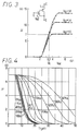
- the result of measurement of the discharging speed is illustrated in Fig. 4. It will be understood from this measurement result that the appropriate resistance value of the charge/discharge control resistor 6 is from 500 to 10K ⁇ and the heat generation of the IGBT 2 (proportional to Ic and V CE ) due to switching delay is expected to be reduced.
- diode 16 may be connected parallelly to the charge/discharge control resistor 6 in opposite direction to the charging direction to slow down the discharging speed only.
- the embodiment illustrated in Fig. 5 is modified in that a series circuit of a resistor 17 and a driving NPN transistor 18 is connected between the constant voltage source Vcc (5V) and the ground and the gate terminal of the IGBT 2 is connected to a junction "h" between the resistor 17 and the driving NPN transistor 18.
- the required electric power capacity of the driving transistors and the driving resistors may be less than that in Fig. 8.
- the embodiment of Fig. 1, however, is more practical than the embodiment of Fig. 5, because it requires no driving resistor 17 used in the embodiment of Fig. 5 and the voltage applied to the gate terminal of the IGBT 2 does not fall due to the current flowing into a control circuit portion.
- the charge/discharge control resistor 6 is provided between the gate terminal of the IGBT 2 and the oscillation suppressing resistor 12. As a result, the gate voltage of the IGBT 2 is fed back to the detection terminal side of the comparator 10 through the oscillation suppressing resistor 12 and the charge/discharge control resistor 6 and the oscillation is suppressed.
- the charge/discharge control resistor 6 slows down the speed of charging and discharging of the stray capacitance of the IGBT 2 thereby to stabilize the constant current value (primary current value of the ignition coil).
- the diode 16 which is connected as illustrated in Fig. 5 in parallel with the charge/discharge control resistor 6 to allow the current flow only in the direction of discharging, speeds up only the discharging speed so that heat generation of the IGBT caused by the switching delay may be avoided.
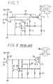
- the voltage dividing circuit configuration in the embodiments of Figs. 1 and 5 may be modified as illustrated in Figs. 6 and 7, respectively. More specifically, the resistor 8 in Fig. 1 may be eliminated as illustrated in Fig. 6 and the resistor 8 in Fig. 5 may be eliminated as illustrated in Fig. 7.
- diode 16 is connected to the ends of the charge/discharge control resistor 6 in Fig. 7, it may be connected to the ends of a series connection of the resistors 5 and 6 as in the embodiment of Fig. 5.
- An IGBT driving circuit includes an IGBT (2) connected in series with a primary winding (1a) of an ignition coil (1) and a current detecting resistor (3).
- a transistor (4) is connected to the gate of the IGBT to apply a gate voltage in response to an ignition signal.
- a comparator (10) compares a voltage produced across the current detecting resistor (3) with a comparison voltage.
- An NPN transistor (15) connected to the gate of the IGBT turns on and off in response to the comparison result of the comparator to adjust the gate voltage. The gate voltage is fed back to the detection terminal side of the comparator for oscillation suppression through an oscillation suppressing resistor (12).
- a charge/discharge control resistor (6) is connected between the gate of the IGBT and the oscillation suppressing resistor and a diode (16) is connected in parallel with . the charge/discharge control resistor, so that the electric current (I1) flowing through the IGBT is maintained constant.
Landscapes
- Ignition Installations For Internal Combustion Engines (AREA)
Claims (4)
- Treiberschaltung für ein Halbleiter-Schaltelement, das eine Streukapazität aufweist und mit einer elektrischen Last verbunden ist, mit:einem Gatespannungs-Eingangsanschluß (d), der mit einem Gateanschluß (g) des Halbleiter-Schaltelements (2) verbunden ist, zum Anlegen einer vorherbestimmten Spannung als Gatespannung;einem Stromerfassungs-widerstand (3), der in Reihe mit dem Halbleiter-Schaltelement geschaltet ist;einem Vergleicher (10) zum Vergleichen einer Erfassungsspannung mit einer Vergleichsspannung, wobei die Erfassungsspannung einer Erfassungsanschlußseite des Vergleichers zugeführt wird und einer längs dem Stromerfassungs-widerstand erzeugten Spannung entspricht;einem Konstantstrom-Steuerschaltelement (15), das mit dem Gateanschluß des Halbleiter-Schaltelements verbunden ist, zum Ein- und Ausschalten in Reaktion auf Vergleichsergebnisse des Vergleichers, um die Gatespannung des Gateanschlusses des Halbleiterschaltelements einzustellen, so daß ein durch das Halbleiterschaltelement fließender elektrischer Strom konstant gehalten wird;ein Lade-/Entladesteuerwiderstand (6), der zwischen dem Gateanschluß des Halbleiterschaltelements und dem Konstantstrom-Steuerschaltelement geschaltet ist; gekennzeichnet durcheinen Schwingungsunterdrückungs-Widerstand (12), der zwischen dem Lade-/Entladesteuerwiderstand und der Erfassungsanschlußseite des Vergleichers geschaltet ist, zum Rückkoppeln der Gatespannung zu der Erfassungsanschlußseite des Vergleichers, damit ein Schwingen des elektrischen Stroms unterdrückt wird.
- Treiberschaltung nach Anspruch 1, wobei das Halbleiterschaltelement ein IGBT ist.
- Treiberschaltung nach Anspruch 1 oder 2, mit einem zweiten Halbleiterschaltelement (16), das parallel zu dem Lade-/Entladesteuerwiderstand geschaltet ist, für einen elektrischen Stromfluß ausschließlich in einer Entladerichtung.
- Treiberschaltung nach einem der Ansprüche 1 bis 3, wobei die elektrische Last eine Zündspule (1) mit einer Primärwicklung (1a) aufweist, die in Reihe mit dem erstgenannten Halbleiterschaltelement geschaltet ist.
Applications Claiming Priority (3)
| Application Number | Priority Date | Filing Date | Title |
|---|---|---|---|
| JP27149094A JP3477852B2 (ja) | 1994-11-04 | 1994-11-04 | Igbt駆動回路および点火装置 |
| JP271490/94 | 1994-11-04 | ||
| JP27149094 | 1994-11-04 |
Publications (3)
| Publication Number | Publication Date |
|---|---|
| EP0711038A2 EP0711038A2 (de) | 1996-05-08 |
| EP0711038A3 EP0711038A3 (de) | 1998-02-11 |
| EP0711038B1 true EP0711038B1 (de) | 2000-03-08 |
Family
ID=17500783
Family Applications (1)
| Application Number | Title | Priority Date | Filing Date |
|---|---|---|---|
| EP95116812A Expired - Lifetime EP0711038B1 (de) | 1994-11-04 | 1995-10-25 | IGBT-Treiberschaltung und Zündvorrichtung |
Country Status (5)
| Country | Link |
|---|---|
| US (1) | US5603308A (de) |
| EP (1) | EP0711038B1 (de) |
| JP (1) | JP3477852B2 (de) |
| DE (1) | DE69515417T2 (de) |
| ES (1) | ES2144559T3 (de) |
Cited By (1)
| Publication number | Priority date | Publication date | Assignee | Title |
|---|---|---|---|---|
| US9006988B2 (en) | 2010-10-22 | 2015-04-14 | Delta Electronics, Inc. | Method of controlling ignition circuit and ignition circuit using the same |
Families Citing this family (28)
| Publication number | Priority date | Publication date | Assignee | Title |
|---|---|---|---|---|
| US6100728A (en) * | 1995-07-31 | 2000-08-08 | Delco Electronics Corp. | Coil current limiting feature for an ignition coil driver module |
| JP2734420B2 (ja) * | 1995-08-30 | 1998-03-30 | 日本電気株式会社 | 定電圧源回路 |
| EP0780570B1 (de) * | 1995-12-18 | 2002-08-14 | Fuji Electric Co., Ltd. | Halbleiterzündschaltungsvorrichtung mit Strombegrenzung für eine Brennkraftmaschine |
| JPH1051285A (ja) * | 1996-05-28 | 1998-02-20 | Mitsubishi Electric Corp | 電圧制御型トランジスタの駆動回路 |
| DE19648144A1 (de) * | 1996-11-21 | 1998-05-28 | Bosch Gmbh Robert | Wechselstrom-Zündsystem für einen Motor |
| WO1998049444A1 (en) * | 1997-04-25 | 1998-11-05 | Hitachi, Ltd. | Ignition system |
| JP3530714B2 (ja) * | 1997-05-26 | 2004-05-24 | 株式会社日立製作所 | 内燃機関用点火装置 |
| DE19741963C1 (de) * | 1997-09-23 | 1999-03-11 | Siemens Ag | Vorrichtung zur Unterdrückung unerwünschter Zündungen bei einem Ottomotor |
| JP3713521B2 (ja) * | 1997-11-10 | 2005-11-09 | 東北電力株式会社 | 電源装置およびこれが搭載される電気自動車 |
| JP3482161B2 (ja) * | 1999-08-03 | 2003-12-22 | 株式会社日立製作所 | 内燃機関の点火システム |
| DE602004009524T2 (de) * | 2004-01-22 | 2008-07-31 | Stmicroelectronics S.R.L., Agrate Brianza | Dynamische Steuerung eines Leistungstransistors bei Hochspannungsanwendungen |
| JP4411535B2 (ja) | 2004-05-11 | 2010-02-10 | 株式会社デンソー | 内燃機関用点火装置 |
| US7080639B1 (en) | 2005-06-30 | 2006-07-25 | Visteon Global Technologies, Inc. | Soft IGBT turn-on ignition applications |
| DE102007063721B4 (de) * | 2006-03-22 | 2014-05-08 | Denso Corporation | Schaltkreis mit einem Transistor und einer Ansteuerschaltung zur Ansteuerung des Transistors |
| JP2008002392A (ja) * | 2006-06-23 | 2008-01-10 | Denso Corp | 車載電子機器の出力回路 |
| JP5201321B2 (ja) * | 2007-12-04 | 2013-06-05 | 富士電機株式会社 | イグナイタシステム |
| JP2010045141A (ja) * | 2008-08-11 | 2010-02-25 | Fuji Electric Systems Co Ltd | 半導体装置および内燃機関用点火装置 |
| US9181920B2 (en) * | 2011-04-04 | 2015-11-10 | Federal-Mogul Ignition Company | System and method for detecting arc formation in a corona discharge ignition system |
| CN104054232B (zh) * | 2012-01-30 | 2016-11-02 | Nec能源元器件株式会社 | 用于控制蓄电池组的电力存储系统、方法以及蓄电池组 |
| JP6354430B2 (ja) * | 2014-08-01 | 2018-07-11 | 富士電機株式会社 | 半導体装置 |
| JP6395565B2 (ja) * | 2014-11-11 | 2018-09-26 | ローム株式会社 | イグナイタおよび車両 |
| JP6690246B2 (ja) * | 2016-01-12 | 2020-04-28 | 富士電機株式会社 | 半導体装置 |
| JP6707874B2 (ja) * | 2016-01-29 | 2020-06-10 | 富士電機株式会社 | 半導体装置 |
| CN106533423B (zh) * | 2016-09-21 | 2024-04-19 | 宇通客车股份有限公司 | 一种脉冲接口电路 |
| JP7143398B2 (ja) * | 2018-03-13 | 2022-09-28 | ローム株式会社 | スイッチ制御回路、イグナイタ |
| JP6772355B1 (ja) * | 2019-10-15 | 2020-10-21 | 株式会社京三製作所 | スイッチングモジュール |
| CN111487514B (zh) * | 2020-04-20 | 2022-07-22 | 全球能源互联网研究院有限公司 | 一种igbt动态参数测试电路杂散电容提取方法及系统 |
| CN114441926B (zh) * | 2022-02-16 | 2022-12-09 | 广州科肯电气有限公司 | Igbt退饱和检测电路 |
Family Cites Families (6)
| Publication number | Priority date | Publication date | Assignee | Title |
|---|---|---|---|---|
| JPS6143825A (ja) * | 1984-08-08 | 1986-03-03 | Toshiba Corp | ゲ−トドライブ回路 |
| US5045964A (en) * | 1990-04-30 | 1991-09-03 | Motorola, Inc. | Thermal clamp for an ignition coil driver |
| JPH04143457A (ja) * | 1990-10-04 | 1992-05-18 | Mitsubishi Electric Corp | 内燃機関点火装置の電流制限回路 |
| US5397964A (en) * | 1992-06-01 | 1995-03-14 | Motorola, Inc. | Reflected energy adaptive inductive load driver and method therefor |
| JP2837054B2 (ja) * | 1992-09-04 | 1998-12-14 | 三菱電機株式会社 | 絶縁ゲート型半導体装置 |
| EP0615342A3 (de) * | 1993-03-10 | 1995-03-22 | Fuji Electric Co Ltd | Halbleitervorrichtung. |
-
1994
- 1994-11-04 JP JP27149094A patent/JP3477852B2/ja not_active Expired - Fee Related
-
1995
- 1995-10-25 ES ES95116812T patent/ES2144559T3/es not_active Expired - Lifetime
- 1995-10-25 DE DE69515417T patent/DE69515417T2/de not_active Expired - Lifetime
- 1995-10-25 EP EP95116812A patent/EP0711038B1/de not_active Expired - Lifetime
- 1995-11-01 US US08/551,342 patent/US5603308A/en not_active Expired - Lifetime
Cited By (1)
| Publication number | Priority date | Publication date | Assignee | Title |
|---|---|---|---|---|
| US9006988B2 (en) | 2010-10-22 | 2015-04-14 | Delta Electronics, Inc. | Method of controlling ignition circuit and ignition circuit using the same |
Also Published As
| Publication number | Publication date |
|---|---|
| EP0711038A2 (de) | 1996-05-08 |
| JPH08135547A (ja) | 1996-05-28 |
| US5603308A (en) | 1997-02-18 |
| ES2144559T3 (es) | 2000-06-16 |
| DE69515417D1 (de) | 2000-04-13 |
| JP3477852B2 (ja) | 2003-12-10 |
| DE69515417T2 (de) | 2000-09-07 |
| EP0711038A3 (de) | 1998-02-11 |
Similar Documents
| Publication | Publication Date | Title |
|---|---|---|
| EP0711038B1 (de) | IGBT-Treiberschaltung und Zündvorrichtung | |
| US5967128A (en) | Ignition apparatus for an internal combustion engine | |
| JPH02223672A (ja) | 半導体電力装置における過度の熱散逸に対して電流制御及び防護を与えるユニットのための診断回路 | |
| EP0881739A1 (de) | Fahrzeuggenerator-Steuervorrichtung | |
| EP0622717B1 (de) | Temperaturstabilisierte Entladestromrückleitungsschaltung zum Treiben einer induktiven Last | |
| JP3030076B2 (ja) | 電流制御回路 | |
| GB1570972A (en) | Ignition system including threshold circuit | |
| US4602205A (en) | Battery voltage regulating system | |
| CA1160279A (en) | Control of rising and falling times of the drive signal of a brushless dc motor | |
| US5453678A (en) | Programmable-output voltage regulator | |
| US5107190A (en) | Means and method for optimizing the switching performance of power amplifiers | |
| US4556838A (en) | Electronic switch | |
| US5585748A (en) | Voltage-frequency converter circuit with temperature compensation | |
| US4492213A (en) | Ignition system for internal combustion engines | |
| US4420971A (en) | Device for flowthrough rate measurement in an internal combustion engine | |
| EP0040688B1 (de) | Kontaktloses Zündsystem für Brennkraftmaschinen mit Speisespannungskompensation | |
| US4899715A (en) | Ignition device for internal combustion engine | |
| US20020027391A1 (en) | Reduced current and power consumption structure of drive circuit | |
| US4570199A (en) | Protection circuit for voltage regulator of vehicle mounted generator | |
| US4567388A (en) | Clamp circuit | |
| US6424187B1 (en) | Driving apparatus for power MOS transistor | |
| US4617906A (en) | Dwell control for an I.C. engine spark ignition system | |
| US4225796A (en) | Frequency-to-current conversion circuit | |
| JPS5934868B2 (ja) | 無接点点火装置 | |
| JPS63239368A (ja) | 内燃機関点火装置 |
Legal Events
| Date | Code | Title | Description |
|---|---|---|---|
| PUAI | Public reference made under article 153(3) epc to a published international application that has entered the european phase |
Free format text: ORIGINAL CODE: 0009012 |
|
| AK | Designated contracting states |
Kind code of ref document: A2 Designated state(s): DE ES FR GB IT |
|
| RAP1 | Party data changed (applicant data changed or rights of an application transferred) |
Owner name: DENSO CORPORATION |
|
| PUAL | Search report despatched |
Free format text: ORIGINAL CODE: 0009013 |
|
| AK | Designated contracting states |
Kind code of ref document: A3 Designated state(s): DE ES FR GB IT |
|
| 17P | Request for examination filed |
Effective date: 19980630 |
|
| GRAG | Despatch of communication of intention to grant |
Free format text: ORIGINAL CODE: EPIDOS AGRA |
|
| 17Q | First examination report despatched |
Effective date: 19990601 |
|
| GRAG | Despatch of communication of intention to grant |
Free format text: ORIGINAL CODE: EPIDOS AGRA |
|
| GRAH | Despatch of communication of intention to grant a patent |
Free format text: ORIGINAL CODE: EPIDOS IGRA |
|
| GRAH | Despatch of communication of intention to grant a patent |
Free format text: ORIGINAL CODE: EPIDOS IGRA |
|
| GRAA | (expected) grant |
Free format text: ORIGINAL CODE: 0009210 |
|
| AK | Designated contracting states |
Kind code of ref document: B1 Designated state(s): DE ES FR GB IT |
|
| ITF | It: translation for a ep patent filed | ||
| REF | Corresponds to: |
Ref document number: 69515417 Country of ref document: DE Date of ref document: 20000413 |
|
| ET | Fr: translation filed | ||
| REG | Reference to a national code |
Ref country code: ES Ref legal event code: FG2A Ref document number: 2144559 Country of ref document: ES Kind code of ref document: T3 |
|
| PLBE | No opposition filed within time limit |
Free format text: ORIGINAL CODE: 0009261 |
|
| STAA | Information on the status of an ep patent application or granted ep patent |
Free format text: STATUS: NO OPPOSITION FILED WITHIN TIME LIMIT |
|
| 26N | No opposition filed | ||
| REG | Reference to a national code |
Ref country code: GB Ref legal event code: IF02 |
|
| PGFP | Annual fee paid to national office [announced via postgrant information from national office to epo] |
Ref country code: FR Payment date: 20131022 Year of fee payment: 19 Ref country code: DE Payment date: 20131021 Year of fee payment: 19 Ref country code: GB Payment date: 20131021 Year of fee payment: 19 |
|
| PGFP | Annual fee paid to national office [announced via postgrant information from national office to epo] |
Ref country code: IT Payment date: 20131028 Year of fee payment: 19 Ref country code: ES Payment date: 20131029 Year of fee payment: 19 |
|
| REG | Reference to a national code |
Ref country code: DE Ref legal event code: R119 Ref document number: 69515417 Country of ref document: DE |
|
| GBPC | Gb: european patent ceased through non-payment of renewal fee |
Effective date: 20141025 |
|
| PG25 | Lapsed in a contracting state [announced via postgrant information from national office to epo] |
Ref country code: DE Free format text: LAPSE BECAUSE OF NON-PAYMENT OF DUE FEES Effective date: 20150501 Ref country code: GB Free format text: LAPSE BECAUSE OF NON-PAYMENT OF DUE FEES Effective date: 20141025 |
|
| REG | Reference to a national code |
Ref country code: FR Ref legal event code: ST Effective date: 20150630 |
|
| PG25 | Lapsed in a contracting state [announced via postgrant information from national office to epo] |
Ref country code: FR Free format text: LAPSE BECAUSE OF NON-PAYMENT OF DUE FEES Effective date: 20141031 Ref country code: IT Free format text: LAPSE BECAUSE OF NON-PAYMENT OF DUE FEES Effective date: 20141025 |
|
| REG | Reference to a national code |
Ref country code: ES Ref legal event code: FD2A Effective date: 20151126 |
|
| PG25 | Lapsed in a contracting state [announced via postgrant information from national office to epo] |
Ref country code: ES Free format text: LAPSE BECAUSE OF NON-PAYMENT OF DUE FEES Effective date: 20141026 |