EP0712201A2 - Système de protection contre les surintensités de courant pour convertisseurs de puissance électroniques à GTO - Google Patents
Système de protection contre les surintensités de courant pour convertisseurs de puissance électroniques à GTO Download PDFInfo
- Publication number
- EP0712201A2 EP0712201A2 EP95202958A EP95202958A EP0712201A2 EP 0712201 A2 EP0712201 A2 EP 0712201A2 EP 95202958 A EP95202958 A EP 95202958A EP 95202958 A EP95202958 A EP 95202958A EP 0712201 A2 EP0712201 A2 EP 0712201A2
- Authority
- EP
- European Patent Office
- Prior art keywords
- current
- gto
- protection system
- gtos
- converter
- Prior art date
- Legal status (The legal status is an assumption and is not a legal conclusion. Google has not performed a legal analysis and makes no representation as to the accuracy of the status listed.)
- Withdrawn
Links
- 238000010304 firing Methods 0.000 claims abstract description 32
- 238000010791 quenching Methods 0.000 claims abstract description 25
- 230000000171 quenching effect Effects 0.000 claims abstract description 23
- 238000001514 detection method Methods 0.000 claims 3
- 230000002401 inhibitory effect Effects 0.000 claims 1
- 230000004913 activation Effects 0.000 description 12
- 230000000295 complement effect Effects 0.000 description 9
- 230000005764 inhibitory process Effects 0.000 description 7
- 230000001681 protective effect Effects 0.000 description 4
- 230000000875 corresponding effect Effects 0.000 description 3
- 238000010586 diagram Methods 0.000 description 3
- 239000004065 semiconductor Substances 0.000 description 3
- 230000033228 biological regulation Effects 0.000 description 2
- 230000015556 catabolic process Effects 0.000 description 2
- 230000001934 delay Effects 0.000 description 2
- 230000000694 effects Effects 0.000 description 2
- 238000009413 insulation Methods 0.000 description 2
- 108010028778 Complement C4 Proteins 0.000 description 1
- 230000005355 Hall effect Effects 0.000 description 1
- 101100449816 Saccharomyces cerevisiae (strain ATCC 204508 / S288c) GTO1 gene Proteins 0.000 description 1
- 239000004020 conductor Substances 0.000 description 1
- 230000002596 correlated effect Effects 0.000 description 1
- 230000007423 decrease Effects 0.000 description 1
- 230000003111 delayed effect Effects 0.000 description 1
- 230000001066 destructive effect Effects 0.000 description 1
- 238000010438 heat treatment Methods 0.000 description 1
- 230000001939 inductive effect Effects 0.000 description 1
- 238000000034 method Methods 0.000 description 1
- 230000000737 periodic effect Effects 0.000 description 1
- 230000001105 regulatory effect Effects 0.000 description 1
- 230000000630 rising effect Effects 0.000 description 1
- 238000004513 sizing Methods 0.000 description 1
- 230000001360 synchronised effect Effects 0.000 description 1
Images

Classifications
-
- H—ELECTRICITY
- H02—GENERATION; CONVERSION OR DISTRIBUTION OF ELECTRIC POWER
- H02M—APPARATUS FOR CONVERSION BETWEEN AC AND AC, BETWEEN AC AND DC, OR BETWEEN DC AND DC, AND FOR USE WITH MAINS OR SIMILAR POWER SUPPLY SYSTEMS; CONVERSION OF DC OR AC INPUT POWER INTO SURGE OUTPUT POWER; CONTROL OR REGULATION THEREOF
- H02M7/00—Conversion of AC power input into DC power output; Conversion of DC power input into AC power output
- H02M7/42—Conversion of DC power input into AC power output without possibility of reversal
- H02M7/44—Conversion of DC power input into AC power output without possibility of reversal by static converters
- H02M7/48—Conversion of DC power input into AC power output without possibility of reversal by static converters using discharge tubes with control electrode or semiconductor devices with control electrode
- H02M7/505—Conversion of DC power input into AC power output without possibility of reversal by static converters using discharge tubes with control electrode or semiconductor devices with control electrode using devices of a thyratron or thyristor type requiring extinguishing means
- H02M7/515—Conversion of DC power input into AC power output without possibility of reversal by static converters using discharge tubes with control electrode or semiconductor devices with control electrode using devices of a thyratron or thyristor type requiring extinguishing means using semiconductor devices only
- H02M7/521—Conversion of DC power input into AC power output without possibility of reversal by static converters using discharge tubes with control electrode or semiconductor devices with control electrode using devices of a thyratron or thyristor type requiring extinguishing means using semiconductor devices only in a bridge configuration
Definitions
- the present invention relates to a current overload protection system for GTO electronic power converters, in particular for converters for the supply of three phase asynchronous traction motors and the like.
- GTOs are electronic power components which are becoming ever more widespread in use in converters for converting DC into AC because, as opposed to usual controlled diodes or thyristors they can be controlled to fire and be quenched via a control electrode or "gate".
- GTOs have a maximum current value above which gate-controlled quenching cannot take place even though they are able to conduct for a long time a current greater than the maximum which can be quenched.
- a GTO receives a quenching command whilst the current which flows through it is greater than the maximum value, it is subject to permanent damage.
- a GTO supports voltages between anode and cathode up to a maximum predetermined value and in order to avoid the inductive component of the impedance of the load or of the voltage source from causing, at quenching, voltage overloads greater than the maximum admissible voltage, it is necessary to use, in parallel with the GTO's overvoltage limitation circuits, so-called “snubbers", essentially RC networks which charge upon quenching, remain charged for the whole of the time that the GTO is quenched, and discharge exponentially through the GTO when this is fired.
- the minimum firing time is equal to three times the time constant of the snubber to allow the snubber to become 95% discharged.
- the most critical malfunctioning situation is a short circuit, in which the current is not limited by the load and can rapidly reach values very much higher than the maximum current which can be quenched by the GTO.
- the short circuit may be outside the converter, typically be accidental contact between two outputs or by breakdown of the load insulation, or internal due to failure or malfunctioning of a power component (for example the failed quenching of a complementary GTO).
- a second solution consists in the use of an auxiliary power semiconductor intended to impede or limit the flow of excess currents in the GTO.
- the excess current can be diverted onto a thyristor disposed in parallel to but is not limited by the GTO, and must be switched off in some way.
- an inductor positioned in series with the supply to the converter to be protected, limits the rising rate of the current and, when the current reaches a threshold greater than the normal maximum working current of the GTO of the converter, but less than the maximum current which can be quenched by the GTO, allows a timed procedure for immediate inhibition of firing of a quenched GTO and immediate or deferred quenching of a fired GTO to take place as a function of the respective instant of firing and in any event in a sufficiently short time to prevent the current from reaching non quenchable levels even in the case of a short circuit.
- the maximum quenching delay is less than the minimum firing time of GTOs set to allow the complete discharge of the associated snubbers with them but is in any event sufficient to ensure at least 50% discharge thereof.
- the maximum quenching delay is equal to the time constant of the snubbers in such a way that these are 66% discharged. This ensures that the voltage overload at quenching is contained within non-destructive limits of the GTO whilst quenching in these conditions is not repeated with excessive frequency.
- a power diode which is normally reversed biased is connected in parallel with the inductor in such a way as to allow the current which flows in the inductor to continue to flow in the inductor and in the diode when the GTOs are quenched.
- This current falls according to the time constant defined by the resistance of the inductor and by its inductance.
- the protection system is reset automatically when the current in the inductor falls below the threshold value at which intervention is caused, that is with a variable delay in dependence on the quenching delay and the consequent magnitude of the excess current.
- the automatic resetting is limited to a predetermined time interval after which it is no longer possible.
- FIG. 1 With reference to Figure 1 there is shown a three phase converter formed by six GTOs 1, 2, 3, 4, 5, 6 connected in a known way in pairs in series 1 and 4, 2 and 5, 3 and 6 and a DC voltage source +V completed by a conventional ground.
- the converter is connected to the voltage source via an inductor 9 in parallel with a diode 10 the cathode of which is connected to the voltage source +V.
- each pair of GTOs is connected to a three phase load 7, in the application illustrated a synchronous motor, which is thus supplied with a suitable sequence of voltage pulses.
- the gate electrodes of the GTOs 1, 2, 3, which when fired each connect one phase of the load to the voltage +V are identified with the letters R, S, T, whilst the gate electrodes of the GTOs 4, 5, 6 which are respectively complementary to the GTOs 1, 2, 3 are identified with the letters R , S , T , respectively.
- the supply to the load is obtained by simultaneously firing at least one of the GTOs 1, 2, 3 (or high side GTO) and at least one of the low side GTOs which is not complementary to the fired high side GTO.
- the simultaneous firing of GTOs 1 and 5 causes application of the voltage +V between the two phases R and S of the load and firing of GTOs 4 and 2 complementary to the previous ones, causes application of the voltage +V across the two phases S and R of the load, that is to say the application of the voltage -V across the phases R and S.
- the firing of the different GTOs is controlled by a regulation system 8 which, in a known manner, and in dependence on a variable to be regulated, for example the speed "s" of the motor, generates a plurality of duration modulation signals PW (R, R , S, S T, T ,) which when asserted control firing of the corresponding GTOs.
- a regulation system 8 which, in a known manner, and in dependence on a variable to be regulated, for example the speed "s" of the motor, generates a plurality of duration modulation signals PW (R, R , S, S T, T ,) which when asserted control firing of the corresponding GTOs.
- timing logic units respectively 11, 12, 13, 14, 15, 16 which generate control signals respectively PWR1, PWS1, PWT1, PW R 1, PW S 1, PW T 1.
- each unit which controls firing and quenching of a predetermined GTO receives, as a firing inhibition signal, the signal PWX1 emitted by the unit which controls firing of the complementary GTO .
- the unit 11 which generates the signal PWR1 receives the signal PW R 1 from the unit 14 and sends the signal PWR1 to the unit 14.
- Each unit receives, from a common protection unit 17, a general GTO firing consent signal NINH and a signal ENB which allows the GTO to be maintained in its fired state for a predetermined minimum time interval.
- the common protection unit 17 is controlled by a maximum current signal IMAX generated by a comparator 18 which receives a reference signal VREF at its inverting input and at its non-inverting input receives a voltage signal I(S) proportional to the current input to the converter.
- the current input to the converter is preferably detected by a Hall effect sensor 19 in order to avoid resistive dissipations.
- the senor 19 is disposed in the loop formed by conductor 9 and diode 10 so as to detect not only the current delivered to the converter but also possible currents which circulate in the loop.
- each GTO cannot be fired simultaneously with its complementary GTO, even though two GTOs one high side and one low side can be simultaneously fired, in normal operating conditions there is always only one high side GTO and one low side GTO in a fired state and the current input by the inverter is the whole of the current which flows in one of the fired GTOs.
- the overload condition of the converter is therefore also an excess current condition for at least one of the GTOs.
- the excess current condition is essentially due to the joint firing of one GTO and its complementary GTO and to the consequent short circuit of the converter, and the contribution to the current input to the converter due to the other GTOs which may be fired is secondary.
- the inductor 9 ensures that independently of the load impedance, and therefore also in the case of a short circuit, the rate of variation of current with time is less than a predetermined value in such a way that within the intervention time envisaged for the protection, the current does not rise from the excess current level which causes protective intervention to a value greater than the maximum quenching current of the GTOs.
- the inductance of the inductor must be as far below the load impedance as possible and preferably is chosen in such a way that in a time interval equal to the time constant of the snubber the variations in current resulting from a short circuit lie between 20% and 30% of the maximum current quenchable by the GTOs.
- the signals ENB and NINH are deasserted and the logic units from 11 to 16 are controlled, as long as NINH is deasserted, to prevent any firing of the GTOs and, as long as ENB is deasserted, to control the quenching of any fired GTOs after a predetermined time has elapsed from their firing, less than the minimum firing time required for discharge of the associated snubber.
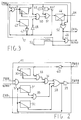
- the logic unit 11 of Figure 2 which is essentially a timing logic unit, comprises three univibrators 30, 31, 32 or equivalent timing devices, four two-input AND logic gates 33, 34, 35, 37, one logic OR gate 38, a driving interface circuit or driver 39 and a logic NOT element 40.
- the logic unit 11 for protection of the GTO1 ( Figure 1) on the high side of the R phase receives four signals at its input:
- the signal PW R 1 is applied to the input of the NOT 40 the output of which is connected to the activation input of the univibrator 30 and to one input of the AND gate 33 the second input of which is connected to the negative output Q of the univibrator 30.
- the output of the AND gate 33 is connected to one input of the AND gate 34 the second input of which is connected to the output of the AND gate 37.
- the output of the AND gate 34 is connected to one input of the OR gate 38 the output of which is connected to the input of the driver 39 and to the activation input of the univibrators 31, 32.
- the direct output of the univibrator 32 is connected to one input of the OR 38.
- the direct output of the univibrator 31 is connected to one input of the AND gate 35 which receives the signal ENB at its second input and the output of which is connected to one input of the OR gate 38.
- the operation of the unit 11 is very simple.
- the received signal PWR is transferred to the output as a signal PWR1 with only the propagation delays of the logic chain.
- the signal PWR1 controls firing of GTO 1 and, having being sent to the logic output 14 ( Figure 1) prevents this from asserting signal PW R 1.
- the output of the AND gate 33 thus rises to the logic level 1 only after a time interval defined by the activation time of the univibrator 30 and enables the AND gate 34 with a predetermined delay.
- the inhibition intervention is on the other hand immediate and as soon as PW R 1 is asserted the gate 34 is disabled.
- the activation time of the univibrator 31 is for example of the order of 72 ⁇ sec and corresponds to time necessary for the snubber associated with the GTO 1 to discharge almost completely.
- the activation time of the univibrator 32 is shorter and, for example, of the order of 24 ⁇ sec, equal to the time constant of the snubber, and corresponds to the time necessary for the snubber associated with the GTO 1 to discharge partially by about 63%.
- the AND gate 35 is disabled and the signal PWR1 already asserted is deasserted with immediate or delayed effect in dependence on the state of the univibrator 32, in particular on the delay in the deasserted signal ENB relative to the assertion instant of PWR.
- Figure 3 shows the block circuit diagram of a protection unit 17 common to all the GTOs, the function of which is to generate the signals NINH and ENB.
- the unit 17 comprises two univibrators 41, 42, a counter 43, an RS flip flop 44 and logic gates such as two two-input AND gates 45, 46, NOT elements 47, 48, one three-input AND gate 50, one OR gate 51 and one NOR gate 52.
- the unit 17 receives at its input the signal IMAX which, when asserted is indicative of overload or short circuit, and a manual reset signal RM.
- the signal IMAX is applied to one input of the AND gate 43, to one input of the NOR gate 52, to one input of the counter 43 which increments at each assertion of IMAX, and to one input of the AND gate 50.
- the output of the AND gate 45 is connected to the activation inputs of the univibrators 41, 42.
- the inverted output Q of the univibrator 41 is connected to a second input of the AND gate 50.
- the direct output of the univibrator 42 is connected to the input of the NOT 47 the output of which is connected to the second output of the AND gate 45, to the reset input of the counter 43 and to the input of a NOT 49 the output of which is connected to a third input of the AND gate 50 the output of which is connected to one input of the OR 51.
- the OR 51 receives an output signal from the counter 43 asserted when the counter reaches a predetermined count value.
- the output of the OR gate 51 is connected to the set input of the flip flop 44 which receives the manual reset signal RM at its reset input.
- the output of the NOR 52 is connected to one input of the AND gate 46 which receives the signal GEN at a second input.
- the signal NINH is made available at the output of the AND gate 46.
- the operation of the unit 17 is also very simple.
- the signal ENB is asserted, as is the signal NINH, if enabled by the external control unit 53 (GEN asserted).
- the signal IMAX is asserted and the signals ENB and NINH are immediately deasserted and remain deasserted for the whole of the time that IMAX is asserted, that is to say for the whole of the time that the current which flows in the switch is greater than the predetermined value.
- the univibrators 41, 42 have an activation period of suitable duration and define an automatic reset time interval (univibrator 41) in which new firing and quenching operations of the converter are possible and a subsequent automatic reset inhibition time interval during which a possible overload causes locking of the converter and of the protection system with the necessity of external intervention for resetting.
- the activation period T1 of the univibrator 42 is conveniently greater than that (T2) of the univibrator 41.
- T1 can be of the order of 200 msec and T2 of the order of 400 msec.
- the operation of the univibrator 41 (the negative output of which is connected to one input of the AND gate 50) is to prevent, for the whole of the time interval T1, the signal IMAX, applied to the input of the AND gate 50, from being able to put the flip flop 44 into its set state.
- the univibrator 42 performs a triple function: on the one hand, for the whole of the period T2 in which it is activated, it prevents the univibrators 41 and 42 from being reactivated by possible subsequent assertions of IMAX; on the other hand (via the NOT 47, 48) it prevents the intrinsic activation delays of the univibrator 41 relative to the assertion of IMAX being able to cause improper setting of the flip flop 44.
- IMAX activates the univibrators 41 and 42 and causes, upon deassertion of ENB and NINH, inhibition of firing of the GTOs and quenching of those which are fired, in this case with a convenient delay.
- the flip flop 44 is put into its set state.
- the various univibrators can be replaced by counters activated by a periodic timing signal generated by an oscillator and different logic elements from those indicated, such as analogue devices, can be used in different but functionally equivalent electrical circuit arrangements. It is also possible to subject the automatic resetting of the protection system rather than to the fact that the current in the inductor 9 and in the recirculation diode 10 has fallen to a predetermined level, to the fact that the current absorbed by the inverter has fallen to a predetermined level, therefore indicating that the overload is over.
- the current sensor it is sufficient, as indicated in broken outline in Figure 1 with 19a, for the current sensor to be disposed in a branch of the supply line through which flows current effectively absorbed by the inverter rather than in the recirculation circuit formed by the inductor 9 and the diode 10.
- This time may be variable as a function of the preceding history of the protection system and, for example, may increase as a function of the number of protective interventions already performed.
Landscapes
- Engineering & Computer Science (AREA)
- Power Engineering (AREA)
- Inverter Devices (AREA)
- Power Conversion In General (AREA)
Applications Claiming Priority (2)
| Application Number | Priority Date | Filing Date | Title |
|---|---|---|---|
| IT94MI002266A IT1275653B1 (it) | 1994-11-09 | 1994-11-09 | Sistema di protezione di sovracorrente per convertitore elettronico di potenza a gto |
| ITMI942266 | 1994-11-09 |
Publications (2)
| Publication Number | Publication Date |
|---|---|
| EP0712201A2 true EP0712201A2 (fr) | 1996-05-15 |
| EP0712201A3 EP0712201A3 (fr) | 1997-09-24 |
Family
ID=11369820
Family Applications (1)
| Application Number | Title | Priority Date | Filing Date |
|---|---|---|---|
| EP95202958A Withdrawn EP0712201A3 (fr) | 1994-11-09 | 1995-11-02 | Système de protection contre les surintensités de courant pour convertisseurs de puissance électroniques à GTO |
Country Status (2)
| Country | Link |
|---|---|
| EP (1) | EP0712201A3 (fr) |
| IT (1) | IT1275653B1 (fr) |
Cited By (3)
| Publication number | Priority date | Publication date | Assignee | Title |
|---|---|---|---|---|
| WO2003026118A1 (fr) * | 2001-09-21 | 2003-03-27 | Abb Ab | Convertisseur resonant auxiliaire a commutation de polarite (arcp) et son procede de commande |
| DE102005009069B4 (de) * | 2004-09-02 | 2008-05-29 | Mitsubishi Denki K.K. | Steuerschaltung einer Leistungs-Halbleiter-Vorrichtung und steuernde integrierte Schaltung |
| EP3334023A1 (fr) * | 2016-12-07 | 2018-06-13 | General Electric Technology GmbH | Améliorations apportées ou se rapportant aux convertisseurs à commutation par ligne |
Family Cites Families (2)
| Publication number | Priority date | Publication date | Assignee | Title |
|---|---|---|---|---|
| JPS5963983A (ja) * | 1982-10-04 | 1984-04-11 | Hitachi Ltd | 電力変換器の制御装置 |
| DE3246706A1 (de) * | 1982-12-17 | 1984-06-20 | Danfoss As | Stromversorgungsvorrichtung fuer einen wechselstromverbraucher |
-
1994
- 1994-11-09 IT IT94MI002266A patent/IT1275653B1/it active IP Right Grant
-
1995
- 1995-11-02 EP EP95202958A patent/EP0712201A3/fr not_active Withdrawn
Non-Patent Citations (1)
| Title |
|---|
| None |
Cited By (4)
| Publication number | Priority date | Publication date | Assignee | Title |
|---|---|---|---|---|
| WO2003026118A1 (fr) * | 2001-09-21 | 2003-03-27 | Abb Ab | Convertisseur resonant auxiliaire a commutation de polarite (arcp) et son procede de commande |
| US6995994B2 (en) | 2001-09-21 | 2006-02-07 | Abb Ab | Converter and a method for controlling a converter |
| DE102005009069B4 (de) * | 2004-09-02 | 2008-05-29 | Mitsubishi Denki K.K. | Steuerschaltung einer Leistungs-Halbleiter-Vorrichtung und steuernde integrierte Schaltung |
| EP3334023A1 (fr) * | 2016-12-07 | 2018-06-13 | General Electric Technology GmbH | Améliorations apportées ou se rapportant aux convertisseurs à commutation par ligne |
Also Published As
| Publication number | Publication date |
|---|---|
| ITMI942266A0 (it) | 1994-11-09 |
| IT1275653B1 (it) | 1997-10-17 |
| ITMI942266A1 (it) | 1996-05-09 |
| EP0712201A3 (fr) | 1997-09-24 |
Similar Documents
| Publication | Publication Date | Title |
|---|---|---|
| US11139808B2 (en) | Semiconductor device and power conversion system | |
| EP0701313B1 (fr) | Disjoncteur et circuit de limitation de tension | |
| US5946178A (en) | Protective circuit for series-connected power semiconductors | |
| US20020030411A1 (en) | Excessive load capacitor detection circuit for UPS | |
| US4884182A (en) | Current source power converting apparatus with overvoltage protection | |
| US4432032A (en) | Auxiliary voltage snubber circuit | |
| JPH0410316B2 (fr) | ||
| US6104149A (en) | Circuit and method for improving short-circuit capability of IGBTs | |
| US9847642B2 (en) | Control circuit | |
| JPH114150A (ja) | 半導体装置とこの半導体装置を用いた電力変換装置 | |
| EP0470525B1 (fr) | Convertisseur de puissance avec protection contre le courant transversal | |
| US10756721B2 (en) | Short circuit protection for a gate driver using pulsed operation | |
| US5057987A (en) | Fault detection and protection strategy for a pair of complementary GTO thyristors | |
| EP0712201A2 (fr) | Système de protection contre les surintensités de courant pour convertisseurs de puissance électroniques à GTO | |
| US11271495B2 (en) | Intermediate circuit coupling in drive assemblies | |
| US5105324A (en) | Device for protecting semiconductor circuits against transients on the supply line | |
| US5990724A (en) | Method and a device for detecting and handling short-circuit phenomena for power semiconductor devices of turn-off type connected in series | |
| US4942494A (en) | Short-circuit protector for a half-controlled three-phase bridge | |
| US4853835A (en) | Protective apparatus for inverter | |
| US5235487A (en) | Inverter with overload current protection | |
| JP3661813B2 (ja) | 電圧駆動形半導体素子の駆動回路 | |
| US4636932A (en) | dv/dt Protection circuit device for an AC-DC converter apparatus | |
| EP3742568A1 (fr) | Circuit de protection de surtension, convertisseur de puissance, dispositif d'entraînement électrique et véhicule | |
| JP3722649B2 (ja) | 3レベルインバータ | |
| US4782419A (en) | Inhibitable static switch for an AC electric circuit including an inductive load |
Legal Events
| Date | Code | Title | Description |
|---|---|---|---|
| PUAI | Public reference made under article 153(3) epc to a published international application that has entered the european phase |
Free format text: ORIGINAL CODE: 0009012 |
|
| AK | Designated contracting states |
Kind code of ref document: A2 Designated state(s): BE DE ES FR GB SE |
|
| PUAL | Search report despatched |
Free format text: ORIGINAL CODE: 0009013 |
|
| AK | Designated contracting states |
Kind code of ref document: A3 Designated state(s): BE DE ES FR GB SE |
|
| STAA | Information on the status of an ep patent application or granted ep patent |
Free format text: STATUS: THE APPLICATION IS DEEMED TO BE WITHDRAWN |
|
| 18D | Application deemed to be withdrawn |
Effective date: 19981201 |