EP0713154A2 - Dispositif d'impression et méthode - Google Patents
Dispositif d'impression et méthode Download PDFInfo
- Publication number
- EP0713154A2 EP0713154A2 EP95117917A EP95117917A EP0713154A2 EP 0713154 A2 EP0713154 A2 EP 0713154A2 EP 95117917 A EP95117917 A EP 95117917A EP 95117917 A EP95117917 A EP 95117917A EP 0713154 A2 EP0713154 A2 EP 0713154A2
- Authority
- EP
- European Patent Office
- Prior art keywords
- recording surface
- write head
- recording
- roller
- dielectric
- Prior art date
- Legal status (The legal status is an assumption and is not a legal conclusion. Google has not performed a legal analysis and makes no representation as to the accuracy of the status listed.)
- Granted
Links
Images


Classifications
-
- G—PHYSICS
- G03—PHOTOGRAPHY; CINEMATOGRAPHY; ANALOGOUS TECHNIQUES USING WAVES OTHER THAN OPTICAL WAVES; ELECTROGRAPHY; HOLOGRAPHY
- G03G—ELECTROGRAPHY; ELECTROPHOTOGRAPHY; MAGNETOGRAPHY
- G03G15/00—Apparatus for electrographic processes using a charge pattern
- G03G15/22—Apparatus for electrographic processes using a charge pattern involving the combination of more than one step according to groups G03G13/02 - G03G13/20
- G03G15/32—Apparatus for electrographic processes using a charge pattern involving the combination of more than one step according to groups G03G13/02 - G03G13/20 in which the charge pattern is formed dotwise, e.g. by a thermal head
- G03G15/321—Apparatus for electrographic processes using a charge pattern involving the combination of more than one step according to groups G03G13/02 - G03G13/20 in which the charge pattern is formed dotwise, e.g. by a thermal head by charge transfer onto the recording material in accordance with the image
- G03G15/325—Apparatus for electrographic processes using a charge pattern involving the combination of more than one step according to groups G03G13/02 - G03G13/20 in which the charge pattern is formed dotwise, e.g. by a thermal head by charge transfer onto the recording material in accordance with the image using a stylus or a multi-styli array
-
- B—PERFORMING OPERATIONS; TRANSPORTING
- B41—PRINTING; LINING MACHINES; TYPEWRITERS; STAMPS
- B41J—TYPEWRITERS; SELECTIVE PRINTING MECHANISMS, i.e. MECHANISMS PRINTING OTHERWISE THAN FROM A FORME; CORRECTION OF TYPOGRAPHICAL ERRORS
- B41J2/00—Typewriters or selective printing mechanisms characterised by the printing or marking process for which they are designed
- B41J2/385—Typewriters or selective printing mechanisms characterised by the printing or marking process for which they are designed characterised by selective supply of electric current or selective application of magnetism to a printing or impression-transfer material
- B41J2/39—Typewriters or selective printing mechanisms characterised by the printing or marking process for which they are designed characterised by selective supply of electric current or selective application of magnetism to a printing or impression-transfer material using multi-stylus heads
-
- G—PHYSICS
- G03—PHOTOGRAPHY; CINEMATOGRAPHY; ANALOGOUS TECHNIQUES USING WAVES OTHER THAN OPTICAL WAVES; ELECTROGRAPHY; HOLOGRAPHY
- G03G—ELECTROGRAPHY; ELECTROPHOTOGRAPHY; MAGNETOGRAPHY
- G03G15/00—Apparatus for electrographic processes using a charge pattern
- G03G15/22—Apparatus for electrographic processes using a charge pattern involving the combination of more than one step according to groups G03G13/02 - G03G13/20
- G03G15/32—Apparatus for electrographic processes using a charge pattern involving the combination of more than one step according to groups G03G13/02 - G03G13/20 in which the charge pattern is formed dotwise, e.g. by a thermal head
- G03G15/321—Apparatus for electrographic processes using a charge pattern involving the combination of more than one step according to groups G03G13/02 - G03G13/20 in which the charge pattern is formed dotwise, e.g. by a thermal head by charge transfer onto the recording material in accordance with the image
Definitions
- the invention relates to an apparatus and method for printing, more particularly to an apparatus and method for electrophoretic and dielectrophoretic printing.
- Digital systems for producing print media have become widespread in the field of graphic printing.
- the systems typically work with a digital database, based on the printing forms, and either on a plate that is then mounted in a press or deposited on the press roll of a press.
- the print information can be recorded in the form of binary signals, which together represent the "signature image".
- These plates or rollers are always separated according to the main color components of the original image, e.g. cyan, magenta, yellow and black.
- the color components can be obtained sequentially or simultaneously with parallel recording heads.
- the recording heads used in prior art devices are characterized by: 1) a plurality of laser beams which travel across the plate or the cylinder line by line at high speed, 2) a plurality of laser diodes which spiral through the recording medium when writing several lines, or 3) groups (arrays) of light-emitting diodes (LEDs) for the serial recording of a spiral-shaped pattern, which represents a single-color sheet.
- the recording medium is sensitive to light, and this always requires a light-tight recording and pressure chamber in prior art devices to prevent accidental exposure of the recording medium.
- the first method uses a waterless method for picking up offset ink and then transferring it to the printing substrate.
- the second method uses a special, liquid electrostatic toner made of charged particles, and these particles are electrostatically deposited on the printing component and from there on an offset cloth, which in turn transfers the toner electrostatically to a sheet of paper or other printing medium.
- dry toner is xerographically deposited on the photosensitive printing component, from where the toner is transferred directly to the printing medium using a standard xerographic method.
- a writing station Arranged around the printing roller is a writing station with a printhead, an inking station via which different-colored thermoplastic printing inks can be dispensed, and an ink transfer station, which is actually the gap between the two rollers.
- a printhead responsive to incoming data is stored on the platen while successive revolutions of the same emit electronic latent images representing the color components or signatures of an original image, and each such image consists of a pattern of electrostatic charge areas or dots, the field strengths of which correspond to Gray or color values vary.
- thermoplastic printing inks the actual colors of which, as a rule, but not necessarily, match the colors of the surface mentioned images recorded on the printhead. These colors usually include cyan, magenta, yellow and black in subtractive color printing.
- the field lines from the electrostatic charge areas or pixels that make up the latent image cause "pieces" of the melted ink to be removed from the application head.
- the field lines can change briefly when passing under the application head or not, depending on the presence of grounded or pre-stressed components of the application head.
- the amounts of the color elements are directly proportional to the field strengths of the charge areas.
- the surface of the printing roller in spite of its color-phobic nature, receives variable amounts of color at these image points, which are related to the field strengths at these points, the latent image on this surface is effectively obtained.
- the color is held on this surface by electrostatic forces when the developed images are transported to the ink transfer station.
- the colors - still in the molten state on the printing roller - and the relatively cool paper on the paper roller are rotated through the gap between the two rollers.
- the ink changes phase so that the color changes from a liquid state to a solid state, so that the ink is immediately transferred to the paper.
- electrostatic images can be recorded on a platen or other printing component with a printhead similar to that described in the above patent.
- the pressure component has one anisotropic recording surface so that the electrostatic charge areas created on that surface by the printhead result in uniform or inhomogeneous electrostatic fields at the location of each picture element (pixel) with a field beyond the surface of the printing component. If these charged areas of the printing component are moved against the development medium, ie dielectric printing ink or toner, the field induces an electrical dipole moment in the medium in question by dielectric polarization. The polarized medium obtained is drawn through the field gradient to the area of maximum field strength.
- the polarization charge at one end of the medium in the stronger field is pulled more towards the stronger field, while the opposite and equal polarization charge at the other end of the medium is pushed back less strongly in the other direction because the field there is weaker.
- the development medium thus migrates to the areas of the pressure component in which the fields are strongest and adheres there. Dielectrophoretic printing therefore enables electrostatic printing without the need for charged ink or charged toner particles. This means that while the development medium is polarized because the positive and negative charges are located on the medium due to the presence of a uniform electrostatic field, the net charge on the medium is zero.
- a uniform electric field on the dielectric surface of a printing component, such as a printing roller can be obtained in various ways. For example, as the Dr. Kuehnle provides for writing on the surface with a wire on which there is a periodically varying voltage, for example alternating voltage or rectified alternating voltage (direct voltage), the amplitude of the voltage varying in accordance with the digital input signal on the printing device.
- the uniform field for the printing component can be brought about by the structure of the printing component itself.
- the printing component can be provided with a dielectric surface that is anisotropic in that it contains a pattern of conductive paths that extend from the surface of the dielectric layer to a ground plane below that layer.
- One way to obtain these grounded areas or field endpoints on the dielectric layer is to form the layer so that it contains many crystallites with so-called grain boundaries, the electrical conductivity of which is considerably greater than that within the crystallites themselves.
- 5,315,061 describes a donor or development roller for transferring a charged toner onto a photoconductor belt for developing a latent image on the photoconductor belt.
- the donor roller is made of metal and small dielectric bodies are distributed over the surface. When friction is charged on the entire surface of the donor roller, electrostatic fields are formed between the dielectric bodies and the metal surface. Small closed electric fields - so-called "microfields" - are thus formed on the surface of the donor roller. These microfields help attract the charged toner to the surface of the donor roller. A squeegee then sets the toner to a uniform thickness.
- the donor roller according to US Pat. No.
- 5,315,061 provides a homogeneous and uniform amount of charged toner so that an image can be developed on a photoconductor belt. No images are written directly on the donor roller, rather the images are written on the photoconductor tape.
- U.S. Patent No. 3,739,748 shows a donor roller for transferring charged toner onto a xerographic drum.
- the donor roller has a dielectric surface which is contacted by pins connected to a voltage source.
- the pens cannot write images on the donor roller, but rather only facilitate the gray value reproduction of the image which is written on the xerographic drum by an exposure device. Neither of these two donor rollers and no related devices cause inhomogeneous microfields over the surface of a printing component.
- the present invention accordingly aims at specifying a device with which strong fields of inhomogeneous nature can be maintained over the surface of the printing component.
- Another purpose of the invention is to provide such a device that is relatively easy to manufacture.
- Another purpose of the invention is to provide a device with a printing component on which very high resolution electronic images can be recorded.
- Yet another purpose of the invention is to provide effective types of write heads in conjunction with a dielectric surface that can record high resolution electronic images.
- Other purposes are likely to be apparent in part and will be apparent in part from the following. Accordingly, the invention included features of construction, combination of elements, and arrangement of parts, as will be exemplified from the following detailed description, and the scope of the invention is defined in the claims.
- the printing component includes a substrate that supports a thin layer of dielectric material, the resistivity of which is very high, for example about 1015 ohms / cm, to prevent premature discharge.
- a conductive layer can be provided in the middle between the substrate and the dielectric layer. This conductive layer can be grounded or can remain ungrounded, as will be described below in connection with the various embodiments.
- a pattern of minute conductive areas or dots may be present on the work surface or within the dielectric layer. If present, the dots are preferably periodic with a period at least equal to or smaller than the size of a resolution element or picture element (pixel) of the electronic image that is on the printing component to be recorded.
- the conductive points made of a material with a lower specific resistance than that of the dielectric are preferably metallic, but in certain applications can also be electrically connected to the conductive level below the dielectric layer.
- an adhesive coating covers the surfaces of the dielectric layer and the conductive dots, so that the recording surface of the printing component is slightly ink-phobic.
- the cross sections of the points can be circular, but various other shapes are also possible, including rectangular or toroidal.
- electrical charges can be applied to the recording surface of the print component by a microtunnel type print or write head, as described in U.S. Patent No. 5,325,120. Typically, these charges represent an image recorded on the print component. These charges result in uniform electric fields that are strongest around the conductive dots.
- the mean voltage around each point is also a monotonous function of the gray value at the relevant point in the electronic image.
- An important aspect is that the uniform fields generated by the conductive dots on the dielectric surface of the recording component extend beyond the surface.
- the electric fields induce an electric dipole moment in the medium by dielectric polarization, and the medium becomes proportional to the strengths of the charged surfaces of the recording surface by dielectrophoresis Charges pulled.
- the development medium thus accumulates around each conductive point in an amount that is monotonous with the field strength at the point in question increases, thereby developing the electronic image recorded on the printing component.
- Non-uniform fields can be obtained on a print component whose conductive dots are not grounded, using a print or write head, as will be described later, which has multiple electrical contacts that carry image-dependent voltages. In this case, the relatively strong fields around the points decrease steeply with increasing distance from the points.
- Such an electrical contact print or write head can also be used to generate positive and negative charges that charge the dielectric surface, as will be described later.
- Non-uniform fields can also be obtained by writing directly to a dielectric surface with or without dots, using a write head similar to the write contact with electrical contact, but using alternating current instead of direct current. In this write head, an ungrounded conductive layer can be provided below the dielectric layer, as will be described later.
- the dots and any paths or other connections to the ground plane in the dielectric position of the pressure component can be formed using methods of conventional circuit board technology.
- the printing components can thus be manufactured relatively inexpensively in large numbers. As a result, printing components such as the described are likely to find widespread use in presses and other printing devices for dielectrophoretic and electrophoretic printing.
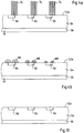
- the printing device includes a rotary roller 10 for holding a printing medium such as the paper web W.
- a pressure roller 12 is arranged parallel to the roller 10 in such a way that its cylindrical surface just touches the web W.
- an electronic print or write head 14 Around the pressure roller 12 are provided: an electronic print or write head 14, an ink application head 16 which offers the plate roller a dielectric, electrically uncharged ink, an ink transfer station 18 formed by the nip, and an erase head 22, all of which functions are controlled by a control device 24 .
- the control device 24 receives input signals in the form of a digital data stream for the gray or color values of an image to be reproduced. In the case of a color press, FIG.
- FIG. 1 represents a single printing unit for printing a single color component or signature of an original document, for example cyan component.
- three further printing units are arranged behind the roller 12 for printing the other color components, namely magenta, yellow and black, as for example in the U.S. Patent 4,792,860, the contents of which are hereby incorporated by reference.
- the device according to FIG. 1 print all four color signatures with modification for a multicolor application station, as described, for example, in US Pat. No. 5,325,120.
- the data representing the different color components of a color original are fed to the device in the form of successive streams (chains).
- the system can receive the data in the order of cyan, magenta, yellow, and black.
- a mass storage device 24a is preferably used in connection with the control device 24 for storing the relatively large amounts of data that are required to operate the device.
- the control device 24 controls the print head 14 such that when the print roller 12 rotates, the print head records electrostatic images on the roller surface 12a in accordance with at least one of the color components, as shown in the incoming data stream.
- the printhead can be a microtunnel head as specified in U.S. Patent 5,325,120.
- the application head 16 can be constructed like that described in the patent specification 4,792,860 or 5,325,120. It provides a melted thermoplastic ink made from pigment particles in one of the four inks dispersed in a binder.
- the platen surface 12a is preferably weakly color phobic so that the ink does not tend to adhere to the surface of the platen except at the locations charged by the printhead 14. If, for example, a cyan image is written on the printing roller 12, the application head 16 supplies cyan ink. Then, when the electrostatic image on the roller surface 12a has passed the application head 16, cyan ink is picked up by the head 16 at the charged areas of this image, and thereby a cyan image is developed on the platen surface 12a. As described in the aforementioned patents, the roller 12 is heated so that the ink remains melted on the surface 12a and adheres to the surface of the charged areas mentioned.
- the amounts of ink picked up or detected by the charged areas on the roller surface 12a increase monotonically with the field strengths emanating from these charged areas. This variation of field strengths across the image on the printing roller surface 12a facilitates the reproduction of the complete gray scale area. If the roller 26 rotates further, the developed area of the image is transported on the surface 12a to the application station 18, which consists of the gap between the rollers or cylinders 10 and 12.
- the control device 24 controls the position of the image on the roller 12 so that after this image has been developed and transported through the nip, the image developed thereon is transferred to the correct position on the web W.
- the device according to FIG. 1 differs from the devices described in the above patents in that its platen roller 12 has an anisotropic recording surface so that the electrical charges caused by the printhead 16 during a write operation are unevenly distributed on the platen surface 12a to thereby produce uneven electric fields that extend beyond the surface of the roller.
- the platen roller 12 is rotated so that these unevenly charged areas face the applicator head 16, the charged areas pick up ink from the applicator head by dielectrophoresis.
- roller 12 includes a rigid core 32, which may be made of steel or aluminum, and this core is preferably slotted as shown to reduce its weight and thereby allow air to cool through the core can circulate.
- a sleeve 34 is arranged around the core 32, for example made of a material such as ceramic material, which is thermally and electrically well insulated.
- a thin layer 38 for example 1 ⁇ m thick, is provided around the layer 36 and consists of a dielectric, for example silicon nitride or sapphire with a very high specific resistance.
- Layer 38 is anisotropic by providing a pattern of conductive points 42 in layer 38 that are electrically connected to conductive layer 36.
- the grounded dots can be formed, for example, by forming a pattern of minute through holes in the layer 38 in the thickness direction and filling the holes with conductive material such as metal or polysilicon.
- these points 42 in the figures of the drawings are shown relatively large and at a large distance. In reality, however, the points can never have a diameter of less than 1 ⁇ m and are only a few ⁇ m apart. As the FIG.
- the points 42 in the roller 12 are arranged at right angles in columns and rows, for example 10 ⁇ 10 points per picture element (pixel). However, it is obvious that other patterns can also be used.
- the dot pattern for each picture element (pixel) should be periodic for best results.
- the roller 12 is preferably also provided with a very thin outer coating 44 made of an adhesive material such as polytetrafluoroethylene (Teflon) or others that are color phobic. This surface adhesion coating prevents ink from adhering to uncharged areas of roller surface 12a and also minimizes ink smear on that surface.
- Teflon polytetrafluoroethylene
- the incoming positive charges accumulate on the recording surface 12a of the roller 12 so that areas of charge are applied, each of which has a specific Coulomb charge density corresponding to the bias of the control electrode, if any, in connection with the corresponding micro tunnel.
- the plasma in the microtunnels can be caused to "exit" at the end of the microtunnels by appropriately increasing the tunnel currents.
- the plasma can be thought of as a gaseous "wire" that charges the dielectric surface to the plasma potential.
- these bias levels can be digitally adjusted so that the individual microtunnels are separately activated and controlled by the controller so that electrostatic images are generated from imagewise patterns of the charge on the roller surface 12a.
- a feature of this invention is that when roller 12 is written to by printhead 14, the surface of sheet 38 is passed unevenly through each micro-tunnel of the printhead. In particular, the presence of the grounded points 42 causes the surface tension of the roller to periodically decrease to zero volts.
- each picture element (pixel) of the electronic image on the platen 12 consists of a microscopic pattern of unevenly distributed charge areas, the uneven electric fields cause - so-called micro-fields - which extend outward from the roller surface 12a; but these charges are averaged across the picture element (pixel), so that macroscopically the charge is proportional to the gray or color value for the picture element (pixel) in question.
- the non-uniform electric field at each spot polarizes the development medium and causes ink particles to be drawn to roller surface 12a by dielectrophoresis in an amount that is monotonous with the charge of each Point increases.
- Printing ink does not adhere to uncharged areas of the roller surface 12a, in particular not because the adhesive layer 44 is present.
- Writing heads other than the micro tunnel writing head described above can also be used to apply charges to the dielectric surface, but the micro tunnel writing head is preferred when the dots are grounded, as shown in FIG. 2 shown. Note that the grounded points of FIG. 2 do not have to be directly grounded, rather it is sufficient to connect to the ground plane through materials with a lower resistance than the dielectric.
- the dots could also be embedded in the dielectric, as long as defined areas are formed on the recording surface, the potential of which is closer to the ground potential.
- ions or charges are applied to the dielectric surface and then migrate to earthed points
- a grounded layer can be provided beneath the dielectric material so that the dielectric material can be charged between the charged point and the grounded layer and how a capacitor works. The dot retains much of its charge when the printhead moves away from it.
- the dielectric material on the surface around the point remains approximately uncharged or only very weakly charged. Microfields are thus formed between the charged point and the uncharged dielectric on the surface.
- roller 52 has a core 32, a ceramic sleeve 34 and a conductive layer or ground plane 36.
- a dielectric layer 54 is formed with a pattern of conductive areas or points 56 on her. These points are not connected to the conductive layer 36.
- the dots may be embedded on the dielectric material 54 or, less preferably, entirely provided therein, but the recording surface should have areas with a higher conductivity than that of the normal dielectric layer 54, which can still hold a charge even if the Printhead moves away.
- the roller 52 can also have an outer adhesive coating 60, the surface of which represents the recording surface 52a of the roller 52.
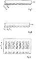
- FIGS. 4 and 5 show a print head 72 with a linear group of wire-like contacts or voltage feed points 74, which can run over the entire width of the printing roller.
- the contacts or voltage feed points 74 are "scratched" and the printhead 72 may be arranged so that the contacts resiliently abut the recording surface 52a of the platen 52 at locations of the conductive dots 56 thereon. Image-dependent voltages are then applied to the various contacts 74 when they face the conductive dots 56 so that the dots are charged.
- Each contact 74 can be quite small, for example several contacts within the width of a picture element (pixel), because only the corresponding point 56 has to be contacted very briefly (order of magnitude nanoseconds) in order for the conductive point to be fully charged to the full potential of the corresponding contact becomes.
- the contact can also be as wide as a picture element (pixel), and a single contact can also make contact with more than a single point.
- Conductive point 56 thus serves as one plate of a capacitor, ground plane 36 as the other. The dielectric between the point and the ground plane can thus be charged by the write head. When the write head moves away from the point, the dielectric material under the point and the connection point retain a charge, and thus field lines extend across the charged points and the substantially uncharged surrounding dielectric.
- microfields are formed that attract ink around the dots.
- the effectiveness of the printing roller is considerably increased by the presence of the points, because stronger fields can be generated than with wire-like contacts on a flat dielectric surface.
- the potential around each point is closer to the ground potential (desirable for creating strong cross fields) the thinner the dielectric layer 54 is.
- the roller 52 thus operates more or less the same as the roller 12 with regard to the detection of a pattern of electrical charge areas with microscopic periodic variation, but macroscopic image dependency.
- the charge areas thus produce non-uniform image-dependent electric fields that can and may extend from the roller surface 52a polarize a development medium and pull it onto this surface.
- the write head 72 with its "scratched" contacts 74 can be produced using the methods of conventional printed circuit board technology.
- the in FIG. 5 includes a substrate 76 made of an insulating material such as ceramic or glass, which extends over the full width of the printing roller 52.
- a selectively etchable insulating layer 78 made of silicon dioxide or the like is deposited on the substrate.
- a conductive metal layer 82 is deposited above this layer. The deposited metal can be patterned (ie etched after application of photoresist) so that a contact 74 is present approximately every 50 ⁇ m with suitable width / spacing dimensions. The distance can be, for example, one half of the metal width or can be chosen as desired.
- Terminal pads 74a may be provided at one end of the contacts for connecting the contacts to the pressure source, ie, a wire charging component. These paths can be shifted from one another as shown to provide enough space for wire bonding or to provide contact areas for a removable contact assembly (not shown). To "claw out” the working ends of the contacts 74, the layer 78 of insulating material at the bottom of the substrate 76 next to the contact working ends can be etched away so that the contact ends are free of the substrate and "float" as schematically shown in FIG. 4 shown.
- the conductive layer 82 can be formed as a bimetallic layer, so that when detached the metal bends off from the substrate like a bimetallic spring, so that the contacts 74 are in good elastic sliding contact with the roller surface 52 a.
- a write head By forming a write head as described, accurate spacing between contacts 74 of the write head is achieved.
- the ends of the contacts 74 can be made thicker for better wear resistance. You can also use these ends split to form a brush for better elasticity and better contact with the conductive dots on the platen.
- Each voltage feed point 74 can also be formed in the form of a plurality of smallest electrical fingers, as shown in FIG. 4a. In FIG. 4a, the points 56 are embedded in the dielectric layer 54.
- the electrical fingers of a single feed point 74 are all charged to an equal (similar) voltage, but have a very high resistivity in a direction parallel to a line immediately across the width of the recording surface.
- the control device for the write head can be set to the voltage of each feed point individually, as described above. Due to manufacturing tolerances, contact 74 may often touch not only the point but also part of the dielectric, as shown in FIG. 4a. But due to the larger difference and the lack of a conductive point that facilitates the feeding of the electrical charge, the charge on the dielectric on the surface is minimal. Thus, when voltage contact 74 moves away from the point, micro-fields arise between point 56, which remains charged, and the dielectric surface, which remains largely uncharged. It is also possible that the in FIG.
- the points shown contact the ground plane via resistors or ohmic connectors with a smaller specific resistance than that of the dielectric. If the feed points move away from the points, the point remains charged for a certain time, even if its discharge rate is higher than if there were no resistors.
- the optimal specific resistance between the point and the ground plane depends on various factors, including the speed of the printing roller, tension limits, desired ink strength and others. The specific resistance can also be via the Composition, depth and size of the points can be influenced.
- the points are preferably made of a hard metal compound, for example TiN, ZrN or zirconium oxide.
- FIG. 6 illustrates another embodiment of a pressure roller, generally designated 92, but having a slightly different anisotropic dielectric layer 94 on the conductive layer 38.
- the layer 94 also bears a pattern of conductive points 96.
- the points 96 are alternately connected to the ground plane 36 by conductive paths 98.
- the conductive paths 98 can be formed by "pinholes" filled with conductive material, by plated paths, or even by minute wires.
- conductive paths 98 may be made of a semiconductor material, such as polysilicon, so that there is a relatively high resistance. In this way, somewhat higher transverse electric fields are achieved over the recording surface 92 of the roller 92 when the roller is written with the write head 72. More specifically, even the polysilicon connection can be used directly as the conductive point 96; Covering with another, more conductive metal is not necessary because, from an electrostatic point of view, only very low conductances are required for points 96. The same applies to the points 42 on the roller 12 (FIG. 2). Another embodiment shown eliminates the need for a ground plane in the pressure roller because unearthed adjacent points of the dot pattern are charged in opposite directions. In FIG.
- FIG. 7 shows a write head 172 which has a multiplicity of sets S1, S2, S3 etc. of two feed points with a parallel arrangement to the direction of movement of a dielectric recording surface.
- the recording surface may be a simple dielectric surface, preferably one with dots or areas of higher conductivity on the surface as described above.
- the write head can be independently set to a voltage difference for each set S1, S2, etc. based on electronic data representing the image to be recorded on a dielectric recording surface.
- the voltage difference preferably varies between zero and a maximum of 30 to 200 volts, so that the ink is attracted variably in accordance with the voltage difference.
- FIG. 8 it is also possible to arrange the sets of voltage feeding points of the write head 172 in a direction perpendicular to the moving direction of the recording surface. The grouping can be done as for the write head of FIG. 4 and 5.
- the two FIGURES 7 and 8 there are also more than two Infeed points per set possible, e.g. three infeed points for one set with voltages V1, V2, V1.
- the voltages V1, V3, V1 can be such that the voltages of the feed points in the sets next to one another are equal. This helps to avoid microfields between two adjacent sets if desired.
- the recording surface for this embodiment can be a simple dielectric surface, and dots as described above can also be present.
- the points 156 can be formed as rectangles with the full size of a picture element (pixel), for example 50 micrometers.
- the varying voltages can be supplied by a DC voltage source.
- alternating voltage sources can also be used, the voltage amplitude being variable.
- an AC voltage source there is also the possibility of grounding the underlying layer of FIG. 3 as shown in FIG. 10 shown.
- the layer 136 is an ungrounded conductive layer which receives an approximately constant voltage equal to the mean value of the varying AC voltage when the pressure roller rotates.
- a printing component with a charged anisotropic surface can interact with a dielectric development medium or any other dielectric material with a dielectric constant greater than one.
- the term "printing ink” is therefore intended to generally refer to a dielectric development medium in which the dielectric constant is greater than one, and is not restricted to liquid printing inks.
- uncharged toners or printing inks charged ones can also be used in connection with the embodiments described above, but the resulting desired attraction of the color and the thicknesses must then be modified taking into account the stronger attraction.
- contact points may be used when charging the points or more conductive areas, instead of the wire contact points as shown in FIG. 4.
- the write head can also comprise a plasma charging component and charge via individual plasma introduction points, similar to the microtunnel plasma device described above.
- the print head can also have a gas charging device and charge the points via the gas delivery points.
- the contact wires of the embodiment shown in FIG. 4 can, for example, be designed such that there is no real contact with the recording surface, but rather the charges are conveyed via the air. It can thus be seen that the purposes described above are effectively achieved together with those arising from the above description. Certain changes can of course also be made to the above designs without departing from the scope of the invention. It is further assumed that the following claims are intended to cover all general and special features of the invention described here.
Landscapes
- Physics & Mathematics (AREA)
- General Physics & Mathematics (AREA)
- Printers Or Recording Devices Using Electromagnetic And Radiation Means (AREA)
- Dot-Matrix Printers And Others (AREA)
- Steering Control In Accordance With Driving Conditions (AREA)
- Auxiliary Devices For And Details Of Packaging Control (AREA)
- Electronic Switches (AREA)
Applications Claiming Priority (4)
| Application Number | Priority Date | Filing Date | Title |
|---|---|---|---|
| US342135 | 1989-04-24 | ||
| US34213594A | 1994-11-18 | 1994-11-18 | |
| US08/467,200 US5821973A (en) | 1994-11-18 | 1995-06-06 | Printing device and method |
| US467200 | 1999-12-20 |
Publications (3)
| Publication Number | Publication Date |
|---|---|
| EP0713154A2 true EP0713154A2 (fr) | 1996-05-22 |
| EP0713154A3 EP0713154A3 (fr) | 1997-06-04 |
| EP0713154B1 EP0713154B1 (fr) | 2001-03-07 |
Family
ID=26992841
Family Applications (1)
| Application Number | Title | Priority Date | Filing Date |
|---|---|---|---|
| EP95117917A Expired - Lifetime EP0713154B1 (fr) | 1994-11-18 | 1995-11-14 | Dispositif d'impression et méthode |
Country Status (6)
| Country | Link |
|---|---|
| US (1) | US5821973A (fr) |
| EP (1) | EP0713154B1 (fr) |
| JP (1) | JPH08241013A (fr) |
| CN (1) | CN1129174A (fr) |
| AT (1) | ATE199598T1 (fr) |
| DE (1) | DE59509075D1 (fr) |
Families Citing this family (1)
| Publication number | Priority date | Publication date | Assignee | Title |
|---|---|---|---|---|
| FR2878536B1 (fr) * | 2004-11-30 | 2007-04-06 | Analyses Mesures Pollutions A | Procede d'ennoblissement textile a la continue et installation mettant en oeuvre ledit procede |
Citations (4)
| Publication number | Priority date | Publication date | Assignee | Title |
|---|---|---|---|---|
| US3739748A (en) | 1970-12-15 | 1973-06-19 | Xerox Corp | Donor for touchdown development |
| US4792860A (en) | 1987-02-27 | 1988-12-20 | Kuehrle Manfred R | Thermodynamic printing method and means |
| US5315061A (en) | 1989-10-13 | 1994-05-24 | Ricoh Company, Ltd. | Developing apparatus using a developer carrier capable of forming microfields |
| US5325120A (en) | 1991-11-15 | 1994-06-28 | Kuehnle Manfred R | Electrostatic reproduction apparatus having a dielectric ink-phobic imaging member and field-emission write head |
Family Cites Families (13)
| Publication number | Priority date | Publication date | Assignee | Title |
|---|---|---|---|---|
| BE758652A (fr) * | 1969-11-07 | 1971-05-10 | Int Standard Electric Corp | Perfectionnements aux dispositifs d'impression |
| US3689933A (en) * | 1970-01-07 | 1972-09-05 | Energy Conversion Devices Inc | Apparatus employed in electrostatic printing |
| US3645618A (en) * | 1970-12-18 | 1972-02-29 | Xerox Corp | Vacuum nozzle to remove agglomerates on a toner applicator |
| US3759222A (en) * | 1971-03-04 | 1973-09-18 | Xerox Corp | Microfield donor with continuously reversing microfields |
| JPS6036396B2 (ja) * | 1979-11-20 | 1985-08-20 | 株式会社リコー | 静電記録用マルチスタイラスヘツド |
| JPS57168268A (en) * | 1981-04-09 | 1982-10-16 | Ricoh Co Ltd | Picture forming method |
| JPS61286162A (ja) * | 1985-06-14 | 1986-12-16 | Canon Inc | 静電記録ヘツド |
| US4862414A (en) * | 1986-06-11 | 1989-08-29 | Kuehnle Manfred R | Optoelectronic recording tape or strip comprising photoconductive layer on thin, monocrystalline, flexible sapphire base |
| US5029156A (en) * | 1987-05-11 | 1991-07-02 | Kuehnle Manfred R | Method and means for reading electronic signal patterns stored on a movable image recording surface |
| US4897731A (en) * | 1987-05-11 | 1990-01-30 | Xmx Corp. | Method and means for reading electronic signal patterns stored on a movable image recording surface |
| US5103263A (en) * | 1989-05-23 | 1992-04-07 | Delphax Systems | Powder transport, fusing and imaging apparatus |
| US5063538A (en) * | 1989-08-30 | 1991-11-05 | Kuehnle Manfred R | Optoelectronic signal recording medium and method of making same |
| IL103705A (en) * | 1991-11-15 | 1995-12-08 | Kuehnle Manfred R | Electro-thermal printing ink and method and printing device with its help |
-
1995
- 1995-06-06 US US08/467,200 patent/US5821973A/en not_active Expired - Lifetime
- 1995-11-14 AT AT95117917T patent/ATE199598T1/de not_active IP Right Cessation
- 1995-11-14 DE DE59509075T patent/DE59509075D1/de not_active Expired - Fee Related
- 1995-11-14 EP EP95117917A patent/EP0713154B1/fr not_active Expired - Lifetime
- 1995-11-17 CN CN95117540A patent/CN1129174A/zh active Pending
- 1995-11-17 JP JP7299732A patent/JPH08241013A/ja active Pending
Patent Citations (4)
| Publication number | Priority date | Publication date | Assignee | Title |
|---|---|---|---|---|
| US3739748A (en) | 1970-12-15 | 1973-06-19 | Xerox Corp | Donor for touchdown development |
| US4792860A (en) | 1987-02-27 | 1988-12-20 | Kuehrle Manfred R | Thermodynamic printing method and means |
| US5315061A (en) | 1989-10-13 | 1994-05-24 | Ricoh Company, Ltd. | Developing apparatus using a developer carrier capable of forming microfields |
| US5325120A (en) | 1991-11-15 | 1994-06-28 | Kuehnle Manfred R | Electrostatic reproduction apparatus having a dielectric ink-phobic imaging member and field-emission write head |
Also Published As
| Publication number | Publication date |
|---|---|
| ATE199598T1 (de) | 2001-03-15 |
| DE59509075D1 (de) | 2001-04-12 |
| CN1129174A (zh) | 1996-08-21 |
| US5821973A (en) | 1998-10-13 |
| EP0713154A3 (fr) | 1997-06-04 |
| JPH08241013A (ja) | 1996-09-17 |
| EP0713154B1 (fr) | 2001-03-07 |
Similar Documents
| Publication | Publication Date | Title |
|---|---|---|
| DE69231341T2 (de) | Bilderzeugungsgerät | |
| DE3411948C2 (fr) | ||
| DE69512643T2 (de) | Tonerprojektionsdrucker mit Mitteln um die Tonerverstreuung zu reduzieren | |
| DE2419595C2 (de) | Elektrographisches Aufzeichnungsverfahren | |
| DE69224912T2 (de) | Verfahren zum elektronischen drucken | |
| DE3884814T2 (de) | Verfahren zur herstellung eines latenten elektrischen ladungsmusters und anordnung dazu. | |
| DE10242972A1 (de) | Tintenstrahlverfahren mit Entfernung überschüssiger Flüssigkeit aus einem Zwischenelement | |
| EP0713155B1 (fr) | Dispositif d'impression | |
| DE19703187A1 (de) | Elektrostatisches Druckverfahren und Vorrichtung mit einem Kontaktborsten enthaltenden Bebilderungskopf | |
| DE60107913T2 (de) | Bilderzeugungsgerät | |
| DE2755489A1 (de) | Verfahren und vorrichtung zur elektrostatischen uebertragung | |
| EP0713154B1 (fr) | Dispositif d'impression et méthode | |
| DE4038085C2 (de) | Drucker mit direkter elektrostatischer Tonerbilderzeugung | |
| DE69517967T2 (de) | Tonerprojektionsdrucker mit verbesserter Steuerelektrodenstruktur | |
| DE60309951T2 (de) | Schreibkopf und damit versehenes Bilderzeugungsgerät | |
| EP0508273A1 (fr) | Dispositif d'impression pour imprimer en offset avec un toner | |
| DE69703522T2 (de) | Bilderzeugungsgerät | |
| DE2842823A1 (de) | Elektrographisches drucksystem | |
| DE69515167T2 (de) | Feldeffekt tonungs-verfahren/vorrichtung | |
| DE69700075T2 (de) | Vorrichtung zum direkten elektrostatischen Drucken (DEP) mit konstantem Abstand zwischen der Druckkopfstruktur und den Tonerzufuhrmitteln | |
| DE69514505T2 (de) | Tonerprojektionsdrucker mit kapazitivgekoppelter Steuerelektrodenstruktur | |
| DE69728248T2 (de) | Tonerprojektionssystem | |
| EP0779560B1 (fr) | Procédé et appareil de développement d'une imgae latente électrostatique | |
| DE19623132A1 (de) | Drucken mit direktem Tonerauswurf unter Verwendung eines Zwischentransfermediums | |
| DE10030166A1 (de) | Verfahren zum Reinigen eines elektrografischen Schreibkopfes und Vorrichtung zum Erzeugen eines elektrostatischen Musters |
Legal Events
| Date | Code | Title | Description |
|---|---|---|---|
| PUAI | Public reference made under article 153(3) epc to a published international application that has entered the european phase |
Free format text: ORIGINAL CODE: 0009012 |
|
| 17P | Request for examination filed |
Effective date: 19951114 |
|
| AK | Designated contracting states |
Kind code of ref document: A2 Designated state(s): AT DE ES FR GB IT NL SE |
|
| PUAL | Search report despatched |
Free format text: ORIGINAL CODE: 0009013 |
|
| AK | Designated contracting states |
Kind code of ref document: A3 Designated state(s): AT DE ES FR GB IT NL SE |
|
| 17Q | First examination report despatched |
Effective date: 19981210 |
|
| GRAG | Despatch of communication of intention to grant |
Free format text: ORIGINAL CODE: EPIDOS AGRA |
|
| GRAG | Despatch of communication of intention to grant |
Free format text: ORIGINAL CODE: EPIDOS AGRA |
|
| GRAH | Despatch of communication of intention to grant a patent |
Free format text: ORIGINAL CODE: EPIDOS IGRA |
|
| GRAH | Despatch of communication of intention to grant a patent |
Free format text: ORIGINAL CODE: EPIDOS IGRA |
|
| GRAA | (expected) grant |
Free format text: ORIGINAL CODE: 0009210 |
|
| AK | Designated contracting states |
Kind code of ref document: B1 Designated state(s): AT DE ES FR GB IT NL SE |
|
| PG25 | Lapsed in a contracting state [announced via postgrant information from national office to epo] |
Ref country code: IT Free format text: LAPSE BECAUSE OF FAILURE TO SUBMIT A TRANSLATION OF THE DESCRIPTION OR TO PAY THE FEE WITHIN THE PRESCRIBED TIME-LIMIT;WARNING: LAPSES OF ITALIAN PATENTS WITH EFFECTIVE DATE BEFORE 2007 MAY HAVE OCCURRED AT ANY TIME BEFORE 2007. THE CORRECT EFFECTIVE DATE MAY BE DIFFERENT FROM THE ONE RECORDED. Effective date: 20010307 Ref country code: ES Free format text: THE PATENT HAS BEEN ANNULLED BY A DECISION OF A NATIONAL AUTHORITY Effective date: 20010307 |
|
| REF | Corresponds to: |
Ref document number: 199598 Country of ref document: AT Date of ref document: 20010315 Kind code of ref document: T |
|
| REF | Corresponds to: |
Ref document number: 59509075 Country of ref document: DE Date of ref document: 20010412 |
|
| GBT | Gb: translation of ep patent filed (gb section 77(6)(a)/1977) |
Effective date: 20010430 |
|
| PG25 | Lapsed in a contracting state [announced via postgrant information from national office to epo] |
Ref country code: SE Free format text: LAPSE BECAUSE OF FAILURE TO SUBMIT A TRANSLATION OF THE DESCRIPTION OR TO PAY THE FEE WITHIN THE PRESCRIBED TIME-LIMIT Effective date: 20010607 |
|
| ET | Fr: translation filed | ||
| PG25 | Lapsed in a contracting state [announced via postgrant information from national office to epo] |
Ref country code: AT Free format text: LAPSE BECAUSE OF NON-PAYMENT OF DUE FEES Effective date: 20011114 |
|
| PGFP | Annual fee paid to national office [announced via postgrant information from national office to epo] |
Ref country code: FR Payment date: 20011122 Year of fee payment: 7 |
|
| PGFP | Annual fee paid to national office [announced via postgrant information from national office to epo] |
Ref country code: NL Payment date: 20011127 Year of fee payment: 7 |
|
| REG | Reference to a national code |
Ref country code: GB Ref legal event code: IF02 |
|
| PLBE | No opposition filed within time limit |
Free format text: ORIGINAL CODE: 0009261 |
|
| STAA | Information on the status of an ep patent application or granted ep patent |
Free format text: STATUS: NO OPPOSITION FILED WITHIN TIME LIMIT |
|
| 26N | No opposition filed | ||
| PGFP | Annual fee paid to national office [announced via postgrant information from national office to epo] |
Ref country code: GB Payment date: 20021021 Year of fee payment: 8 |
|
| PG25 | Lapsed in a contracting state [announced via postgrant information from national office to epo] |
Ref country code: NL Free format text: LAPSE BECAUSE OF NON-PAYMENT OF DUE FEES Effective date: 20030601 |
|
| PG25 | Lapsed in a contracting state [announced via postgrant information from national office to epo] |
Ref country code: FR Free format text: LAPSE BECAUSE OF NON-PAYMENT OF DUE FEES Effective date: 20030731 |
|
| NLV4 | Nl: lapsed or anulled due to non-payment of the annual fee |
Effective date: 20030601 |
|
| REG | Reference to a national code |
Ref country code: FR Ref legal event code: ST |
|
| PG25 | Lapsed in a contracting state [announced via postgrant information from national office to epo] |
Ref country code: GB Free format text: LAPSE BECAUSE OF NON-PAYMENT OF DUE FEES Effective date: 20031114 |
|
| GBPC | Gb: european patent ceased through non-payment of renewal fee |
Effective date: 20031114 |
|
| PGFP | Annual fee paid to national office [announced via postgrant information from national office to epo] |
Ref country code: DE Payment date: 20041124 Year of fee payment: 10 |
|
| PG25 | Lapsed in a contracting state [announced via postgrant information from national office to epo] |
Ref country code: DE Free format text: LAPSE BECAUSE OF NON-PAYMENT OF DUE FEES Effective date: 20060601 |