EP0713248A2 - Procédé de moulage et appareil - Google Patents
Procédé de moulage et appareil Download PDFInfo
- Publication number
- EP0713248A2 EP0713248A2 EP95307982A EP95307982A EP0713248A2 EP 0713248 A2 EP0713248 A2 EP 0713248A2 EP 95307982 A EP95307982 A EP 95307982A EP 95307982 A EP95307982 A EP 95307982A EP 0713248 A2 EP0713248 A2 EP 0713248A2
- Authority
- EP
- European Patent Office
- Prior art keywords
- resin
- dies
- mold
- die
- portions
- Prior art date
- Legal status (The legal status is an assumption and is not a legal conclusion. Google has not performed a legal analysis and makes no representation as to the accuracy of the status listed.)
- Withdrawn
Links
Images










Classifications
-
- B—PERFORMING OPERATIONS; TRANSPORTING
- B29—WORKING OF PLASTICS; WORKING OF SUBSTANCES IN A PLASTIC STATE IN GENERAL
- B29C—SHAPING OR JOINING OF PLASTICS; SHAPING OF MATERIAL IN A PLASTIC STATE, NOT OTHERWISE PROVIDED FOR; AFTER-TREATMENT OF THE SHAPED PRODUCTS, e.g. REPAIRING
- B29C45/00—Injection moulding, i.e. forcing the required volume of moulding material through a nozzle into a closed mould; Apparatus therefor
- B29C45/14—Injection moulding, i.e. forcing the required volume of moulding material through a nozzle into a closed mould; Apparatus therefor incorporating preformed parts or layers, e.g. injection moulding around inserts or for coating articles
- B29C45/14639—Injection moulding, i.e. forcing the required volume of moulding material through a nozzle into a closed mould; Apparatus therefor incorporating preformed parts or layers, e.g. injection moulding around inserts or for coating articles for obtaining an insulating effect, e.g. for electrical components
- B29C45/14655—Injection moulding, i.e. forcing the required volume of moulding material through a nozzle into a closed mould; Apparatus therefor incorporating preformed parts or layers, e.g. injection moulding around inserts or for coating articles for obtaining an insulating effect, e.g. for electrical components connected to or mounted on a carrier, e.g. lead frame
-
- H—ELECTRICITY
- H10—SEMICONDUCTOR DEVICES; ELECTRIC SOLID-STATE DEVICES NOT OTHERWISE PROVIDED FOR
- H10W—GENERIC PACKAGES, INTERCONNECTIONS, CONNECTORS OR OTHER CONSTRUCTIONAL DETAILS OF DEVICES COVERED BY CLASS H10
- H10W74/00—Encapsulations, e.g. protective coatings
- H10W74/01—Manufacture or treatment
-
- B—PERFORMING OPERATIONS; TRANSPORTING
- B29—WORKING OF PLASTICS; WORKING OF SUBSTANCES IN A PLASTIC STATE IN GENERAL
- B29C—SHAPING OR JOINING OF PLASTICS; SHAPING OF MATERIAL IN A PLASTIC STATE, NOT OTHERWISE PROVIDED FOR; AFTER-TREATMENT OF THE SHAPED PRODUCTS, e.g. REPAIRING
- B29C45/00—Injection moulding, i.e. forcing the required volume of moulding material through a nozzle into a closed mould; Apparatus therefor
- B29C45/17—Component parts, details or accessories; Auxiliary operations
- B29C45/26—Moulds
- B29C45/34—Moulds having venting means
- B29C45/345—Moulds having venting means using a porous mould wall or a part thereof, e.g. made of sintered metal
-
- H—ELECTRICITY
- H10—SEMICONDUCTOR DEVICES; ELECTRIC SOLID-STATE DEVICES NOT OTHERWISE PROVIDED FOR
- H10W—GENERIC PACKAGES, INTERCONNECTIONS, CONNECTORS OR OTHER CONSTRUCTIONAL DETAILS OF DEVICES COVERED BY CLASS H10
- H10W74/00—Encapsulations, e.g. protective coatings
- H10W74/01—Manufacture or treatment
- H10W74/016—Manufacture or treatment using moulds
-
- B—PERFORMING OPERATIONS; TRANSPORTING
- B29—WORKING OF PLASTICS; WORKING OF SUBSTANCES IN A PLASTIC STATE IN GENERAL
- B29C—SHAPING OR JOINING OF PLASTICS; SHAPING OF MATERIAL IN A PLASTIC STATE, NOT OTHERWISE PROVIDED FOR; AFTER-TREATMENT OF THE SHAPED PRODUCTS, e.g. REPAIRING
- B29C45/00—Injection moulding, i.e. forcing the required volume of moulding material through a nozzle into a closed mould; Apparatus therefor
- B29C45/14—Injection moulding, i.e. forcing the required volume of moulding material through a nozzle into a closed mould; Apparatus therefor incorporating preformed parts or layers, e.g. injection moulding around inserts or for coating articles
- B29C45/14639—Injection moulding, i.e. forcing the required volume of moulding material through a nozzle into a closed mould; Apparatus therefor incorporating preformed parts or layers, e.g. injection moulding around inserts or for coating articles for obtaining an insulating effect, e.g. for electrical components
- B29C45/14655—Injection moulding, i.e. forcing the required volume of moulding material through a nozzle into a closed mould; Apparatus therefor incorporating preformed parts or layers, e.g. injection moulding around inserts or for coating articles for obtaining an insulating effect, e.g. for electrical components connected to or mounted on a carrier, e.g. lead frame
- B29C2045/14663—Injection moulding, i.e. forcing the required volume of moulding material through a nozzle into a closed mould; Apparatus therefor incorporating preformed parts or layers, e.g. injection moulding around inserts or for coating articles for obtaining an insulating effect, e.g. for electrical components connected to or mounted on a carrier, e.g. lead frame the mould cavity walls being lined with a film, e.g. release film
-
- H—ELECTRICITY
- H10—SEMICONDUCTOR DEVICES; ELECTRIC SOLID-STATE DEVICES NOT OTHERWISE PROVIDED FOR
- H10W—GENERIC PACKAGES, INTERCONNECTIONS, CONNECTORS OR OTHER CONSTRUCTIONAL DETAILS OF DEVICES COVERED BY CLASS H10
- H10W72/00—Interconnections or connectors in packages
- H10W72/851—Dispositions of multiple connectors or interconnections
- H10W72/874—On different surfaces
- H10W72/884—Die-attach connectors and bond wires
-
- H—ELECTRICITY
- H10—SEMICONDUCTOR DEVICES; ELECTRIC SOLID-STATE DEVICES NOT OTHERWISE PROVIDED FOR
- H10W—GENERIC PACKAGES, INTERCONNECTIONS, CONNECTORS OR OTHER CONSTRUCTIONAL DETAILS OF DEVICES COVERED BY CLASS H10
- H10W90/00—Package configurations
- H10W90/701—Package configurations characterised by the relative positions of pads or connectors relative to package parts
- H10W90/731—Package configurations characterised by the relative positions of pads or connectors relative to package parts of die-attach connectors
- H10W90/736—Package configurations characterised by the relative positions of pads or connectors relative to package parts of die-attach connectors between a chip and a stacked lead frame, conducting package substrate or heat sink
-
- H—ELECTRICITY
- H10—SEMICONDUCTOR DEVICES; ELECTRIC SOLID-STATE DEVICES NOT OTHERWISE PROVIDED FOR
- H10W—GENERIC PACKAGES, INTERCONNECTIONS, CONNECTORS OR OTHER CONSTRUCTIONAL DETAILS OF DEVICES COVERED BY CLASS H10
- H10W90/00—Package configurations
- H10W90/701—Package configurations characterised by the relative positions of pads or connectors relative to package parts
- H10W90/751—Package configurations characterised by the relative positions of pads or connectors relative to package parts of bond wires
- H10W90/756—Package configurations characterised by the relative positions of pads or connectors relative to package parts of bond wires between a chip and a stacked lead frame, conducting package substrate or heat sink
Definitions
- the present invention relates to a method and an apparatus for manufacturing a semiconductor integrated circuit device which method and apparatus contain a molding process for sealing a semiconductor chip with mold resin, and more particularly to a technique that may effectively apply to a transfer molding technique provided in the molding apparatus for manufacturing a semiconductor chip.
- a resin molding apparatus that is, a molding apparatus a resin-sealed semiconductor IC device in which a semiconductor chip or a pellet is sealed by a heat-hardening mold resin such as a QFP (Quad Flat Package) type semiconductor IC device
- the currently used apparatus is such as disclosed in J-P-A 52-95765.
- a molding process is provided for manufacturing a resin-sealed semiconductor device having a DIP (Dual In-Line Package) or a QFP (Quad Flat Package) structure.
- a part of a lead frame is sealed by a transfer molding apparatus, and its relevant parts such as a semiconductor chip, wires and the inner ends of the lead are covered by a sealing material such as resin.
- the transfer molding apparatus is located on a conveying path of a lead frame between a loader and an unloader. After a semiconductor chip is bonded on the lead frame, the loader serves to put the lead frame into the transfer molding apparatus, in which a package is formed on the lead frame. Then, the resulting semiconductor chip is sealed with resin. The lead frame having the package formed thereon is taken out of the molding apparatus and then is put into the unloader.
- the molding apparatus has an upper die and a lower one for forming mold cavities when these dies are matched with each other. Within each mold cavity is located a lead frame having plural semiconductor chips fixed thereon. In this state, molten resin is filled in the mold cavity. The molten resin is flown from a pot formed in the die to the cavity through runners and resin gates.
- the molding apparatus provides an air vent for preventing some shortcomings such as air inclusion and resin shortage, which may appear when the resin is filled in the cavity, at each corner of each cavity portion except the resin gate. Especially, this air vent is intended for completely filling the mold resin in the cavities. Air left in each cavity is discharged from the air vent to the outside. After the resin implanted into the cavity is hardened, that is, a mold is formed, to take out the mold form from the die, the die provides ejector pins. Each ejector pin is projected into the cavity for separating from the dies the lead frame having culls and molded portion corresponding to runners and resin gates.
- the transfer molding apparatus is described in "VLSI Packaging Technique (Last Volume)" Nikkei BP.edition, May 15, 1993, pages 34 to 40, for example.
- This publication describes that the upper and the lower dies provide the corresponding heaters.
- the upper die is supported by a movable panel that is vertically moved along a guide and is fitted to the lower die for mold clamping.
- the publication also has a chart illustrating a molding routine. In the chart, the lead frame is placed on the lower die and the upper die (mould) is pressed down onto the lower die for mold clamping. Then, a preliminary heated tablet is put into a pot.
- the tablet is molten in the pot through the effect of a heater.
- the molten resin is filled into the cavity under the pressure given by a plunger. Air left in the cavity is discharged out through the air vent.
- Japanese Unexamined Laid-open No. 62-135330 also discloses a method for forming a mold. This method uses a die formed so that porous metal tips are inserted in continuous pores formed in the cavity. When the mold is separated from the die, gas is supplied from the outside through the metal tips.
- the Japanese Unexamined Laid-open No. Hei 5-74827 discloses a metallic die having ejector pins each formed of porous metal.
- the resin flowing at a faster pace reaches the air vent and blocks the air vent.
- the air left in the cavity is disallowed to be discharged out of the die, that is, confined in the cavity.
- the application of an implanting pressure to the air-included resin reduces a volume of the left air but may bring about foams or sinks in the package. They may be adverse factors and lower reliability of quality of the package.
- the resin is leaked by the implanting pressure applied from the air vent, leaked resin adheres to the lead frame or the air vent as flash.
- the flash on the lead frame is may be dropped when cutting or bending the lead frame in the later process. The dropped flash may impair the package.
- the air vent is clogged. This may bring about defective resin filling when molding the package.
- the die for separating the molded product from the metallic die, in other words, taking the product out of the die, the die contains plural ejector pins, so that the die may be so complicated. To design and manufacture the die, a lot of time and cost are required.
- concave portions may be formed on the surface of the molded product. Those concave portions may be defective portions such as chip cracks or package slits.
- the conventional transfer molding apparatus is arranged to discharge the air left inside of the cavity out of the air vent. Hence, a small amount of resin is leaked to the air vent with the air.
- the resin hardened in the air vent is so thin that it may be easily chipped. In the cutting process subsequent to the sealing process, if the resin is chipped and dropped onto the cutting die, the chipped resin may impair or transform the outer lead.
- the adhesive resin is accumulated in the air vent so that the accumulated resin may clog the air vent. This may bring about shortage of filling resin in the cavity. This shortage of filling resin may bring about foams (voids) and sinks, which result in lowering the quality of the molded product (semiconductor device).
- the mold in the die for forming the thin product (semiconductor device), when separating the molded semiconductor device containing culls and the corresponding portions to the runners and the gates from the dies with the ejector pints, the mold (resin package) is pricked by the ejector pins. This pricking bring about concave portions on the surface of the mold or may sometimes bring about chip cracks or package slits.
- the die For preventing the voids, the die provides over-runners, dummy cavities, air vents, flow cavities and ejector pins for thrusting the molded product (semiconductor device) from the cavities.
- the die pattern is so complicated that it needs a lot of time and cost for its design and manufacture.
- a method for manufacturing a semiconductor integrated circuit includes a step of preparing a chip-lead compound made of a lead frame or a thin wired sheet containing plural semiconductor chips and plural inner leads directly or indirectly electrically coupled on an electrode formed on a first main face of each of those chips; a step of locating the chip-lead compound between a first die and a second die in the molding apparatus made of a porous material and having the first die and the second die for forming plural mold cavities for sealing the semiconductor chips in concert with the first die, in which at least one portion of the inner surface of the mold cavity of at least one of the first and the second dies serves to inhibit intrusion of the mold resin down to a predetermined depth and pass at least part of gas components for preventing occurrence of voids; a step of pressing both of the dies against each other in the state of locating the chip-lead compound between the upper and the lower dies; a step of exposing the mold cavity formed by the clamped dies toward the atmosphere through the portion made
- the chip-lead compound is separated from the dies by injecting gas into the mold cavities through the portion made of the porous material.
- the gas When the mold resin is injected to the mold cavities, the gas may be sucked and discharged from the mold cavities into the outside.
- the method for manufacturing a semiconductor integrated circuit device includes the step of discharging out the gas left in the mold cavities through air vents made of the porous material forming at least one of these two dies when implanting the molten resin in the mold cavities formed by these dies in the state of contacting the first die with the second die.
- the method for manufacturing a semiconductor integrated circuit device includes the step of locating the chip-lead compound between the first die and the second die in the molding apparatus having the first die and the second die for forming plural mold cavities for sealing plural semiconductor chips in concert with the first die, in which apparatus the almost of the surface of each mold cavity is formed of a porous material and serves to inhibit intrusion of the mold resin to a predetermined depth and at least part of gas components are allowed to pass through the porous material, for preventing occurrence of voids.
- the method for manufacturing a semiconductor integrated circuit device includes the step of locating the chip-lead compound between the first and the second dies in the molding apparatus having the first die, the second die designed to have plural mold cavities for sealing plural semiconductor chips together with the first die, in which apparatus at least an opposite portion to each inside of those mold cavities to a gate is formed of a porous material and serves to inhibit intrusion of the mold resin down to a predetermined depth and at least part of gas components are allowed to pass through the porous material, for preventing occurrence of voids.
- the method for manufacturing a semiconductor integrated circuit device includes the step of locating the chip-lead compound between the first die and the second die in the molding apparatus having the first die and the second die designed to have plural mold cavities for sealing plural semiconductor chips together with the first die, one or more pots for accommodating one or more resin tables, and one or more runners for connecting them, in which apparatus at least part of each inside of the pots, the runners and at least part of an inside of a plunger slidably provided in each of the pots serve to inhibit intrusion of the mold resin down to a predetermined depth and at least part of gas components are allowed to pass through the porous material, for preventing occurrence of voids.
- the method for manufacturing a semiconductor integrated circuit includes the step of inserting a resin tablet to a resin tablet inserting portion provided in the lower die through a space between the upper die and the lower die in the molding apparatus having the upper die and the lower die designed to have plural mold cavities for sealing plural semiconductor chips, plural pots for accommodating resin tables for a predetermined number of mold cavities, respectively, and plural runners for connecting them, in which apparatus at least part of each inside of the mold cavities, the pots, and the runners are formed of a porous material and serves to inhibit intrusion of the mold resin down to a predetermined depth, for preventing occurrence of the mold resin.
- the method for manufacturing a semiconductor integrated circuit device includes the step of separating the sealed chip-lead compound from at least one of the first and the second dies by separating the first die from the second die as gas is being injected to the mold cavity through a porous material after the mold resin is implanted to the mold cavity, and is executed to manufacture a thin resin sealed semiconductor integrated circuit device whose characteristic is degraded by physical transformation of the sealing portion if the sealing portion is separated by the ejector pins provided in the molding apparatus.
- the method for manufacturing a semiconductor integrated circuit device includes the step of implanting molten mold resin to the mold cavities formed by the first and the second dies and discharging only gas in the mold cavities in the state of clamping the first and the second dies with each other, the first die having a main body with ventilating portions made of a porous material and having air vents and a filter layer formed on the surface of the main body and having pores communicating with the air vents, inhibiting inflow of mold resin molecules to the pores and allowing only the flow of gas, the communicating pores having smaller inner diameters than the air vents.
- a molding apparatus includes a first die, a second die designed to relatively come closer to or off the first die and have mold cavities formed to correspond to packages in concert with the first die, at least one of the first and the second dies having a main body formed to contain a ventilating portion made of a porous material and having air vents, the surface of the ventilating portion having a filter layer containing pores communicating with the air vents, the communicating pores serving to inhibit inflow of mold resin to the air vents and allowing flow of only gas into the air vents.
- a molding apparatus includes a first die, a second die designed to relatively move closer to or off the first die and form mold cavities suited to correspond to packages in concert with the first die, at least one of the first and the second dies being formed of a main body providing a ventilating portion made of a porous material and having air vents and a fine porous portion buried to a predetermined depth from the inner surface of each mold cavity and formed to have communicating pores containing smaller inner diameters than the air vents, those communicating pores for preventing intrusion of mold resin and allowing passage of at least part of gas components.
- a coating layer may be formed on the surface of the fine porous portion.
- the molding apparatus of the invention enables to manufacture a semiconductor integrated circuit device having a high-quality resin sealing portion with no foams and sinks left in the cavities.
- the gas left in the mold cavities may be discharged out of the whole or the part of each mold cavity.
- gas such as air left in the pot or the runner may be discharged out while the mold resin is guided from the pot to the corresponding mold cavity.
- the gas is injected from the outside to the cavity.
- the chip-lead compound is allowed to be taken out without having to use the ejector pins.
- a high-quality device may be manufactured without having to physically transform the sealing portion.
- a filter layer On the surface of the main body of the die made of a porous material, a filter layer is formed.
- This filter layer provides pores communicating with air vents and having a smaller diameter than the air vents. Hence, the filter layer serves to positively prevent inflow of the mold resin to the air vents.
- the fine porous medium is buried into a predetermined depth of each communicating pore, it is possible to positively prevent inflow of the mold resin into the air vents.
- Fig. 1 is a perspective view showing an outer appearance of the overall transfer molding apparatus used for the method for manufacturing a semiconductor integrated circuit device according to the present invention.
- This apparatus is used for sealing a semiconductor chip of a semiconductor pellet, that is, a lead frame having the semiconductor chip bonded thereon, with resin.
- the lead frame having the semiconductor chip bonded thereon is conveyed from a loader 7 to the transfer molding apparatus 8, in which the semiconductor chip is sealed. After the lead frame is packaged with resin, the packaged lead frame is conveyed out and then accommodated by an unloader 9.
- a numeral 10 denotes a pedestal.
- a numeral 11 denotes columns whose lower ends are secured on the pedestal 10.
- 12 denotes a fixed platen secured on the upper ends of the columns 11.
- a movable platen 13 is fitted to the columns 11.
- the movable platen 13 is allowed to be vertically moved as guided by the columns 11.
- the movable platen 13 provides a driving block 14 secured thereon.
- the driving block 14 is linked to a rod 16 of a cylinder 15 located on the pedestal 10.
- the cylinder 15 is operated by oil or air pressure.
- the movable platen 13 is vertically moved through the effect of the driving block 14 operated by the cylinder 15.
- the fixed platen 12 is fixed with an upper unit 21, that is, an upper molding die unit, the die matching face 21a of which is directed downward.
- a lower unit 22, that is, a lower molding die unit is secured on the movable platen 13.
- the lower unit 22 has a die matching face 22a directed upward.
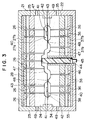
- the details of the upper unit 21 and the lower unit 22 will be illustrated in Figs. 3 and 4.
- the upper unit 21 is made of metal such as steel and has a boxy protecting frame 23 whose lower portion is opened.
- a numeral 24 denotes a die body served as a first die, which is fitted to the protecting frame 23.
- a numeral 25 denotes a protecting plate secured on the inside of the die body 24.
- Plural ejector pins 26 are axially penetrated through the die body 24 and the protecting plate 25. Those ejector pins 26 are allowed to slidably travel therethrough. Each base end of the ejector pins 26 is pressed between a first ejector plate 27a and a second ejector plate 27b secured thereon.
- a gap 28 is formed between the ejector plate 27b and the protecting plate 25, a gap 28 is formed. In the range of the gap 28, the ejector plates 27a and 27b are allowed to vertically move against the die body 24. The vertical action of the ejector plates 27a and 27b leads to that of the ejector pins 26.
- the lower unit 22 is made of metal such as steel.
- the lower unit 22 has a boxy protecting frame 33 whose top is opened. This protecting frame 33 is fixed to a die body 34 served as a second die. A protecting plate 35 is secured on the inside of the die body 34.
- Plural ejector pins 36 are penetrated through the die body 34 and the protecting plate 35 axially against them. Those ejector pins 36 are allowed to slidably travel through the die body 34 and the protecting plate 35.
- the base end of each ejector pin 36 is pressed between a first ejector plate 37a and a second ejector plate 37b secured thereon.
- a gap 38 is formed between the ejector plate 37b and the protecting plate 35.
- the ejector plates 37a and 37b are allowed to vertically travel against the die body 34.
- the vertical action of the ejector plates 37a and 37b leads to that of the ejector pins 36.
- These ejector plates 27a, 37b, 37a and 37b are vertically driven by driving means.
- each die body 24 or 34 concaves portion is formed to correspond to the resin molded portion.
- a cavity 43 is the portion corresponding to the portion of the lead frame 42 having a semiconductor chip 41 bonded thereon, that is, the resin sealed portion.
- the lower unit 22 contains a hollow cylindrical pot 44 fitted thereto.
- a plunger 45 is fitted to the inside of the pot 44. This plunger 45 is allowed to axially travel in the pot 44.
- the plunger 45 as shown in Fig. 2, is driven by a cylinder 17 fitted to the driving block 14.
- On the tip of the plunger 45 is placed a tablet 46 made of resin. This tablet 46 is heated by heaters located in the die body 24, 34 and the protecting plates 25, 35. The tablet 46 is heated by a pre-heater and then is put into a pot 44 in which the viscosity of resin is made lower.
- these die bodies 24 and 34 serve to form runners 47 and gates 48 for guiding molten resin from the pot 4 to the cavity 43.
- the upper unit 21 or the lower unit 22 may be formed of plural chase blocks having concave portions formed to correspond to the cavities and a center block having the pot 44.
- the unit may use a multi-pot type having plural pots 44.
- Each of the die bodies 23 and 34 is formed of a porous material. Hence, the die body has such ventilation as guiding out the gas left in the spaces such as cavities 43 formed in the die bodies 24 and 34.
- a sintering material such as metal powder or ceramics powder is used.
- the description will be oriented to the process for manufacturing a semiconductor integrated circuit device.
- the semiconductor chips 41 shown in Fig. 3 are secured on the lead frame 42.
- An inner lead formed on the lead frame 42 and an electrode formed on a first face of the semiconductor chip 41 are electrically coupled with each other through a wire. This coupling results in forming a chip-lead compound 40.
- Figs. 2 to 4 show only two cavities 43 into which resin is supplied from the pot 44 and filled, but the other cavities are formed on each of the die bodies 24 and 34 in the vertical direction of the figures.
- the gas left in the runners 47 and the cavities 43 are discharged out through the die bodies 24 and 34 that are overall formed to have a ventilating function.
- the protecting frame 23 has an exhaust hole 49 formed therethrough.
- the exhaust hole 49 may be connected to sucking means for exhausting the gas flown in the die bodies 24 and 34 out.
- the cylinder shown in Fig. 2 is driven for lowering the lower unit 22. Both of the dies are opened from each other. Next, the ejector plates 27a and 27b of the upper unit 21 are lowered and the ejector plates 37a and 37b of the lower unit 22 are raised. This movement makes the ejector pins 26 and 36 projected out. This is the termination of the opening of the dies as shown in Fig. 4. Then, the chip-lead compound 40 is released out. Apparently, the compound 40 contains the molded package 43a for sealing the semiconductor chip 41.
- the sealed chip-lead compound 40 contains packages 43a for the cavities 43, portions 47a for the runners 47, and cull portions 44a that are not filled in the runners 47.
- Fig. 5 shows a transfer molding apparatus according to another embodiment of the present invention, in which the common components of this embodiment to those of the foregoing embodiment have the same numerals.
- the transfer molding apparatus does not include an ejector pin and an ejector plate.
- the upper unit 21 is formed by the protecting frame 23 and the die body 24.
- the upper unit 23 is formed by the protecting frame 33 and the die body 34.
- the upper unit 21 is fitted to the fixed platen 12 shown in Fig. 2, while the lower unit 22 is fitted to the movable platen 13 for allowing the vertical action of the unit 22 itself.
- the protecting frame 23 has vent pipes 51 fitted thereto.
- the protecting frame 33 also has vent pipes 52 fitted thereto.
- Each of the vent pipes 51 is connected to a pipe 55 provided with a change-over valve 53.
- each of the vent pipes 52 is connected to a pipe 56 provided with a change-over valve 56.
- the pipe 55 is connected to a vacuum pump 57 and a compressor 61.
- the pipe 56 is connected to a vacuum pump 58 and a compressor 62.
- the die bodies 24 and 34 are overall formed of a porous material so that the overall bodies are ventilative. In place, only the portions for the cavities 43 or their parts may be formed of such a porous material. In the figure, though both of the die bodies 24 and 34 are formed of a porous material, only one die body may be formed of a porous material.
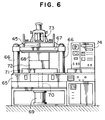
- Fig. 6 is a front view showing a transfer molding apparatus according to another embodiment of the present invention.
- Fig. 7 is a partially cutaway enlarged front view showing an essential portion of the apparatus shown in Fig. 6.
- the transfer molding apparatus includes plural posts 66 fixed on a pedestal 65.
- Each post 66 has a stationary platen 67 secured on the top end thereof.
- the stationary platen 67 is fixed with an upper unit 68.
- a numeral 71 denotes a movable platen fitted to a rod 70 of a cylinder 69 to be hydraulically operated.
- the movable platen 71 is fixed with a lower unit 72.
- a cylinder 73 for driving a plunger 45 is fitted to the stationary platen 67.
- These cylinders 69 and 73 are controlled by a control unit 74 fixed on the pedestal 65.
- Fig. 7 is a view showing the details of the upper unit 68 and the lower unit 72.
- the upper unit 68 has an upper base member 75 to which an upper die 76 served as a first die is fitted.
- the lower unit 72 has a lower base member to which a lower die 78 served as a second die is fitted.
- the lower die 78 is moved closer to or off the upper die 76 in synchronization with the vertical operation of the movable platen 71 caused by the cylinder 69.
- the matching of both dies 76 and 78 results in forming a cavity 43 for a package 43a made of resin on a die matching face called as a parting face or a mold separating face.
- Each of the base members 75 and 77 has a heater 79 built therein, which operates to heat the corresponding die 76 or 78.
- a numeral 44 denotes a cylindrical pot 44 passing through the upper base member 75. The pot 44 is fitted to the upper die 76. The plunger 45 is fitted inside of the pot 44 so that the plunger 45 may freely slide on the axis of the pot 44. This plunger 45 is driven by the cylinder 73 as shown in Fig. 6. In the pot 44, there is located a tablet 46 made of resin. This tablet 46 is pressed and shifted into the cavity 43 formed on the matching face of the dies 76 and 78.
- a runner 47 for communicating the pot 44 with the cavity 43 is formed on the matching face.
- the inlet of the runner 47 to the cavity 43 is a gate 48.
- Fig. 8 is a plane view showing the lower die 78.
- eight chase blocks 80 and a center block 81 compose the lower die 78.
- Each chase block has cavities 43 formed for a package 43a.
- the center block 81 has a runner 47 formed to communicate with each cavity 43.
- the lower die 78 has a cull space 82 in which cull, that is, resin overflown out of the runner 47, is left.
- the cull space 82 matches to the pot 44 fitted to the upper die 76.
- the lower die 78 is structured to have eight chase blocks. Any number of chase blocks, for example, four or six chase blocks may be selected if necessary.
- the structure employs a single pot type having a single pot. Two or more pots may be provided.
- Fig. 9 is an enlarged section partially showing the upper and the lower dies 76 and 78.
- the upper die 78 includes a protecting block 83 fitted to the upper base member 75 and a cavity block, that is, a die body 84 for forming the cavity 43 for molding the package 43a, the die body 84 located in the block 83.
- the die body 84 is formed of a porous material. As shown in Fig. 10, the die body 84 has a porous structure having air vents 85.
- the lower die 78 includes a protecting block 86 fitted to the lower base member 77 and a die body 87 for forming a cavity for molding the package 43a, that is, a cavity block, located in the block 86.
- the die body 87 is formed of a porous material. So, the die body 87 employs a porous structure having air vents.
- each of the filter layers 88 and 89 includes communicating pores 90. Those communicating pores 90 allow only the gas in the space such as the cavity 43 formed between the die bodies to pass through the air vents formed in the die bodies 84 and 87 and disallow the molten resin to pass through the air vents 85. That is, those communicating pores 90 serve to separately discharge the gas out of the die bodies. It means that each of the filter layers 88 and 89 is a kind of membrane.
- Fig. 10 is a partially enlarged section showing the die body 84 of the upper die 76 and the filter layer 88 formed on the surface of the die body 84.
- the die body 84 is formed of a porous material and has air vents 85, each average opening size of which is D.
- Each of the communicating pores 90 formed in the filter layer 88, which serves to separately discharge the gas, has an opening size of d.
- the opening size D of each air vent 85 and the opening size d of each pore 90 formed in the filter layer 88 are set so that the relation of D > Sr > d > Sg is established.
- Each of the die bodies 84 and 87 includes an exhaust space 93 or 94 facing the protecting block 83 or 86.
- Each of the exhaust spaces 93 and 94 communicated with the outside through an exhaust path 93a or 94a.
- a vacuum pump may be connected to each of the exhaust pipes 93a and 94a for sucking the air.
- the die body 84 or 87 has an exhaust concave portion 95 located outside of the die 76 or 78.
- the filter layers 88 and 89 are also formed.
- the exhaust concave portion 95 communicates with the outside through an exhaust through ditch 95a formed in the lower die 78.
- the gas left in the cavity 43 passes through the filter layers 88 and 89 and then through the air vents 85 formed in the porous material. Then, the gas is flown in the exhaust concave portion 95, and then is exhausted from the exhaust through ditch 95a to the outside.
- the exhaust concave portion 95 may be excluded.
- the exhaust through ditch 95a may be formed in the upper die 76 or both of the upper and the lower dies 76 and 78.
- the die bodies 84 and 87 are formed to have air vents 85 by using sintered metal.
- a more fluidizing material than the mold resin is implanted to the opening for burying a part of an opening of the air vent 85.
- the same resin as the mold material may be used for molding the product at a higher pressure than a normal mold pressure, for blocking part of an opening of the air vent 85 having a larger size than a constant one and making the diameter of the air vent smaller.
- a porous micro filter area made of a thin film is formed to have lots of communicating pores 90 each having a smaller diameter than the inner diameter of the air vent 85 of the die body, that is, the ground material.
- the micro filter area provides the filter layers 88 and 89 with the function of separating the air left in the die when molding a product or gas generated in the die when molding the product from the resin material. That is, the filter layers are served as separating films.
- a semiconductor chip 41 is mounted on a lead frame 42 in advance.
- the lead frame 42 has plural inner leads electrically connected with an electrode formed on the first main face of the semiconductor chip 41 with a wire.
- the resulting lead frame becomes a chip-lead compound 40.
- the chip-lead compound 40 is located between the dies 76 and 78. Then, the movable platen 71 is lifted up by the cylinder 69 for moving the lower die 78 closer to the upper die 76. This movement allows the spaces containing the mold cavities to be formed on the surfaces of the dies. The chip-lead compound 40 is fixed in the spaces. Then, the solid tablet 46 whose viscosity is made lower by a pre-heater is put into the pot 44, and the tablet 46 molten by the heater 79 is pressed by the plunger 45. As a result, the resin material is flown in the cavity 43 through the runner 47 and the gate 48.
- the molten mold resin pressed and shifted in the cavity 43 is flowing in the cavity 43 as the gas such as air left in the cavity 43 is flowing in the air vents 85 formed in the die bodies 84 and 87 through the communicating pores 90 formed in the filter layers 88 and 89.
- Fig. 9 shows the state in which on the border of the chip-lead compound 40, the resin on the side of the lower die 78 flows faster, hits the end of the cavity 43 in the downstream of the gate 48, passes the gap of the chip-lead compound 40 and flows up to the upper die 76.
- Gas such as air is left in the empty portion 96 where no molten resin in the upper die 76 is not still flown.
- the gas passes through the communicating pore 90 (see Fig. 10) formed in the filter layer 88 around the empty portion 96 and then is discharged out of the upper die 76 through the exhaust space 93 and the exhaust pipe 93a as shown in Fig. 9.
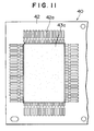
- the resin is pressed and filled in the cavity 43 in which the resin is heated and hardened. Then, in response to a control signal sent from a control unit 74 shown in Fig. 6, the movable platen 71 is lifted down so that the upper die 76 is separated from the lower die 78. After both dies are off, as shown in Fig. 11, the chip-lead compound 40 is released in which the package 43a is formed of the resin. This release is done by the ejector pins. In place, by supplying compressed air from the exhaust pipes 93a and 94a for injecting air from the communicating pores 90, it is possible to remove the molded chip-lead compound 40.
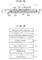
- the chip-lead compound 40 having the package 43a formed therein is made to be a semiconductor integrated circuit device shown in Fig. 12.
- a numeral 97 denotes a tab, on which a semiconductor chip 41 is pasted through an adhesive material 98 such as sliver paste.
- the semiconductor chip 41 has the electrode pad 41a and the inner lead 42b, both of which are electrically connected through a conductive wire 99 made of gold (Au) or aluminium (Al). The electric connection makes it possible to apply a supply voltage and do the I/O of a signal from the outside to the semiconductor chip 41 through the outer lead 42a.
- the semiconductor integrated circuit device shown in Fig. 12 has a width A of about 10 mm and a thickness B of about 1 mm. Inside of the IC device is sealed the semiconductor chip 41 whose thickness size C is about 0.4 mm. This is a resin-sealed type. Even such a thin type may be manufactured at a high yield without physically transforming it.
- Fig. 13 shows a process for manufacturing the foregoing semiconductor integrated circuit device.
- the semiconductor chip 41 is fitted on the tab 97 of the lead frame 42.
- the electrode pad 41a and the inner lead 42b of the semiconductor chip 41 are electrically connected through the wire 99.
- the process 1 for forming the chip-lead compound 40 is terminated, in which process the chip-lead compound 40 is prepared.
- This chip-lead compound 40 is transferred to the transfer molding apparatus. Then, in the process 2, the compound 40 is placed on the die of the molding apparatus. Next, in the process 3, the dies are matched for mold clamping. After the mold clamping, in the process 4, the tablet 46 is inserted to the pot 44. After the insertion, the plunger 45 starts to press the tablet 46. Then, in the process 5, the resin is implanted. After the implantation, the dies are kept in the mold clamping for a several minutes and then the resin is hardened. In addition, the insertion of the tablet in the process 4 may be executed in advance of the placement of the chip-lead compound 40 on the die.
- the separating process 6 is executed and then the chip-lead compound 40 is released from the dies in which compound the package 43a is formed.
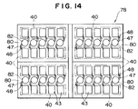
- Fig. 14 shows the lower die 78 provided in the transfer molding apparatus according to another embodiment of the present invention, in which the shown portion corresponds to that shown in Fig. 8.
- the components common to those shown in Fig. 8 have the same reference numbers.
- This transfer molding apparatus has plural pots.
- the lower die 78 provides four chase blocks 80, each of which has five cull spaces 82 corresponding to the pots. Each cull space 82 is connected to the concave portions of the two cavities 43 through the runner 47 and the gate 48. Any number of blocks may compose the lower die 78. Each block 80 may any number of cavities 43 formed therein.
- the chip-lead compound 40 placed on the lower die 78 is shown in a two-dot chain line.
- the process 4 of inserting the tablet 46 shown in Fig. 13 into the pot 44 is executed before the process 2 of placing the chip-lead compound 40 on the die.
- the other processes are likewise to the foregoing manufacturing process.
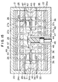
- Fig. 15 shows a transformation of the transfer molding apparatus shown in Figs. 3 and 4.
- the components common to those shown in Figs. 3 and 4 have the same reference numbers.
- the corresponding portions of the upper die body 24 and the lower die body 34 to the insides of the cavities 43 and the runners 47 formed for clamping the upper and the lower dies are made of a porous material.
- the die bodies 24 and 34 each include cavity blocks 24a and 34a for forming one cavity 43, and each of the cavity blocks 24a and 34a is formed of a porous material for making a ventilating portion.
- the corresponding portions of the die bodies 24 and 34 to the runner 47 are made of steel for the dies.
- Fig. 16 shows a transformation of the transfer molding apparatus shown in Fig. 15.
- Each of the cavity blocks 24a and 34a is formed of steel for the die. Hence, those blocks are not ventilative, while the portions corresponding to the runner 47 are formed of a porous material and thus are ventilative.
- the pot 44 and the plunger 45 are also formed of a porous material. Hence, when the plunger 45 is pressing the resin tablet 46 so that the resin tablet 46 is filled in the cavity 43 through the runner 47, before the resin reaches the cavity 43, the air or gas left in the pot 44 and the runner 47 are discharged out of the exhaust port 49 through the ventilative pot 44, die bodies 24 and 34 and through the ventilative plunger 45.
- air vents are provided in the cavity so that air left in the cavity is discharged through the air vents.
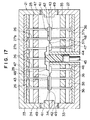
- Fig. 17 shows a transformation of the transfer molding apparatus shown in Fig. 16.
- the die bodies 24 and 34 for forming the cavity 43 and the runner 47, the pot 44, and the plunger 45 are all formed of a porous material.
- the plunger 45 shown in Figs. 16 and 17 may have only its tip portion formed of the porous material so that the tip portion may be made ventilative.
- Fig. 18 shows the transfer molding apparatus according to another embodiment of the present invention, in which the portion of the apparatus corresponding to that shown in Fig. 9 is shown.
- the components common to those shown in Fig. 9 have the same reference numbers.
- the gate 48 is formed in the die body 87 of the lower die 78.
- the resin implanted from the gate 48 to the cavity 43 is located as opposed to the gate 48 and finally filled in the portion corresponding to the upper portion of the cavity 43.
- a ventilating portion 84a made of a porous material is formed in a manner to correspond to the portion where the resin is finally filled.
- the filter layer 88 is formed on the surface of the ventilating portion 84a.
- This transfer molding apparatus may take the illustrative structure by partially improving the conventional die.
- the gate 48 is formed by forming the concave portion in the die body 84 of the upper die, the portion to which the resin is finally filled is located as opposed to the gate 48 and is made to be the portion corresponding to the lower portion of the cavity 43.
- the ventilating portion 84a in the die body 87 of the lower die 78 in a manner to correspond to the corresponding portion or form the ventilating portions 84a in each die body of the upper and the lower dies.
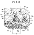
- Fig. 19 shows the die body 84 of the upper die 76 provided in the transfer molding apparatus according to another embodiment of the present invention, in particular, the portion of the die body corresponding to that shown in Fig. 10.
- the die body 84 is formed of a porous material such as sintered metal having metallic or ceramic powder.
- the die body 84 has air vents 85 and thus is structured to be porous.
- a fine porous portion 100 formed of fine particles 101 coupled by a bonding agent is buried to a predetermined depth from the surface of the die body 84.
- the fine particles 101 are metallic or ceramic, and the bonding agent 102 may be a wax material to be molten at about 200 to 500°C, for example.
- the fine porous portion 100 includes communicating pores 90 that communicate with the air vents 85 and have smaller diameters than the air vents 85. This serves to inhibit intrusion of the resin into the die body 84 and allows at least part of gas components to pass through the communicating pores 90 for preventing occurrence of voids in the package 43a.
- the air vent 85 has an average inner diameter of about 3 ⁇ m or more. Of many communicating pores 85, some may have a larger inner diameter of an opening, for example, about several tens ⁇ m or more. If so, since the fine porous portion 100 is buried into each opening of the air vent and extended to a predetermined depth, the fine openings of the communicating pores 90 are formed on the surface of the die body 84.
- the average inner diameter of the communicating pore 90 is about 2.5 ⁇ m or less, or about 0.5 ⁇ m or less. The average diameter is selected according to the kind of resin to be used for the mold.
- the fine porous portion 100 By burying the fine porous portion 100 to a predetermined depth of the air vent 85, it is possible to shorten the gas-passing area of the fine communicating pore 90. Since the air vent 85 has a larger inner diameter than the communicating pore 90, it is possible to keep the ventilation resistance of gas flowing through the die body 84 lower.
- the die body 84 of the upper die 76 is shown in Fig. 19.
- the die body 87 of the lower die 78 is formed in the same manner.
- the process is executed to compose the die bodies 84 and 87 from sintered metal so that those die bodies have the air vents 85.
- the fine particles 101 made of a proper material to a die material are coupled with one another, and a wax material served as a coupling material 102 is mixed with the fine particles 101 for coupling the fine particles 101 on the inner surface of each communicating pore 85.
- the mixture is coated on the surface of the die body.
- the predetermined process such as heating is executed to couple the fine particles 101 with one another and couple the fine particle 101 with the inner surface of the air vent 85.
- the fine porous portion 100 is formed inside of the air vent 85. In place, on the surface of the die body 84 or 87, the fine porous portion 100 may be formed.
- the fine porous portion 100 may be a mixture of the fine particles 101 with the grain wax material served as the coupling material 102. Or, it may be possible to apply a coat of the wave material on the surface of the fine particles 101.
- the coupling material 102 it is possible to use a heat-resistant adhesive agent such as an epoxy or polyimide system in place of the wax material.
- a heat-resistant adhesive agent such as an epoxy or polyimide system in place of the wax material.
- the adhesive agent is coated on the surfaces of the fine particles 101, and then the coated fine particles 101 or the mixture of the adhesive agent with the fine particles is buried in the air vents 85.
- the fine porous portion 100 may be formed of only the fine particles 101.
- the fine particles 101 are heated up to around a melting point for melting and coupling the fine particles 101 with one another and the fine particles 101 with the inner surfaces of the air vents 85. The melting and coupling results in forming the fine porous portion 100.
- the fine porous portion 100 without the coupling material 102 it is possible to use the fine particles 101 having a larger thermal expansion coefficient than a mother material of the die body 84 or 87. In this case, after the fine particles 101 are filled in the air vents 85 at a low temperature, then, the temperature of those particles is returned to a normal temperature, so that the fine particles 101 are coupled through the effect of the thermal stress caused by the difference between the thermal expansion coefficients, for composing the fine porous portion 100.
- This type of fine porous portion 100 are expanded by the heat of the mold resin, and when the dies are in use, the coupling force of the fine particles 101 is made stronger.
- the fine porous portion 100 As another method for forming the fine porous portion 100, it is possible to use a mixture of a grain vaporizing material that is to be sublimed or vaporized at a predetermined temperature with a burying material, that is, the fine porous portion 100 formed by solidifying or hardening the grain vaporizing material at a lower temperature or at the substantially same temperature. In this case, after this mixture is filled in the air vents 85, the mixture is heated up to the subliming or vaporizing temperature. At that time, when or before the grain vaporizing material is vaporized, the burying material is hardened. The resulting fine porous portion 100 is formed of the burying material and has voids corresponding to the volumes of the vaporizing material.
- the vaporizing particles In place of the vaporizing particles, it is possible to use a mixture of a foaming material with a coupling material for forming the fine porous portion 100.
- a foaming material When heating the foaming material, fine foams are generated from the foaming material.
- the mixture is heated for generating many foams.
- the resulting fine porous portion 100 is formed of only the fine grain coupling material and has the communicating pores corresponding to the foams generated in the foaming material.
- the fine porous portion 100 a highly elastic material such as rubber may be used for the coupling material 102.
- the fine porous portion 100 is transformed by the pressure applied by the resin when molding the package. That is, the pressure serves to shrink the communicating pores 90. This automatically prevents intrusion of more than a constant amount of mold resin into the air vents 85.
- the state of the communicating pores 90 are returned to the original one by the force of elasticity, that is, the communicating pores 90 are made larger. This serves to reduce the ventilation resistance against the gas when the gas is supplied from the outside for separating the chip-lead compound 40 from the dies.
- Fig. 20 shows a transformation of the transfer molding apparatus, in particular, the portion of the apparatus corresponding to that shown in Fig. 19.
- a coating layer 103 is formed on the surface of the die body 84.
- This coating layer 103 is formed on the surface of the die body 84 as shown in Fig. 19 by means of the plating or vacuum vaporizing means.
- For the coating it is possible to use various kinds of surface coating methods such as Cr or Tin Plating.
- Cr or Tin Plating By controlling the coat thickness and the coating method, it is possible to set the size d of the opening of the communicating pore 90 to the most approximate value.
- the coating layer 103 as described above, it is possible to stubbornly fix the fine porous portion 100 inside of the air vent 85.
- the coating layer 103 is formed, it is possible to form the fine porous portion 100 of only the fine particles 101 without using the coupling agent 102 such as a wax material served as the fine porous portion 100. Further, without melting and coupling the fine particles 101 with one another, it is possible to prevent the fall of the particles of fine porous portion 100 from the air vent 85.
- the filter layer 88 shown in Fig. 10 may be formed on the surface of the porous material included in the transfer molding apparatus as shown in Figs. 3 to 5 or 15 to 17. Or, as shown in Figs. 19 to 20, the fine porous portion 100 may be formed on the surface.
- the illustrative lead frame 42 provides the tab 97.
- another kind of lead frame may be formed to have no lead frame.
- the semiconductor chip 41 is laminated on the inner lead 42b so that the second face, that is, the face having no circuit of the semiconductor chip 41 is opposed to the inner lead 42b.
- the electrode pad 41a formed on the first face is electrically connected to the inner lead 42b through a wire 99.
- the resulting compound is made to be a COL (Chip On Lead) type semiconductor integrated circuit device.
- the semiconductor chip 41 is laminated on the inner lead 42b so that the first face, that is, the face having a circuit formed thereon of the semiconductor chip 41 is opposed to the inner lead 42b.
- the inner lead 42b is directly connected to the electrode formed on the semiconductor chip 41 through a solder electrode.
- the resulting compound is made to be an LOC (Lead On Chip) type semiconductor integrated circuit device.
- the illustrative chip-lead compound 40 provides the lead frame 42.
- the chip-lead compound may use a thin film wiring sheet.
- the illustrative transfer molding apparatus is constructed so that the lower die may move to or off the upper die by vertically moving the lower die. In place, the lower die may be fixed and the upper die may be vertically moved. Moreover, both of the dies are allowed to be horizontally moved to or off each other.
- the inventions designed mainly by the present inventors have been applied to the manufacture of a QFP type semiconductor integrated circuit device.
- the present invention is not limited to it.
- the invention may apply to the manufacture of a DIP (Dual In-Line Package) type semiconductor integrated circuit device, a PLCC (Plastic Leaded Chip Carrier) type or an SOJ (Small Outline J-Leaded Package) type semiconductor integrated circuit device, the latter two of which are sealed by the resin.
- Fig. 21 is a model view showing an essential portion of the transfer molding apparatus according to an embodiment of the present invention (embodiment 11).
- Fig. 22 is a perspective view showing an outer appearance of the transfer molding apparatus.
- Fig. 23 is a partially cutaway plane view showing a molding section of the transfer molding apparatus.
- Fig. 24 is a schematic section showing the opened dies.
- Fig. 25 is a schematic section showing the dies stays in the molding state.
- Fig. 26 is a schematic view showing the opened dies.
- the transfer molding apparatus as shown in Fig. 21, is constructed so that a material 105 to be molded is located between the parting face 123a of the upper die 123 and the parting face 124a of the lower die 124 of the die 120 for molding the resin.
- the material 105 to be molded is structured so that a semiconductor chip 108 is fixed on a supporting plate (tab) 107 of a lead frame 106 and an inner end of a lead 109 is connected to an electrode (not shown) of the semiconductor chip 108 through a conductive wire 104.
- the semiconductor chip 108, the wire 104 and the inner portion of the lead 109 are sealed by the resin.
- the material 105 to be molded is transferred from a loader 101 to a molding section (resin molding section) 102, in which the mold is executed. Then, the molded product is transferred out to the unloader 103 in which the molded product is held.
- a numeral 121 denotes an upper unit.
- a numeral 122 denotes a lower unit.
- the resin molding section 102 is constructed so that plural guide posts 111 are vertically fixed on a pedestal 110 and each of the guide posts 111 provides a stationary platen 112 fixed on the upper end.
- the guide post 111 provides a movable platen 113 to be vertically moved.
- the movable platen 113 provides a driving block 114 fixed on the lower end.
- the driving block 114 is supported by a rod 116 of a press jack 115 fixed on the pedestal 110 to be operated by oil or air pressure.
- the driving block 114 is lifted up and down in synchronization to the vertical movement of the rod 116.
- the operation of the press jack 115 allows the movable platen 113 to be lifted up and down.
- the upper unit 121 is fixed on the lower surface of the stationary platen 112.
- the lower unit 122 is fixed on the upper surface of the movable platen 113.
- the upper unit 121 is fitted to the upper die 123.
- the lower unit 122 is fitted to the lower die 124.
- the upper and the lower dies 123 and 124 are fixed on the protecting frames 125 and 126 of the upper and the lower units 121 and 122, respectively.
- the parting face 123a of the upper die 123 is opposed to the parting face 124a of the lower die 124.
- Those parting faces 123a and 124a provide resin press-fitting portions 130 and 131, respectively.
- the resin press-fitting portion is concave and includes the cull 130a, the runner 130b, the gate 130c and the cavity 130d.
- These upper and lower dies 123 and 124 do not provide an over-runners, dummy cavities, air vents, and flow cavities as well as ejector pins.
- the die 120 has a simple structure, so that the design of the die 120 may be easier and the manufacturing time of the die 120 may be made shorter.
- the driving block 114 provides a transfer jack 117 fitted thereon.
- the transfer jack 117 has a piston rod 118, which is entered into a pot 119 located in the lower unit 122 for pressing a resin tablet put in the pot 119.
- molten resin 128 is flown into the cavity 130d through the cull 130a, the runner 130b and the gate 130c.
- the upper die 123 is formed of a porous material through which gas such as air is allowed to pass, so the upper die 123 includes a ventilating portion 123b (base ventilating portion). So is the lower die 124. Hence, the lower die 124 includes a ventilating portion 124b (base ventilating portion).
- the porous material is formed by sintering metal powder or ceramic powder. These ventilating portions 123b and 124b include communicating pores whose diameter is 1 ⁇ m to several ⁇ m, through which air is allowed to freely pass.
- the flow path block 135 provides flow paths extending horizontally and communicated with each other. So is the flow path block 136.
- the communicating pores 139 and 140 communicate with the flow paths 137 and 138. Hence, gas is allowed to pass through the ventilating portions 123b and 124b and the flow paths 137 and 138.
- Each of the flow paths 137 and 138 is connected to plural communicating pipes 141.
- Each communicating pipe 141 is connected to a vacuum pump 145 served as sucking means or a compressor 146 served as means for supplying compressed gas.
- the communicating pipe 141 is branched into branch pipes, each tip of which is connected to the vacuum pump 145 or the compressor 146.
- the communicating pipe 141 provides a valve 147 at a predetermined spot, which valve is to be automatically shut or opened.
- Fig. 21 is a conceptual section showing the embodiment 11, in which the flow path blocks 135 and 136 are removed and each component is simplified.
- the porous films 150 and 151 have ventilating portions (surface ventilating portion) 150a and 151a through which air is allowed to pass.
- Each air vent of the ventilating portions 150a and 151a has a larger diameter than that of the ventilating portions 123b and 124b of the upper and the lower dies 123 and 124.
- the former air vent has a diameter of about 0.1 to 1 ⁇ m.
- This embodiment 11 selects a diameter of 0.5 ⁇ m.
- the minimum grain diameter of the molten resin for molding a semiconductor device is about 1 ⁇ m.
- porous films 150 and 151 heat-resistant films are selected so that those films are allowed to resist the heat appearing in molding the semiconductor device.
- it may use tetrafloroethylene resin film that covers the temperature range from - 120 to 260°C.
- the porous films 150 and 151 are as thin as 300 ⁇ m or less, because these films have to be transformable.
- the porous film 151 extending on the lower die 124 has a pore corresponding to the pot 119. As such, the molten resin in the pot 119 is flown into the cull 130a, the runner 130b and the gate 130c and then is filled in the cavity 130d.
- the porous films 150 and 151 are formed like a long tape and has the substantially same width as the upper and the lower dies 123 and 124. Those films extend on the overall areas of the parting faces 123a and 124a of the upper and the lower dies 123 and 124.
- the porous films 150 and 151 as shown in Figs. 23 and 24, are sequentially fed between the parting faces 123a and 124a through the effect of the porous film feeding mechanisms 152 and 153.
- the porous film feeding mechanisms 152 and 153 are constructed to have feed rolls 152a and 153a around which the films 150 and 151 are wound, take-up rolls 152b and 153b around which the films being fed are wound, and a driving section (not shown) for rotating the feed rolls 152a and 152b, respectively.
- the feed roll 152a or 153a and the take-up roll 152b or 153b are located on both side of the upper die 123 or the lower die 124.
- the porous films 150 and 151 being fed from the feed rolls 152a and 153a extend between the parting face 123a of the upper die 123 and the parting face 124a of the lower die 124 and then are taken up around the take-up rolls 152b and 153b, respectively.
- the ventilating portions 123b, 124b and 150a, 151a compose a two-stage ventilating portion.
- the valve 147 is controlled so that the upper and the lower dies 123 and 124 are entered into the sucking discharge state, the vacuum pump 145 are operated, and the porous films 150 and 151 are made in close contact with the surfaces of the resin press-fitting portions 130 and 131. Then, the semiconductor chip 108 is fixed on the lead frame 106. Next, the material 105 to be molded in which the electrode and the wire of the semiconductor chip 108 are electrically connected with the wire is transferred onto the parting face 124a of the lower die 124. Fig. 24 shows the material 105 to be molded is floated. In actual, the material 105 is placed on the porous film 151. The porous films 150 and 151 remain before transformation.
- the lower unit 122 is lifted up for mold clamping. Then, the transfer jack 117 is operated so that the piston rod 18 serves to press the resin tablet. The press makes the resin tablet molten. The molten tablet is flowing through the cull 130a, the runner 130b, and the gate 130c into the cavity 130.
- the air left in the resin press-fitting portions 130 and 131 are sucked by the vacuum pump 145.
- the sucked air is put into the ventilating portions 150a and 151a of the porous films 150 and 151 and the ventilating portions 123b and 124b of the upper and the lower dies 123 and 124 and then enters into the communicating pores 139 and 140.
- the air is discharged out of the die 120 through the communicating pipe 141.
- the air left in the resin press-fitting portions 130 and 131 such as the cavity 130b are smoothly discharged out by the vacuum pump without bringing about any disturbance.
- the air is not entrained in the resin 128 filled in the cavity 130b. It means that no void is generated in the mold (package) 159.
- the implanting press of the resin 128 serves to make the porous films 150 and 151 be in close contact with the wall surface of the cavity 130d.
- the resulting mold is made to be a complete one with no impairment of its outer appearance.
- the vacuum pump 145 is stopped.
- the valve 147 is automatically switched by a proper means (not shown) so that the ventilating portion is made to be in the state of supplying the compressed gas.
- the dies are opened.
- the compressor 146 is operated so that the compressed air is fed into the resin press-fitting portions 130 and 131.
- the pressure of the compressed air and the restoring force of the porous films 150 and 151 caused by the drawing of the take-up rolls 152b and 153b serve to push the mold 160 out of the resin press-fitting portions 130 and 131.
- This push-out is made possible only by the compressed air or the restoring force of the films 150 and 151.
- both of the compressed air and the restoring force that is, the levelling force make the push-out more secure.
- the porous film feeding mechanisms 152 and 153 starts to rotate the rolls so that a new portion of each film is located between the parting face 123a of the upper die 123 and the parting face 124a of the lower die 124. This way of use makes it possible to implement the molding process without any clogging.
- the transfer molding method and apparatus according to the embodiment 11 provide the following effects.
- Fig. 27 is a schematic section showing dies provided in another embodiment (embodiment 12) of the present invention.
- the upper and the lower dies 123 and 124 provide the resin press-fitting portions 130 and 131 on which the porous films 165 and 166 are pasted, respectively.
- these porous films 165 and 166 are replaced with new ones.
- this embodiment offers the same effect as the embodiment 11.
- Fig. 28 is a schematic section showing dies provided in another embodiment (embodiment 13) of the present invention.
- the upper and the lower dies 123 and 124 provide the resin press-fitting portions 130 and 131 on which porous films 170 and 171 are formed.
- These porous films 170 and 171 are formed of a coat of titanium nitride (TiN), chromium (Cr) or the like.
- the coat has a thickness of about 1 ⁇ m to 5 ⁇ m and is applied by an electrolytic process.
- the coat is porous and thus contains lots of air vents, each of whose diameter is about 0.1 ⁇ m to 0.3 ⁇ m.
- This kind of structure is resistant against clogging because it is a coating film and contains air vents through which resin particles are not permitted to pass. Hence, the structure is durable for a long time.
- Fig. 29 is a model view showing an essential portion of the transfer molding apparatus according to another embodiment (embodiment 24) of the present invention.
- the upper and the lower dies 123 and 124 are formed of not a porous material but a normal hard metal.
- the base ventilating portions 123b and 124b are formed of pores made on the upper and the lower dies 123 and 124. Those pores are connected to the communicating pipe 141. If these ventilating portions 123b and 124b are located at least in the cavity 130d, no void takes place in the resulting mold.
- the base ventilating portions 123b and 124b formed of pores may apply to the foregoing embodiments 11 and 12.
- the foregoing description has been concerned with the transfer molding technique that corresponds to the background of the present invention.
- the applied field of the present invention is not limited to it.
- the invention may apply to a normal injection molding press for molding only a resin from only resin or a technique for molding a molten material such as die cast or rubber molding.
- the present invention may apply to at least the molding technique.
Landscapes
- Engineering & Computer Science (AREA)
- Manufacturing & Machinery (AREA)
- Mechanical Engineering (AREA)
- Encapsulation Of And Coatings For Semiconductor Or Solid State Devices (AREA)
- Moulds For Moulding Plastics Or The Like (AREA)
Applications Claiming Priority (8)
| Application Number | Priority Date | Filing Date | Title |
|---|---|---|---|
| JP283278/94 | 1994-11-17 | ||
| JP283277/94 | 1994-11-17 | ||
| JP28327894 | 1994-11-17 | ||
| JP28327794 | 1994-11-17 | ||
| JP101833/95 | 1995-04-26 | ||
| JP10183395A JPH08294919A (ja) | 1995-04-26 | 1995-04-26 | モールド方法およびモールド装置 |
| JP224245/95 | 1995-08-31 | ||
| JP22424595A JPH08192438A (ja) | 1994-11-17 | 1995-08-31 | 半導体集積回路装置の製造方法およびそれに用いるモールド装置 |
Publications (2)
| Publication Number | Publication Date |
|---|---|
| EP0713248A2 true EP0713248A2 (fr) | 1996-05-22 |
| EP0713248A3 EP0713248A3 (fr) | 1997-04-23 |
Family
ID=27468957
Family Applications (1)
| Application Number | Title | Priority Date | Filing Date |
|---|---|---|---|
| EP95307982A Withdrawn EP0713248A3 (fr) | 1994-11-17 | 1995-11-08 | Procédé de moulage et appareil |
Country Status (3)
| Country | Link |
|---|---|
| EP (1) | EP0713248A3 (fr) |
| KR (1) | KR100392264B1 (fr) |
| TW (1) | TW302527B (fr) |
Cited By (17)
| Publication number | Priority date | Publication date | Assignee | Title |
|---|---|---|---|---|
| EP0795901A3 (fr) * | 1996-03-14 | 1999-10-27 | Towa Corporation | Procédé de scellement d'un composant électronique par une résine moulée |
| EP0979718A1 (fr) * | 1998-08-06 | 2000-02-16 | Franz Sterner | Procédé de fabrication d'articles moulés par injection et moule d'injection pour la mise en oeuvre du procédé |
| EP0933808A3 (fr) * | 1998-01-23 | 2000-03-22 | Apic Yamada Corporation | Procédé et appareillage pour l'encapsulation par résine d'un dispositif semiconducteur |
| NL1011392C2 (nl) * | 1999-02-25 | 2000-08-28 | 3P Licensing Bv | Inrichting voor het omhullen van elektronische componenten en daarvoor bestemde matrijs. |
| WO2006011878A1 (fr) * | 2004-06-28 | 2006-02-02 | Ex One Corporation | Moules permeables aux gaz |
| EP0935817A4 (fr) * | 1996-07-25 | 2006-08-02 | Advanced Systems Automation | Moule de grille matricielle a billes pour l'encapsulation sur des substrats d'epaisseurs variables |
| DE102005020427A1 (de) * | 2005-04-29 | 2006-11-09 | Infineon Technologies Ag | Verfahren und Gießformwerkzeug zur Herstellung einer Schutzschicht an integrierten Bauelementen |
| US7287975B2 (en) | 2003-06-12 | 2007-10-30 | Towa Corporation | Resin mold material and resin mold |
| US7732037B2 (en) * | 2004-02-09 | 2010-06-08 | Towa Corporation | Conductive porous material, resin molding die employing the same, and method of preparing conductive porous material |
| US7784764B2 (en) * | 2004-11-02 | 2010-08-31 | Towa Corporation | Low-adhesion material, mold for molding resin using the same and contaminant adhesion preventing material |
| US20120076886A1 (en) * | 2004-03-26 | 2012-03-29 | Takaki Kuno | Method of evaluating adhesion property, low-adhesion material, and mold for molding resin |
| CN110978435A (zh) * | 2019-12-19 | 2020-04-10 | 惠州市吉邦精密技术有限公司 | 一种自动射蜡模具设备 |
| WO2021121659A1 (fr) * | 2019-12-20 | 2021-06-24 | Eaton Intelligent Power Limited | Moule d'encapsulation à paroi perméable |
| CN113165235A (zh) * | 2018-11-30 | 2021-07-23 | 美国斯耐普公司 | 低压模塑制品及其制造方法 |
| CN116001201A (zh) * | 2022-12-05 | 2023-04-25 | 大能(南通)机电有限公司 | 一种可调节温度的机电一体化模具及其使用方法 |
| CN116666229A (zh) * | 2023-08-02 | 2023-08-29 | 西安畅榜电子科技有限公司 | 一种芯片框及其加工方法 |
| EP3620253B1 (fr) * | 2018-08-22 | 2024-10-09 | General Electric Company | Outils poreux et leurs procédés de fabrication |
Family Cites Families (9)
| Publication number | Priority date | Publication date | Assignee | Title |
|---|---|---|---|---|
| DE1779104A1 (de) * | 1968-07-06 | 1971-08-19 | Continental Gummi Werke Ag | Verfahren und Vorrichtung zum Herstellen von Gummi- oder Kunststoffartikeln |
| JPS6237119A (ja) * | 1985-08-10 | 1987-02-18 | Fujitsu Ltd | モ−ルド金型およびモ−ルド方法 |
| JPS62135330A (ja) * | 1985-12-09 | 1987-06-18 | Rohm Co Ltd | トランスフア−成形方法 |
| JPS62173228A (ja) * | 1986-01-27 | 1987-07-30 | Rohm Co Ltd | トランスフア−成形方法 |
| JPH04129713A (ja) * | 1990-09-20 | 1992-04-30 | Matsushita Electric Works Ltd | 真空成形用金型装置 |
| JPH04307213A (ja) * | 1991-04-05 | 1992-10-29 | Seiko Epson Corp | トランスファーモールド型及びトランスファーモールド装置 |
| JPH0574827A (ja) * | 1991-09-13 | 1993-03-26 | Fujitsu Miyagi Electron:Kk | 半導体装置の製造装置 |
| JPH06344389A (ja) * | 1993-06-03 | 1994-12-20 | Fujitsu Miyagi Electron:Kk | モールド金型 |
| NL9400119A (nl) * | 1994-01-27 | 1995-09-01 | 3P Licensing Bv | Werkwijze voor het met een hardende kunststof omhullen van een electronische component, electronische componenten met kunststofomhulling verkregen door middel van deze werkwijze en matrijs voor het uitvoeren der werkwijze. |
-
1995
- 1995-09-26 TW TW084110042A patent/TW302527B/zh not_active IP Right Cessation
- 1995-11-08 EP EP95307982A patent/EP0713248A3/fr not_active Withdrawn
- 1995-11-16 KR KR1019950041623A patent/KR100392264B1/ko not_active Expired - Fee Related
Cited By (26)
| Publication number | Priority date | Publication date | Assignee | Title |
|---|---|---|---|---|
| EP0795901A3 (fr) * | 1996-03-14 | 1999-10-27 | Towa Corporation | Procédé de scellement d'un composant électronique par une résine moulée |
| EP0935817A4 (fr) * | 1996-07-25 | 2006-08-02 | Advanced Systems Automation | Moule de grille matricielle a billes pour l'encapsulation sur des substrats d'epaisseurs variables |
| EP0933808A3 (fr) * | 1998-01-23 | 2000-03-22 | Apic Yamada Corporation | Procédé et appareillage pour l'encapsulation par résine d'un dispositif semiconducteur |
| US6459159B1 (en) | 1998-01-23 | 2002-10-01 | Apic Yamada Corporation | Apparatus for sealing a semiconductor device utilizing a release film |
| SG96180A1 (en) * | 1998-01-23 | 2003-05-23 | Apic Yamada Corp | Resin sealing method and apparatus for a semiconductor device |
| EP0979718A1 (fr) * | 1998-08-06 | 2000-02-16 | Franz Sterner | Procédé de fabrication d'articles moulés par injection et moule d'injection pour la mise en oeuvre du procédé |
| NL1011392C2 (nl) * | 1999-02-25 | 2000-08-28 | 3P Licensing Bv | Inrichting voor het omhullen van elektronische componenten en daarvoor bestemde matrijs. |
| US7287975B2 (en) | 2003-06-12 | 2007-10-30 | Towa Corporation | Resin mold material and resin mold |
| US7732037B2 (en) * | 2004-02-09 | 2010-06-08 | Towa Corporation | Conductive porous material, resin molding die employing the same, and method of preparing conductive porous material |
| US20120076886A1 (en) * | 2004-03-26 | 2012-03-29 | Takaki Kuno | Method of evaluating adhesion property, low-adhesion material, and mold for molding resin |
| WO2006011878A1 (fr) * | 2004-06-28 | 2006-02-02 | Ex One Corporation | Moules permeables aux gaz |
| US7784764B2 (en) * | 2004-11-02 | 2010-08-31 | Towa Corporation | Low-adhesion material, mold for molding resin using the same and contaminant adhesion preventing material |
| DE102005020427A1 (de) * | 2005-04-29 | 2006-11-09 | Infineon Technologies Ag | Verfahren und Gießformwerkzeug zur Herstellung einer Schutzschicht an integrierten Bauelementen |
| EP4446045A3 (fr) * | 2018-08-22 | 2025-06-04 | General Electric Company | Outils poreux et leurs procédés de fabrication |
| EP3620253B1 (fr) * | 2018-08-22 | 2024-10-09 | General Electric Company | Outils poreux et leurs procédés de fabrication |
| US11927760B2 (en) | 2018-11-30 | 2024-03-12 | Snap Inc. | Low pressure molded article and method for making same |
| US12422685B2 (en) | 2018-11-30 | 2025-09-23 | Snap Inc. | Low pressure molded article and method for making same |
| CN113165235A (zh) * | 2018-11-30 | 2021-07-23 | 美国斯耐普公司 | 低压模塑制品及其制造方法 |
| CN110978435A (zh) * | 2019-12-19 | 2020-04-10 | 惠州市吉邦精密技术有限公司 | 一种自动射蜡模具设备 |
| US20220212374A1 (en) * | 2019-12-20 | 2022-07-07 | Eaton Intelligent Power Limited | Permeable Wall Encapsulation Mold |
| US11673298B2 (en) * | 2019-12-20 | 2023-06-13 | Eaton Intelligent Power Limited | Casting method for encapsulating an electrical component |
| US11318642B2 (en) | 2019-12-20 | 2022-05-03 | Eaton Intelligent Power Limited | Permeable wall encapsulation mold |
| WO2021121659A1 (fr) * | 2019-12-20 | 2021-06-24 | Eaton Intelligent Power Limited | Moule d'encapsulation à paroi perméable |
| CN116001201A (zh) * | 2022-12-05 | 2023-04-25 | 大能(南通)机电有限公司 | 一种可调节温度的机电一体化模具及其使用方法 |
| CN116666229A (zh) * | 2023-08-02 | 2023-08-29 | 西安畅榜电子科技有限公司 | 一种芯片框及其加工方法 |
| CN116666229B (zh) * | 2023-08-02 | 2024-06-07 | 碳芯微电子科技(深圳)有限公司 | 一种芯片框及其加工方法 |
Also Published As
| Publication number | Publication date |
|---|---|
| TW302527B (fr) | 1997-04-11 |
| KR100392264B1 (ko) | 2003-11-20 |
| EP0713248A3 (fr) | 1997-04-23 |
| KR960019622A (ko) | 1996-06-17 |
Similar Documents
| Publication | Publication Date | Title |
|---|---|---|
| KR100392264B1 (ko) | 반도체집적회로장치의제조방법 | |
| JP4519398B2 (ja) | 樹脂封止方法及び半導体装置の製造方法 | |
| JP3282988B2 (ja) | 樹脂モールド方法及び樹脂モールド装置 | |
| JP4326786B2 (ja) | 樹脂封止装置 | |
| US7943432B2 (en) | Mold cleaning sheet and manufacturing method of a semiconductor device using the same | |
| US6438826B2 (en) | Electronic component, method of sealing electronic component with resin, and apparatus therefor | |
| US6630374B2 (en) | Resin sealing method and resin sealing apparatus | |
| JP2001079878A (ja) | 樹脂封止方法及び樹脂封止装置 | |
| JP2003243435A (ja) | 半導体集積回路装置の製造方法 | |
| JP4336502B2 (ja) | 電子部品の樹脂封止成形方法及び装置 | |
| EP0795901A2 (fr) | Procédé de scellement d'un composant électronique par une résine moulée | |
| KR100419356B1 (ko) | 전자 부품, 전자 부품의 수지 밀봉 방법 및 장치 | |
| JP2002036270A (ja) | 樹脂封止方法及び樹脂封止装置 | |
| JPH08192438A (ja) | 半導体集積回路装置の製造方法およびそれに用いるモールド装置 | |
| JP2004146556A (ja) | 樹脂封止方法、樹脂封止装置、及び樹脂シート | |
| JP2806268B2 (ja) | 半導体装置の樹脂封止方法、及び該樹脂封止方法に用いられる樹脂封止装置 | |
| JPH091596A (ja) | モールド装置 | |
| JPH0574827A (ja) | 半導体装置の製造装置 | |
| JP3590118B2 (ja) | 樹脂モールド方法及び樹脂モールド装置 | |
| JPH08294919A (ja) | モールド方法およびモールド装置 | |
| JPH10116847A (ja) | 半導体装置の製造方法およびトランスファモールド装置 | |
| JP2828749B2 (ja) | リードフレーム | |
| JP2694293B2 (ja) | 高圧縮成形樹脂タブレットの成形方法 | |
| JP2002353260A (ja) | ウェハーの樹脂封止装置 | |
| JPH04307213A (ja) | トランスファーモールド型及びトランスファーモールド装置 |
Legal Events
| Date | Code | Title | Description |
|---|---|---|---|
| PUAI | Public reference made under article 153(3) epc to a published international application that has entered the european phase |
Free format text: ORIGINAL CODE: 0009012 |
|
| AK | Designated contracting states |
Kind code of ref document: A2 Designated state(s): DE FR GB IT |
|
| PUAL | Search report despatched |
Free format text: ORIGINAL CODE: 0009013 |
|
| AK | Designated contracting states |
Kind code of ref document: A3 Designated state(s): DE FR GB IT |
|
| 17P | Request for examination filed |
Effective date: 19970911 |
|
| 17Q | First examination report despatched |
Effective date: 19990806 |
|
| STAA | Information on the status of an ep patent application or granted ep patent |
Free format text: STATUS: THE APPLICATION IS DEEMED TO BE WITHDRAWN |
|
| 18D | Application deemed to be withdrawn |
Effective date: 19991217 |