EP0713588B1 - Architecture pour systeme informatique - Google Patents
Architecture pour systeme informatique Download PDFInfo
- Publication number
- EP0713588B1 EP0713588B1 EP94921583A EP94921583A EP0713588B1 EP 0713588 B1 EP0713588 B1 EP 0713588B1 EP 94921583 A EP94921583 A EP 94921583A EP 94921583 A EP94921583 A EP 94921583A EP 0713588 B1 EP0713588 B1 EP 0713588B1
- Authority
- EP
- European Patent Office
- Prior art keywords
- components
- computer system
- user interface
- data
- lines
- Prior art date
- Legal status (The legal status is an assumption and is not a legal conclusion. Google has not performed a legal analysis and makes no representation as to the accuracy of the status listed.)
- Expired - Lifetime
Links
Images


Classifications
-
- G—PHYSICS
- G06—COMPUTING OR CALCULATING; COUNTING
- G06F—ELECTRIC DIGITAL DATA PROCESSING
- G06F15/00—Digital computers in general; Data processing equipment in general
- G06F15/76—Architectures of general purpose stored program computers
- G06F15/80—Architectures of general purpose stored program computers comprising an array of processing units with common control, e.g. single instruction multiple data processors
-
- G—PHYSICS
- G06—COMPUTING OR CALCULATING; COUNTING
- G06F—ELECTRIC DIGITAL DATA PROCESSING
- G06F15/00—Digital computers in general; Data processing equipment in general
- G06F15/76—Architectures of general purpose stored program computers
- G06F15/80—Architectures of general purpose stored program computers comprising an array of processing units with common control, e.g. single instruction multiple data processors
- G06F15/8007—Architectures of general purpose stored program computers comprising an array of processing units with common control, e.g. single instruction multiple data processors single instruction multiple data [SIMD] multiprocessors
- G06F15/8015—One dimensional arrays, e.g. rings, linear arrays, buses
Definitions
- the invention is therefore based on the object the burdens of the actual application processing facilities of the computer system, which by realizing the user interface arise in representation and function reduce, thereby making more efficient computing systems to come in, even while maintaining known sub-components and despite further increasing demands on the quality of the User interface, a sharp increase in performance available for the application and a good predictability of the same is possible.
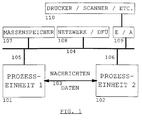
- Part 3 is in this example by the additional devices 107 (mass storage), 108 (network or EDI) and 109 (input / output control, I / O), the peripheral bus connecting these components 104 and the external one connected to I / O 109 Peripherals 110 (printer, scanner, etc.) shown (see claim 1a).
- Process unit one 101 has its own access path 105 with the peripheral bus 104 from part 3 connected (see claim 1d). Is accordingly process unit two 102 also has its own Access path 106 to peripheral bus 104 and thus the shared components 107, 108, 109 and 110 connected from part 3.
- the mutual Occupancy of the peripheral bus 104 through process units one 101 and two 102 can for example by a collision detection method, similar to that used with Ethernet, will be realized.
- peripheral bus 104 The type of access to the individual components 107, 108, 109 and 110 by means of peripheral bus 104, and the selection of components are only examples and do not represent any according to the invention Features. It might as well, for example a crossbar switch can be realized, the simultaneous access of parts 1 and 2 representing process units on the components of Part 3 would allow as long as the targeted Component groups are disjoint.
- process units one 101 and two 102 which are parts 1 and 2 Represent claim 1 is only exemplary.
- a other, more developed design is in Fig. 2 shown.
- the process units are in this drawing with 201 (process unit one, PE1) and 202 (process unit two, PE2), since they are just another possible design represent (see claim 1a, 2, 3, 6, 7).
- PE1 201 is through its own access path 207, that here for example by a SCSI or a IEEE bus could be implemented with one Peripheral bus 206 connected (see claim 1d).
- PE2 202 is not necessarily equivalent 208 also connected to 206.
- As an access device 209 peripheral bus control one, PBK1 and 213 (peripheral bus control two, PBK2) SCSI or IEEE host adapter accepted.
- the connection 203 for the exchange of messages between PBK1 and PBK2 is optional (see claim 8, 9), could but for example through an additional connection between the host adapters or via special Protocols on peripheral bus 206 or via detours, using access paths 204 for data or 205 for messages.
- PBK1 209 is still connected to 210 (memory one, S1) what through direct access control (DMA, direct memory access) to memory S1 can be implemented would be, and with 211 (extension unit one, EE1).
- the EE1 211 includes, for example, adapters for image output 217 (image output device, BAG) or for connection of input devices 218 (input device, EG).
- BAG image output device
- EG input device
- PE2 202 The internal structure of PE2 202 is analogous to that Same.
- PBK2 213 is connected to S2 214 (memory two, S2) and EE2 215 (extension unit two, EE2), which in this example consists of a math coprocessor could exist (see claim 7).
- S2 214 is connected to PBK2 213, EE2 215 and the processor P2 216, which in turn also Has contact with EE2 215.
- P2 216 could be any Be a microprocessor.
- the present invention is easy existing architectures can be adapted by the old architecture part 2, here PE2 202, represents in a suitable manner, for example using one of the methods described to get a Part 1, here PE1 201 supplemented and connected to it can be.
- Components may be used the original architecture, e.g. a Graphics card in which PE1 201 are used.
- connection 204 for data between S1 210 and S2 214 could be implemented as a DMA transfer, which is initiated by processors P1 212 and P2 216 can be.
- Link 205 for messages could be realized through interrupt lines be through which the processors mutually could inform of events that then possibly accompanied by a transfer to 204 would.
- queues could also be used implemented in hardware (for example as a FIFO memory) (see claim 1c, 4).
- connections 203, 204 and 205 are well defined If necessary, the PE1 201 can also later, for example against one in FIG. 3 variant PE1 301 shown can be replaced. Of course, the reverse also applies to one another fictional implementation of PE2 202. Here the possible module concept becomes apparent (see Claim 10).
- PE1 301 from FIG. 3 The basic structure of PE1 301 from FIG. 3 is the same as that of PE1 201.
- P1 302 corresponds to P1 212, but in this case it will be implemented more as a universal processor, since the graphic functions, such as will be explained by other components.
- S1 303 which corresponds to S1 210, but may have different characteristics.
- PBK1 304 which corresponds to PBK1 209.
- P1 302, S1 303 and PBK1 304 all have one or more connections to the rest in PE1 301. This rest represents the equivalent to EE1 211.
- a digital signal processor (DSP) 308 with Connection to S1 303 and interfaces to 312 (audio input device, AEG) and 313 (audio output device, AAG).
- An input process unit EPE 307 which has an interface to one or more EG 311 input devices.
- a video process unit (VPE) 306 which on the one hand has an interface to 309 (image output device, BAG) and 310 (image input device, BEG), but also has access to a scalable number of image process units (BPE1, BPE2, BPE3, ...) 350, 351, 352, ... has.
- the BPEs could consist of a simple graphics processor, possibly with a BITBLT function, and part of the image memory. In parallel, they generate the representation, which is read out by VPE 306 and output as a video signal or arrives at the VPE 306 as a video signal and is distributed by this to the BPEs after conversion.
- the BPEs have individual or group connections with compression-decompression units (KDE1, KDE2, ...) 330, 331, ... which mediate data streams between PBK1 304 and the various KDEs and convert them as desired.
- the PBK1 304 can also consist of several parallel access units, for example, in order to achieve a larger bandwidth.
Landscapes
- Engineering & Computer Science (AREA)
- Theoretical Computer Science (AREA)
- Computer Hardware Design (AREA)
- Physics & Mathematics (AREA)
- General Engineering & Computer Science (AREA)
- General Physics & Mathematics (AREA)
- Computing Systems (AREA)
- Multi Processors (AREA)
- Stored Programmes (AREA)
- Executing Machine-Instructions (AREA)
- Hardware Redundancy (AREA)
- Information Retrieval, Db Structures And Fs Structures Therefor (AREA)
- Digital Computer Display Output (AREA)
Claims (10)
- Système informatique avec interface utilisateur, qui comprend plusieurs unités de processus (101,102), utilise des systèmes de bus internes séparés, comporte des dispositifs de transfert de données et de messages (103) et comprend un logiciel gérant pour tout le système l'interface utilisateur graphique
caractérisé par le faita) que les composants matériels et logiciels du système informatique sont répartis en trois parties de telle sorte qu'une partie 1 (101) se charge des tâches pour la réalisation de l'interface utilisateur en ce qui concerne la représentation et la fonction; qu'une partie 2 (102) prend en charge surtout le déroulement des programmes d'application et ne contient pas des programmes d'exploitation ni de composant nécessaires à l'interface utilisateur; et qu'une partie 3 comprend les composants restants (107, 108, 109, 110) du système informatique ainsi qu'une structure d'accès (104) à ces composants appropriée, les parties 1, 2 et 3 étant réalisées, à part les composants périphériques externes (110), comme une unité d'appareils, qui peut elle-même être modulaire,b) que chacune des parties 1, 2 et 3 possède pour les tâches internes des chemins de données propres, séparés de ceux des autres parties,c) qu'il existe une interface logicielle et matérielle (103) dans l'unité d'appareils entre la partie 1 (101) et la partie 2 (102), qui soutient l'échange de messages et de données, sans établir une liaison directe permanente, qui gênerait le déroulement indépendant des processus dans les parties 1 et 2,d) qu'il existe pour chacune des parties 1 et 2 une liaison directe propre (105, 106) avec les équipements supplémentaires de la partie 3 utilisés en commun. - Système informatique d'après la revendication 1
caractérisé par le fait
que la partie 1 (201) est réalisée par au moins un processeur propre (212) avec mémoire correspondante (210) et dispositif d'accès (209) aux composants de la partie 3 utilisés en commun avec la partie 2 (202). - Système informatique d'après une des revendications précédantes
caractérisé par le fait
que la partie 2 (202) est réalisée par au moins un processeur propre (216) avec mémoire correspondante (214) et dispositif d'accès (213) aux composants de la partie 3 utilisés en commun avec la partie 1 (201). - Système informatique d'après une des revendications précédantes
caractérisé par le fait
que l'interface (103) entre la partie 1 et la partie 2 soutient l'échange efficient de données (204) et de messages (205) grâce à l'utilisation de signaux d'interruption et de files d'attente. - Système informatique d'après une des revendications précédantes
caractérisé par le fait
qu'il existe des chemins d'accès supplémentaires propres, pour la partie 1 et/ou la partie 2, à des composants de la partie 3 affectés en exclusivité à la partie respective. - Système informatique d'après une des revendications précédantes
caractérisé par le fait
qu'il existe des dispositifs (211) supplémentaires propres dans la partie 1, qui soutiennent sa fonction, de préférence pour accélérer l'affichage graphique (350, 351, 352, ...) et/ou pour assister (306, 307, 308) différents périphériques d'entrée/de sortie (309, ..., 313) et/ou des mémoires de masse locales et/ou la compression/décompression de données (330, 331, ...). - Système informatique d'après une des revendications précédantes
caractérisé par le fait
qu'il existe des dispositifs (215) supplémentaires propres dans la partie 2, qui soutiennent la fonction respective, de préférence pour accélérer les fonctions mathématiques et/ou des fonctions de conservation de données, comme la recherche phonétiques dans des textes entiers, et/ou des mémoires de masse locales. - Système informatique d'après une des revendications précédantes
caractérisé par le fait
qu'il existe entre les dispositifs d'accès (209, 213) des parties 1 et 2, qui permettent l'accès aux composants de la partie 3 utilisés en commun, une liaison (203) qui traite, de préférence à l'aide d'une assignation contrôlée par priorités, une collision sur les chemins de données communs, donc l'empêche ou l'utilise délibérément. - Système informatique d'après la revendication 8
caractérisé par le fait
que la liaison (203) est réalisée avec une assignation contrôlée par priorités, qui utilise de préférence des priorités qui peuvent être changées de façon dynamique, pour par exemple modifier la priorité en faveur d'une des deux parties 1 ou 2 par rapport à la configuration de base. - Système informatique d'après une des revendications précédantes
caractérisé par le fait
que les parties 1, 2 et 3 sont réalisées en modules et que les interfaces matérielles et logicielles (103, 105, 106) sont définies de telle sorte qu'elles soutiennent des configurations différentes et/ou de compléter le système en cas de nouveaux besoins.
Applications Claiming Priority (3)
| Application Number | Priority Date | Filing Date | Title |
|---|---|---|---|
| DE4326740 | 1993-08-09 | ||
| DE4326740A DE4326740C1 (de) | 1993-08-09 | 1993-08-09 | Architektur für eine Rechenanlage |
| PCT/DE1994/000848 WO1995004973A1 (fr) | 1993-08-09 | 1994-07-22 | Architecture pour systeme informatique |
Publications (2)
| Publication Number | Publication Date |
|---|---|
| EP0713588A1 EP0713588A1 (fr) | 1996-05-29 |
| EP0713588B1 true EP0713588B1 (fr) | 1999-04-07 |
Family
ID=6494803
Family Applications (1)
| Application Number | Title | Priority Date | Filing Date |
|---|---|---|---|
| EP94921583A Expired - Lifetime EP0713588B1 (fr) | 1993-08-09 | 1994-07-22 | Architecture pour systeme informatique |
Country Status (9)
| Country | Link |
|---|---|
| US (1) | US5842013A (fr) |
| EP (1) | EP0713588B1 (fr) |
| JP (1) | JP4106083B2 (fr) |
| KR (1) | KR100370637B1 (fr) |
| AT (1) | ATE178726T1 (fr) |
| AU (1) | AU7226094A (fr) |
| CA (1) | CA2168741C (fr) |
| DE (3) | DE4326740C1 (fr) |
| WO (1) | WO1995004973A1 (fr) |
Families Citing this family (12)
| Publication number | Priority date | Publication date | Assignee | Title |
|---|---|---|---|---|
| US5999183A (en) * | 1997-07-10 | 1999-12-07 | Silicon Engineering, Inc. | Apparatus for creating a scalable graphics system with efficient memory and bandwidth usage |
| DE60007252T2 (de) * | 1999-03-05 | 2004-09-16 | Amulet Technologies, LLC, Campbell | Graphischer benutzerschnittstellentreiber für eingebettete systeme |
| US7024346B1 (en) | 2000-05-17 | 2006-04-04 | Koninklijke Philips Electronics N.V. | Automatic ATAP test bench generator |
| TW578043B (en) * | 2001-06-18 | 2004-03-01 | Oqo Inc | Modular computing system |
| US20030069943A1 (en) * | 2001-10-04 | 2003-04-10 | International Business Machines Corporation | Method and apparatus for user personalized and adaptive business processing modeling and integration |
| US20060129721A1 (en) * | 2002-06-18 | 2006-06-15 | Betts-Lacroix Jonathan | Modular computing system |
| US20030231168A1 (en) * | 2002-06-18 | 2003-12-18 | Jory Bell | Component for use as a portable computing device and pointing device in a modular computing system |
| DE10233136B4 (de) * | 2002-07-20 | 2005-12-01 | Battenfeld Extrusionstechnik Gmbh | Steuerung für eine Kompaktanlage |
| US7054965B2 (en) * | 2003-03-18 | 2006-05-30 | Oqo Incorporated | Component for use as a portable computing device and pointing device |
| US7317175B2 (en) * | 2003-06-24 | 2008-01-08 | Jere F. Irwin | User interface for configuring and controlling an array of heater elements |
| WO2005067604A2 (fr) * | 2004-01-05 | 2005-07-28 | Oqo Incorporated | Station d'accueil pour dispositif informatique mobile |
| DE102019106410A1 (de) * | 2019-03-13 | 2020-09-17 | Liebherr-Aerospace Lindenberg Gmbh | Vorrichtung und Verfahren zur Datenübertragung |
Citations (1)
| Publication number | Priority date | Publication date | Assignee | Title |
|---|---|---|---|---|
| EP0528396A2 (fr) * | 1991-08-21 | 1993-02-24 | International Business Machines Corporation | Procédé de commande d'un processus industriel |
Family Cites Families (9)
| Publication number | Priority date | Publication date | Assignee | Title |
|---|---|---|---|---|
| CA1183609A (fr) * | 1982-03-29 | 1985-03-05 | Bruce S. Allen | Interface homme-machine |
| US4570220A (en) * | 1983-11-25 | 1986-02-11 | Intel Corporation | High speed parallel bus and data transfer method |
| DE3689053D1 (de) * | 1985-06-14 | 1993-10-28 | Siemens Ag | Verfahren zum Betrieb einer Datenverarbeitungsanlage. |
| US4831520A (en) * | 1987-02-24 | 1989-05-16 | Digital Equipment Corporation | Bus interface circuit for digital data processor |
| EP0350911A3 (fr) * | 1988-07-13 | 1990-09-05 | Modular Computer Systems Inc. | Structure multiprocesseur à couplage rigide pour une application en temps réel |
| US4897779A (en) * | 1988-07-20 | 1990-01-30 | Digital Equipment Corporation | Method and apparatus for optimizing inter-processor instruction transfers |
| US5179660A (en) * | 1989-05-15 | 1993-01-12 | International Business Machines Incorporated | System for reducing communications overhead in distributed database transactions by serializing in order related requests into single transmission message and receiving transmission response |
| EP0401803A3 (fr) * | 1989-06-06 | 1992-01-22 | Comtrol Corporation | Multiplicité de postes de travail graphique à distance |
| ES2063087T3 (es) * | 1989-08-16 | 1995-01-01 | Siemens Ag | Sistema de automatizacion flexible para procesos industriales variables. |
-
1993
- 1993-08-09 DE DE4326740A patent/DE4326740C1/de not_active Revoked
-
1994
- 1994-07-22 US US08/596,127 patent/US5842013A/en not_active Expired - Lifetime
- 1994-07-22 DE DE4495764T patent/DE4495764D2/de not_active Expired - Fee Related
- 1994-07-22 WO PCT/DE1994/000848 patent/WO1995004973A1/fr not_active Ceased
- 1994-07-22 DE DE59408088T patent/DE59408088D1/de not_active Expired - Lifetime
- 1994-07-22 AT AT94921583T patent/ATE178726T1/de not_active IP Right Cessation
- 1994-07-22 CA CA002168741A patent/CA2168741C/fr not_active Expired - Fee Related
- 1994-07-22 EP EP94921583A patent/EP0713588B1/fr not_active Expired - Lifetime
- 1994-07-22 JP JP50613695A patent/JP4106083B2/ja not_active Expired - Fee Related
- 1994-07-22 KR KR1019960700663A patent/KR100370637B1/ko not_active Expired - Fee Related
- 1994-07-22 AU AU72260/94A patent/AU7226094A/en not_active Abandoned
Patent Citations (1)
| Publication number | Priority date | Publication date | Assignee | Title |
|---|---|---|---|---|
| EP0528396A2 (fr) * | 1991-08-21 | 1993-02-24 | International Business Machines Corporation | Procédé de commande d'un processus industriel |
Also Published As
| Publication number | Publication date |
|---|---|
| DE4495764D2 (de) | 1996-10-17 |
| AU7226094A (en) | 1995-02-28 |
| KR100370637B1 (ko) | 2003-03-15 |
| DE4326740C1 (de) | 1994-10-13 |
| KR960704275A (ko) | 1996-08-31 |
| DE59408088D1 (de) | 1999-05-12 |
| JPH09501524A (ja) | 1997-02-10 |
| WO1995004973A1 (fr) | 1995-02-16 |
| US5842013A (en) | 1998-11-24 |
| CA2168741C (fr) | 2005-05-31 |
| JP4106083B2 (ja) | 2008-06-25 |
| ATE178726T1 (de) | 1999-04-15 |
| CA2168741A1 (fr) | 1995-02-16 |
| EP0713588A1 (fr) | 1996-05-29 |
Similar Documents
| Publication | Publication Date | Title |
|---|---|---|
| DE69228960T2 (de) | Vermittlungsnetz für Prozessoren | |
| DE69319544T2 (de) | Verfahren und Vorrichtung zum stufenweisen Abbau von Videodaten | |
| DE69519926T2 (de) | Verfahren und vorrichtung zum einhalten der transaktionssteuerung und zur unterstützung von verzögerten antworten in einer busbrücke | |
| DE69720477T2 (de) | Von einem media-koprozessor auf gemeinsamem speicher einer workstation ausgeführtes kompressions- und dekompressionsschema | |
| DE69229473T2 (de) | Verfahren und vorrichtung zum puffern von daten in nachrichtennetzwerkstationen | |
| DE69422324T2 (de) | Speicherarchitektur mit Fenstern zum Bildkompilieren | |
| DE68927375T2 (de) | Arbitrierung von Übertragungsanforderungen in einem Multiprozessor-Rechnersystem | |
| DE3751091T2 (de) | Übertragungsprotokoll zwischen Prozessoren. | |
| DE69313191T2 (de) | Architektur einer skalierbaren Multimedienplattform | |
| DE69030861T2 (de) | Bus-Master-Steuerprotokoll | |
| DE69131971T2 (de) | Netzwerkanpassungseinrichtung mit Puffer und Mehrbeschreibungskreis | |
| DE69029892T2 (de) | Datendarstellung und Protokoll | |
| DE69229716T2 (de) | Schaltungsarchitektur zum mehrkanaligen DMA-Betrieb | |
| DE4121446C2 (de) | Terminal-Server-Architektur | |
| EP0713588B1 (fr) | Architecture pour systeme informatique | |
| DE3642324C2 (de) | Multiprozessoranlage mit Prozessor-Zugriffssteuerung | |
| DE69520886T2 (de) | System und verfahren zur verarbeitung von signaldaten und kommunikationssystem mit system zur verarbeitung von signaldaten | |
| DE60038703T2 (de) | Asynchrone Datenübertragung | |
| DE2104733A1 (de) | Mehrkanal Ubertragungsverarbeitungs system zum unabhängigen Steuern von Ein gäbe/Ausgabe Datenübertragungen | |
| DE2134402B2 (de) | Vorrichtung zum Abfragen der Verfügbarkeit eines Kommunikationsweges zu einer Eingabe-Ausgabeeinheit | |
| DE69328865T2 (de) | Virtuelle funkschnittstelle | |
| DE68927795T2 (de) | Übertragungssystem mit einem gemeinsamen Speicher | |
| DE60217132T2 (de) | Vorrichtung zur erhaltung der producer-consumer anordnung entlang einer ungeordneten schnittstelle | |
| EP0184706B1 (fr) | Montage d'interface | |
| DE69735546T2 (de) | Paketvermittelte leitweglenkung-architektur für mehrere gleichzeitige verbindungen |
Legal Events
| Date | Code | Title | Description |
|---|---|---|---|
| PUAI | Public reference made under article 153(3) epc to a published international application that has entered the european phase |
Free format text: ORIGINAL CODE: 0009012 |
|
| 17P | Request for examination filed |
Effective date: 19960307 |
|
| AK | Designated contracting states |
Kind code of ref document: A1 Designated state(s): AT CH DE ES FR GB IE IT LI NL SE |
|
| GRAG | Despatch of communication of intention to grant |
Free format text: ORIGINAL CODE: EPIDOS AGRA |
|
| 17Q | First examination report despatched |
Effective date: 19980113 |
|
| GRAG | Despatch of communication of intention to grant |
Free format text: ORIGINAL CODE: EPIDOS AGRA |
|
| GRAH | Despatch of communication of intention to grant a patent |
Free format text: ORIGINAL CODE: EPIDOS IGRA |
|
| GRAH | Despatch of communication of intention to grant a patent |
Free format text: ORIGINAL CODE: EPIDOS IGRA |
|
| GRAA | (expected) grant |
Free format text: ORIGINAL CODE: 0009210 |
|
| AK | Designated contracting states |
Kind code of ref document: B1 Designated state(s): AT CH DE ES FR GB IE IT LI NL SE |
|
| PG25 | Lapsed in a contracting state [announced via postgrant information from national office to epo] |
Ref country code: SE Free format text: THE PATENT HAS BEEN ANNULLED BY A DECISION OF A NATIONAL AUTHORITY Effective date: 19990407 Ref country code: NL Free format text: LAPSE BECAUSE OF FAILURE TO SUBMIT A TRANSLATION OF THE DESCRIPTION OR TO PAY THE FEE WITHIN THE PRESCRIBED TIME-LIMIT Effective date: 19990407 Ref country code: IT Free format text: LAPSE BECAUSE OF FAILURE TO SUBMIT A TRANSLATION OF THE DESCRIPTION OR TO PAY THE FEE WITHIN THE PRESCRIBED TIME-LIMIT;WARNING: LAPSES OF ITALIAN PATENTS WITH EFFECTIVE DATE BEFORE 2007 MAY HAVE OCCURRED AT ANY TIME BEFORE 2007. THE CORRECT EFFECTIVE DATE MAY BE DIFFERENT FROM THE ONE RECORDED. Effective date: 19990407 Ref country code: ES Free format text: THE PATENT HAS BEEN ANNULLED BY A DECISION OF A NATIONAL AUTHORITY Effective date: 19990407 |
|
| REF | Corresponds to: |
Ref document number: 178726 Country of ref document: AT Date of ref document: 19990415 Kind code of ref document: T |
|
| REG | Reference to a national code |
Ref country code: CH Ref legal event code: EP |
|
| REG | Reference to a national code |
Ref country code: IE Ref legal event code: FG4D Free format text: GERMAN |
|
| REF | Corresponds to: |
Ref document number: 59408088 Country of ref document: DE Date of ref document: 19990512 |
|
| PG25 | Lapsed in a contracting state [announced via postgrant information from national office to epo] |
Ref country code: AT Free format text: LAPSE BECAUSE OF NON-PAYMENT OF DUE FEES Effective date: 19990722 |
|
| PG25 | Lapsed in a contracting state [announced via postgrant information from national office to epo] |
Ref country code: LI Free format text: LAPSE BECAUSE OF NON-PAYMENT OF DUE FEES Effective date: 19990731 Ref country code: CH Free format text: LAPSE BECAUSE OF NON-PAYMENT OF DUE FEES Effective date: 19990731 |
|
| GBT | Gb: translation of ep patent filed (gb section 77(6)(a)/1977) |
Effective date: 19990708 |
|
| ET | Fr: translation filed | ||
| NLV1 | Nl: lapsed or annulled due to failure to fulfill the requirements of art. 29p and 29m of the patents act | ||
| PG25 | Lapsed in a contracting state [announced via postgrant information from national office to epo] |
Ref country code: IE Free format text: LAPSE BECAUSE OF NON-PAYMENT OF DUE FEES Effective date: 19991206 |
|
| REG | Reference to a national code |
Ref country code: IE Ref legal event code: FD4D |
|
| PLBE | No opposition filed within time limit |
Free format text: ORIGINAL CODE: 0009261 |
|
| STAA | Information on the status of an ep patent application or granted ep patent |
Free format text: STATUS: NO OPPOSITION FILED WITHIN TIME LIMIT |
|
| REG | Reference to a national code |
Ref country code: CH Ref legal event code: PL |
|
| 26N | No opposition filed | ||
| REG | Reference to a national code |
Ref country code: GB Ref legal event code: IF02 |
|
| PGFP | Annual fee paid to national office [announced via postgrant information from national office to epo] |
Ref country code: FR Payment date: 20100728 Year of fee payment: 17 Ref country code: DE Payment date: 20100712 Year of fee payment: 17 |
|
| PGFP | Annual fee paid to national office [announced via postgrant information from national office to epo] |
Ref country code: GB Payment date: 20100712 Year of fee payment: 17 |
|
| GBPC | Gb: european patent ceased through non-payment of renewal fee |
Effective date: 20110722 |
|
| REG | Reference to a national code |
Ref country code: FR Ref legal event code: ST Effective date: 20120330 |
|
| PG25 | Lapsed in a contracting state [announced via postgrant information from national office to epo] |
Ref country code: DE Free format text: LAPSE BECAUSE OF NON-PAYMENT OF DUE FEES Effective date: 20120201 Ref country code: FR Free format text: LAPSE BECAUSE OF NON-PAYMENT OF DUE FEES Effective date: 20110801 |
|
| REG | Reference to a national code |
Ref country code: DE Ref legal event code: R119 Ref document number: 59408088 Country of ref document: DE Effective date: 20120201 |
|
| PG25 | Lapsed in a contracting state [announced via postgrant information from national office to epo] |
Ref country code: GB Free format text: LAPSE BECAUSE OF NON-PAYMENT OF DUE FEES Effective date: 20110722 |