EP0715005B1 - Dispositif et procédé pour produire un monocristal - Google Patents
Dispositif et procédé pour produire un monocristal Download PDFInfo
- Publication number
- EP0715005B1 EP0715005B1 EP95118840A EP95118840A EP0715005B1 EP 0715005 B1 EP0715005 B1 EP 0715005B1 EP 95118840 A EP95118840 A EP 95118840A EP 95118840 A EP95118840 A EP 95118840A EP 0715005 B1 EP0715005 B1 EP 0715005B1
- Authority
- EP
- European Patent Office
- Prior art keywords
- melt
- single crystal
- inert gas
- recipient
- receiver chamber
- Prior art date
- Legal status (The legal status is an assumption and is not a legal conclusion. Google has not performed a legal analysis and makes no representation as to the accuracy of the status listed.)
- Expired - Lifetime
Links
- 239000013078 crystal Substances 0.000 title claims description 53
- 238000000034 method Methods 0.000 title claims description 13
- 239000000155 melt Substances 0.000 claims description 36
- 239000011261 inert gas Substances 0.000 claims description 16
- XUIMIQQOPSSXEZ-UHFFFAOYSA-N Silicon Chemical compound [Si] XUIMIQQOPSSXEZ-UHFFFAOYSA-N 0.000 claims description 12
- 229910052710 silicon Inorganic materials 0.000 claims description 12
- 239000010703 silicon Substances 0.000 claims description 12
- 239000002019 doping agent Substances 0.000 description 11
- 238000004519 manufacturing process Methods 0.000 description 9
- LIVNPJMFVYWSIS-UHFFFAOYSA-N silicon monoxide Chemical compound [Si-]#[O+] LIVNPJMFVYWSIS-UHFFFAOYSA-N 0.000 description 8
- QVGXLLKOCUKJST-UHFFFAOYSA-N atomic oxygen Chemical compound [O] QVGXLLKOCUKJST-UHFFFAOYSA-N 0.000 description 5
- 229910052760 oxygen Inorganic materials 0.000 description 5
- 239000001301 oxygen Substances 0.000 description 5
- 229910052787 antimony Inorganic materials 0.000 description 4
- WATWJIUSRGPENY-UHFFFAOYSA-N antimony atom Chemical compound [Sb] WATWJIUSRGPENY-UHFFFAOYSA-N 0.000 description 4
- 229910052785 arsenic Inorganic materials 0.000 description 4
- RQNWIZPPADIBDY-UHFFFAOYSA-N arsenic atom Chemical compound [As] RQNWIZPPADIBDY-UHFFFAOYSA-N 0.000 description 4
- 239000007789 gas Substances 0.000 description 3
- ZOXJGFHDIHLPTG-UHFFFAOYSA-N Boron Chemical compound [B] ZOXJGFHDIHLPTG-UHFFFAOYSA-N 0.000 description 1
- OAICVXFJPJFONN-UHFFFAOYSA-N Phosphorus Chemical compound [P] OAICVXFJPJFONN-UHFFFAOYSA-N 0.000 description 1
- 230000002730 additional effect Effects 0.000 description 1
- 229910052796 boron Inorganic materials 0.000 description 1
- 238000002425 crystallisation Methods 0.000 description 1
- 230000008025 crystallization Effects 0.000 description 1
- 230000003247 decreasing effect Effects 0.000 description 1
- 230000006735 deficit Effects 0.000 description 1
- 238000009434 installation Methods 0.000 description 1
- 239000007788 liquid Substances 0.000 description 1
- 239000012768 molten material Substances 0.000 description 1
- 229910052698 phosphorus Inorganic materials 0.000 description 1
- 239000011574 phosphorus Substances 0.000 description 1
- 239000002244 precipitate Substances 0.000 description 1
- 239000000047 product Substances 0.000 description 1
- 230000005855 radiation Effects 0.000 description 1
- 239000007787 solid Substances 0.000 description 1
Images


Classifications
-
- C—CHEMISTRY; METALLURGY
- C30—CRYSTAL GROWTH
- C30B—SINGLE-CRYSTAL GROWTH; UNIDIRECTIONAL SOLIDIFICATION OF EUTECTIC MATERIAL OR UNIDIRECTIONAL DEMIXING OF EUTECTOID MATERIAL; REFINING BY ZONE-MELTING OF MATERIAL; PRODUCTION OF A HOMOGENEOUS POLYCRYSTALLINE MATERIAL WITH DEFINED STRUCTURE; SINGLE CRYSTALS OR HOMOGENEOUS POLYCRYSTALLINE MATERIAL WITH DEFINED STRUCTURE; AFTER-TREATMENT OF SINGLE CRYSTALS OR A HOMOGENEOUS POLYCRYSTALLINE MATERIAL WITH DEFINED STRUCTURE; APPARATUS THEREFOR
- C30B29/00—Single crystals or homogeneous polycrystalline material with defined structure characterised by the material or by their shape
- C30B29/02—Elements
- C30B29/06—Silicon
-
- C—CHEMISTRY; METALLURGY
- C30—CRYSTAL GROWTH
- C30B—SINGLE-CRYSTAL GROWTH; UNIDIRECTIONAL SOLIDIFICATION OF EUTECTIC MATERIAL OR UNIDIRECTIONAL DEMIXING OF EUTECTOID MATERIAL; REFINING BY ZONE-MELTING OF MATERIAL; PRODUCTION OF A HOMOGENEOUS POLYCRYSTALLINE MATERIAL WITH DEFINED STRUCTURE; SINGLE CRYSTALS OR HOMOGENEOUS POLYCRYSTALLINE MATERIAL WITH DEFINED STRUCTURE; AFTER-TREATMENT OF SINGLE CRYSTALS OR A HOMOGENEOUS POLYCRYSTALLINE MATERIAL WITH DEFINED STRUCTURE; APPARATUS THEREFOR
- C30B15/00—Single-crystal growth by pulling from a melt, e.g. Czochralski method
- C30B15/14—Heating of the melt or the crystallised materials
-
- Y—GENERAL TAGGING OF NEW TECHNOLOGICAL DEVELOPMENTS; GENERAL TAGGING OF CROSS-SECTIONAL TECHNOLOGIES SPANNING OVER SEVERAL SECTIONS OF THE IPC; TECHNICAL SUBJECTS COVERED BY FORMER USPC CROSS-REFERENCE ART COLLECTIONS [XRACs] AND DIGESTS
- Y10—TECHNICAL SUBJECTS COVERED BY FORMER USPC
- Y10T—TECHNICAL SUBJECTS COVERED BY FORMER US CLASSIFICATION
- Y10T117/00—Single-crystal, oriented-crystal, and epitaxy growth processes; non-coating apparatus therefor
- Y10T117/10—Apparatus
- Y10T117/1024—Apparatus for crystallization from liquid or supercritical state
- Y10T117/1076—Apparatus for crystallization from liquid or supercritical state having means for producing a moving solid-liquid-solid zone
- Y10T117/1088—Apparatus for crystallization from liquid or supercritical state having means for producing a moving solid-liquid-solid zone including heating or cooling details
Definitions
- the invention relates to an apparatus and a method for Production of a single crystal from silicon after the Czochralski method.
- An essential feature of this method is that a monocrystalline seed crystal in one from the environment sealed recipients with molten material, that is in a crucible, brought in contact and pulled away from the melt at a certain speed with a single crystal growing on its underside begins.
- Many drawing systems are growing with one Single crystal shielding, tubular to conical body fitted.
- US-4,330,362 is a Single crystal shielding body described, which to the Melt tapered towards it, giving it a pot-like appearance gives.
- Such the growing single crystal over his entire length or part of it concentrically enclosing Bodies shield heat radiation emanating from the crucible wall, from.
- the single crystal has a higher speed can be pulled.
- EP-340 941 A1 describes a shielding of the single crystal Shown body that has an opening through the silicon is recharged to the crucible.
- silicon monoxide continuously becomes formed that as a gas in the recipient room above the melt escapes.
- the recipient is filled with inert gas rinsed to prevent the silicon monoxide from adhering cold parts in the crucible area of the drawing system as Precipitate solid, to the crystallization front at the single crystal reach and cause dislocations in the crystal. It is common to pass inert gas to the surface of the melt and together with the resulting silicon monoxide from the recipient suck off.
- a body shielding the single crystal divides the recipient space above the melt into an inner one and an outer part.
- An inert gas stream for removal Silicon monoxide is usually through the inner part of the recipient space to the surface of the melt. He then gets between the lower end of the shielding body and the surface of the melt in the outer part of the recipient space and finally to one provided in the recipient wall Suction opening.
- the object of the invention described below was therefore in the manufacture of single crystals from silicon to improve by the Czochralski method so that even single crystals with high arsenic or antimony content without difficulty and can be produced with good yield.
- the present invention relates to a device for Production of a single crystal from silicon after the Czochralski method, with one with Inert gas-flushable recipient, one housed therein Crucible for holding a melt, a device for drawing a single crystal from the melt and one, the growing one Single crystal shielding, tubular to conical body, at its lower end as an annular shielding screen is formed and the recipient space above the melt into one separates inner part and an outer part, whereby inert gas, which leads to the melt in the inner part of the recipient space will, between the lower end of the body and the Surface of the melt in the outer part of the recipient space arrives, which is characterized in that the body has a side wall with at least one opening, through the inert gas directly from the inner part to the outer part of the Can reach recipient space, and the opening in the lower half of the side wall of the body.
- the proposed procedural and device changes to accommodate those previously encountered Difficulties in producing highly antimony or arsenic doped To bypass single crystals of silicon.
- the invention is particularly suitable for the production of single crystals with diameters
- An advantage of over 100 mm because the melt is from the single crystal is pulled, not as before, over the degree of saturation must also be concentrated with dopant.
- the process also incorporates oxygen influenced in the single crystal and therefore general important for the production of silicon single crystals is. This additional effect is independent of the type and the amount of deliberately added dopants and occurs for example when doping with boron or phosphorus on. It expresses itself in the fact that in the finished single crystal measured oxygen content depending on the number and the size of the openings varies.
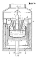
- Figures la) -d) each show one Longitudinal section through a plant for the production of single crystals according to the Czochralski method. It is only for Understanding the invention necessary features shown.
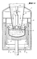
- Figures 2a) -h) show longitudinal sections through preferred Embodiments of the single crystal shielding body. Identical reference numbers used in different figures refer to the same device features.
- the invention Device consists of a recipient 1, the one with molten silicon and optionally added Dopant filled crucible 2 houses. From the melt 3 becomes a single crystal 5 with the aid of a pulling device 4 drawn.
- the single crystal is of a shielding, rotationally symmetrical body 6, which enclosed the recipient space above the melt into an inner part 7 and divides an outer part 8.
- the distance between that lower end 9 of the body and the surface 10 of the melt is preferably 5 to 50 mm, so that inert gas as indicated in the figures la) -d) by arrows, in the inner part 7 of the recipient space is passed through Space between the lower end 9 of the body and the Surface 10 of the melt in the outer part 8 of the recipient space can reach.
- the further path of the inert gas flow from the outer part 8 of the recipient space to one or several suction openings 11 in the wall of the recipient is also indicated with arrows.
- the single crystal shielding body 6 may have a tubular or conical shape.
- the distance between the Single crystal and the inner wall of the body to the bottom End of the body getting shorter.
- this distance remains unchanged over the entire height of the body.
- the height of the body is related to that present invention of minor importance, provided that a certain minimum height is exceeded and ensured is that the particularly hot areas of growing Single crystal to be shielded by the body.
- the body shown in Figure 1d) 6 extends the body shown in Figure 1d) 6 from the upper limit of the recipient 1 to the Crucible 2.
- the present invention it is the single crystal surrounding side wall of the body is not completely closed, but at least points in its lower half an opening 12 through which the in the inner part of the recipient space inert gas stream directed to the surface 10 of the melt partly directly in the outer part 8 of the recipient space reached. Due to the total area of the opening, a certain division ratio with which the Inert gas stream is divided into sub-streams, the inner Part 7 of the recipient room in different ways leave.
- the opening 12 in Body 6 from a variety of slots that are regular Distances are arranged around the circumference of the body.
- Especially preferred embodiments of the single crystal shielding Bodies are shown in Figures 2a) -h).
- a slot 12 is proposed, the follows a circumferential line of the body and only by fastening struts 13 who wear the lower part of the body is interrupted. You can also have two or more on top of each other arranged slots may be provided.
- the preferred Slot width is 5 to 50 mm.
- the lower end of the Single crystal shielding body is designed as an annular shield 14, the is spaced parallel to the surface of the melt.
- the embodiments according to Figure 2 a), d), e) and h) differentiate different from the other embodiments shown of the slot 12 relative to the surface of the shield.
- the design of the shield can also Influence on the flow conditions in the recipient space above be taken from the melt. It is preferred that the inner Edge 15 of the shielding panel in the inner part of the recipient space protrudes and reaches 10 to 80 mm to the single crystal.
- the outer diameter of the shield can be chosen be that the shield with its outer edge 16th protrudes into the outer recipient space and for example 10 to 80 mm to the inner wall of the crucible. The outside diameter however, the shield should not be made smaller are called the outer diameter of the cylindrical or cone-shaped part of the body that is on the surface of the Shielding screen rests (embodiments according to FIG. 2 c) and g)) or to this surface (embodiments according to Figure 2 d) and h)).
Landscapes
- Chemical & Material Sciences (AREA)
- Engineering & Computer Science (AREA)
- Crystallography & Structural Chemistry (AREA)
- Materials Engineering (AREA)
- Metallurgy (AREA)
- Organic Chemistry (AREA)
- Crystals, And After-Treatments Of Crystals (AREA)
- Liquid Deposition Of Substances Of Which Semiconductor Devices Are Composed (AREA)
Claims (3)
- Dispositif pour produire un monocristal de silicium suivant le procédé Czochralski, avec un récipient pouvant être purgé par du gaz inerte, un creuset qui y est logé pour recevoir de la matière en fusion, un dispositif pour tirer un monocristal à partir de la matière en fusion et un corps tubulaire à conique, protégeant le monocristal croissant, qui se présente à son extrémité inférieure sous la forme d'un écran protecteur annulaire et qui sépare la chambre du récipient au-dessus de la matière en fusion en une partie intérieure et une partie extérieure, le gaz inerte, qui est amené dans la partie intérieure de la chambre du récipient vers la matière en fusion, passant entre l'extrémité inférieure du corps et la surface de la matière en fusion dans la partie extérieure de la chambre du récipient, caractérisé en ce que le corps comprend une paroi latérale pourvue d'au moins un orifice, par lequel le gaz inerte peut directement passer de la partie intérieure à la partie extérieure de la chambre du récipient, et l'orifice se trouve dans la moitié inférieure de la paroi latérale du corps.
- Dispositif suivant la revendication 1, caractérisé en ce que l'orifice est formé dans la paroi latérale du corps sous forme de fente qui suit une ligne de circonférence du corps.
- Procédé pour produire un monocristal de silicium suivant le procédé Czochralski, comprenant :le tirage d'un monocristal dans un récipient à partir d'une matière en fusion préparée dans un creuset, le monocristal étant entouré d'un corps tubulaire à conique qui le protège, et qui sépare la chambre du récipient au-dessus de la matière en fusion en une partie intérieure et une partie extérieure;l'amenée d'un flux de gaz inerte par la partie intérieure de la chambre du récipient vers la surface de la matière en fusion et entre l'extrémité inférieure du corps, qui se présente sous la forme d'un écran protecteur annulaire, et la surface de la matière en fusion dans la partie extérieure de la chambre du récipient, caractérisé en cequ'une partie du flux de gaz inerte est amenée, par au moins un orifice dans la moitié inférieure de la paroi latérale du corps, directement de la partie intérieure dans la partie extérieure de la chambre du récipient.
Applications Claiming Priority (2)
| Application Number | Priority Date | Filing Date | Title |
|---|---|---|---|
| DE4442829A DE4442829A1 (de) | 1994-12-01 | 1994-12-01 | Vorrichtung und Verfahren zur Herstellung eines Einkristalls |
| DE4442829 | 1994-12-01 |
Publications (2)
| Publication Number | Publication Date |
|---|---|
| EP0715005A1 EP0715005A1 (fr) | 1996-06-05 |
| EP0715005B1 true EP0715005B1 (fr) | 1999-03-17 |
Family
ID=6534669
Family Applications (1)
| Application Number | Title | Priority Date | Filing Date |
|---|---|---|---|
| EP95118840A Expired - Lifetime EP0715005B1 (fr) | 1994-12-01 | 1995-11-30 | Dispositif et procédé pour produire un monocristal |
Country Status (9)
| Country | Link |
|---|---|
| US (1) | US5578123A (fr) |
| EP (1) | EP0715005B1 (fr) |
| JP (1) | JP2855098B2 (fr) |
| KR (1) | KR0185467B1 (fr) |
| CN (1) | CN1044921C (fr) |
| DE (2) | DE4442829A1 (fr) |
| MY (1) | MY112189A (fr) |
| RU (1) | RU2102539C1 (fr) |
| TW (1) | TW302497B (fr) |
Families Citing this family (20)
| Publication number | Priority date | Publication date | Assignee | Title |
|---|---|---|---|---|
| JPH0859386A (ja) * | 1994-08-22 | 1996-03-05 | Mitsubishi Materials Corp | 半導体単結晶育成装置 |
| DE19546987A1 (de) * | 1995-12-15 | 1997-06-19 | Wacker Siltronic Halbleitermat | Verfahren und Vorrichtung zum Ziehen eines Einkristalls |
| JP3653647B2 (ja) * | 1996-05-31 | 2005-06-02 | イビデン株式会社 | シリコン単結晶引き上げ装置用の保温筒 |
| DE19628851A1 (de) * | 1996-07-17 | 1998-01-22 | Wacker Siltronic Halbleitermat | Verfahren und Vorrichtung zur Herstellung eines Einkristalls |
| JPH10101482A (ja) * | 1996-10-01 | 1998-04-21 | Komatsu Electron Metals Co Ltd | 単結晶シリコンの製造装置および製造方法 |
| US5904768A (en) * | 1996-10-15 | 1999-05-18 | Memc Electronic Materials, Inc. | Process for controlling the oxygen content in silicon wafers heavily doped with antimony or arsenic |
| US6485807B1 (en) | 1997-02-13 | 2002-11-26 | Samsung Electronics Co., Ltd. | Silicon wafers having controlled distribution of defects, and methods of preparing the same |
| SG64470A1 (en) | 1997-02-13 | 1999-04-27 | Samsung Electronics Co Ltd | Methods of manufacturing monocrystalline silicon ingots and wafers by controlling pull rate profiles in a hot zone furnace and ingots and wafers manufactured thereby |
| US6503594B2 (en) | 1997-02-13 | 2003-01-07 | Samsung Electronics Co., Ltd. | Silicon wafers having controlled distribution of defects and slip |
| US5911825A (en) * | 1997-09-30 | 1999-06-15 | Seh America, Inc. | Low oxygen heater |
| JP3267225B2 (ja) * | 1997-12-26 | 2002-03-18 | 住友金属工業株式会社 | 単結晶引き上げ方法、及び単結晶引き上げ装置 |
| JP4776065B2 (ja) * | 2000-09-19 | 2011-09-21 | Sumco Techxiv株式会社 | Cz法単結晶引上げ装置 |
| UA72795C2 (en) * | 2002-09-10 | 2005-04-15 | Pillar Closed Joint Stock Comp | An apparatus for growing monocrystals of silicon, screening device therefor and a method for growing monocrystals using czochralski method |
| RU2241079C1 (ru) * | 2003-06-17 | 2004-11-27 | Федеральное государственное унитарное предприятие "Научно-исследовательский институт Научно-производственное объединение "Луч" | Устройство для выращивания монокристалла кремния из расплава |
| US8152921B2 (en) * | 2006-09-01 | 2012-04-10 | Okmetic Oyj | Crystal manufacturing |
| EP2270264B1 (fr) * | 2009-05-13 | 2011-12-28 | Siltronic AG | Procédé et appareil de croissance de silicium monocristallin à partir d'une coulée |
| CN101914808A (zh) * | 2010-07-19 | 2010-12-15 | 常州天合光能有限公司 | 可消除挥发份在热屏外侧沉积的单晶炉热场 |
| CN107075717B (zh) | 2014-09-19 | 2020-06-16 | 各星有限公司 | 用于防止熔体污染的拉晶机 |
| RU2663130C1 (ru) * | 2018-02-12 | 2018-08-01 | Акционерное общество "Управляющая компания "АКЦЕНТ" | Способ выращивания монокристалла кремния из расплава |
| DE102018217509A1 (de) * | 2018-10-12 | 2020-04-16 | Siltronic Ag | Vorrichtung zum Ziehen eines Einkristalls aus Halbleitermaterial nach der CZ-Methode aus einer Schmelze und Verfahren unter Verwendung der Vorrichtung |
Family Cites Families (9)
| Publication number | Priority date | Publication date | Assignee | Title |
|---|---|---|---|---|
| DE2821481C2 (de) * | 1978-05-17 | 1985-12-05 | Wacker-Chemitronic Gesellschaft für Elektronik-Grundstoffe mbH, 8263 Burghausen | Vorrichtung zum Ziehen von hochreinen Halbleiterstäben aus der Schmelze |
| DE3005492C2 (de) * | 1980-02-14 | 1983-10-27 | Wacker-Chemitronic Gesellschaft für Elektronik-Grundstoffe mbH, 8263 Burghausen | Verfahren zur Herstellung reinster Einkristalle durch Tiegelziehen nach Czochralski |
| JPH0639352B2 (ja) * | 1987-09-11 | 1994-05-25 | 信越半導体株式会社 | 単結晶の製造装置 |
| EP0340941A1 (fr) * | 1988-04-28 | 1989-11-08 | Nkk Corporation | Procédé et appareillage pour la production de monocristaux de silicium |
| JP2686460B2 (ja) * | 1990-03-12 | 1997-12-08 | 住友シチックス株式会社 | 単結晶製造方法 |
| US5363796A (en) * | 1991-02-20 | 1994-11-15 | Sumitomo Metal Industries, Ltd. | Apparatus and method of growing single crystal |
| JP2795036B2 (ja) * | 1992-02-04 | 1998-09-10 | 信越半導体株式会社 | 単結晶引上装置 |
| JP2952733B2 (ja) * | 1992-10-09 | 1999-09-27 | コマツ電子金属株式会社 | シリコン単結晶製造方法 |
| JP2807609B2 (ja) * | 1993-01-28 | 1998-10-08 | 三菱マテリアルシリコン株式会社 | 単結晶の引上装置 |
-
1994
- 1994-12-01 DE DE4442829A patent/DE4442829A1/de not_active Withdrawn
-
1995
- 1995-09-26 TW TW084110074A patent/TW302497B/zh not_active IP Right Cessation
- 1995-10-10 US US08/541,341 patent/US5578123A/en not_active Expired - Lifetime
- 1995-10-25 MY MYPI95003202A patent/MY112189A/en unknown
- 1995-11-20 CN CN95117532A patent/CN1044921C/zh not_active Expired - Lifetime
- 1995-11-28 KR KR1019950044146A patent/KR0185467B1/ko not_active Expired - Lifetime
- 1995-11-30 RU RU95121442A patent/RU2102539C1/ru active
- 1995-11-30 DE DE59505372T patent/DE59505372D1/de not_active Expired - Lifetime
- 1995-11-30 EP EP95118840A patent/EP0715005B1/fr not_active Expired - Lifetime
- 1995-12-01 JP JP7335638A patent/JP2855098B2/ja not_active Expired - Fee Related
Also Published As
| Publication number | Publication date |
|---|---|
| JPH08225397A (ja) | 1996-09-03 |
| EP0715005A1 (fr) | 1996-06-05 |
| US5578123A (en) | 1996-11-26 |
| CN1044921C (zh) | 1999-09-01 |
| TW302497B (fr) | 1997-04-11 |
| CN1129747A (zh) | 1996-08-28 |
| DE4442829A1 (de) | 1996-06-05 |
| KR0185467B1 (ko) | 1999-04-15 |
| MY112189A (en) | 2001-04-30 |
| KR960023271A (ko) | 1996-07-18 |
| DE59505372D1 (de) | 1999-04-22 |
| RU2102539C1 (ru) | 1998-01-20 |
| JP2855098B2 (ja) | 1999-02-10 |
Similar Documents
| Publication | Publication Date | Title |
|---|---|---|
| EP0715005B1 (fr) | Dispositif et procédé pour produire un monocristal | |
| DE69802707T2 (de) | Hitzeschild für eine kristallziehungsvorrichtung | |
| DE69410835T2 (de) | Anlage zum Ziehen eines Einkristalls und Verfahren zum Entfernen von Siliziumoxid | |
| DE69615094T2 (de) | Verfahren zur Herstellung eines Einkristallstabes mit gleichmässiger Verteilung Gitterdefekten und Verwendung einer Vorrichtung dafür | |
| DE19700516B4 (de) | Einkristall-Ziehvorrichtung | |
| DE2049229A1 (de) | Einrichtung fur das epitaktische Aufwachsen einer Halbleiterschicht | |
| DE3905626A1 (de) | Verfahren und vorrichtung zur zuechtung von siliziumkristallen | |
| DE112017004790T5 (de) | Einkristallziehvorrichtung | |
| DE19780252B4 (de) | Verfahren und Vorrichtungen zum (Aus)Ziehen eines Einkristalls | |
| DE112017007122T5 (de) | Verfahren zur Herstellung von Silizium-Monokristall, Strömungsausrichtungselement und Monokristall-Ziehvorrichtung | |
| DE112009001431B4 (de) | Einkristall-Herstellungsvorrichtung und Einkristall-Herstellungsverfahren | |
| DE69509947T2 (de) | Methode zur Bildung von Silizium-Einkristallen | |
| DE2832150A1 (de) | Verfahren und vorrichtung zum herstellen von kristallinen saphirrohren | |
| DE69009719T2 (de) | Verfahren zur Züchtung von Antimon-dotierten Silizium-Einkristallen. | |
| DE3215620C2 (de) | Verfahren und Vorrichtung zum Herstellen von einkristallinem Silizium | |
| EP0729918B1 (fr) | Procédé pour la fabrication d'une barre polygonale en verre de quartz | |
| DE3805118A1 (de) | Verfahren zum tiegelfreien zonenziehen von halbleiterstaeben und induktionsheizspule zu seiner durchfuehrung | |
| DE112017006524T5 (de) | Verfahren zur herstellung von silicium-einkristall, wärmeschild sowie einkristall-ziehvorrichtung | |
| DE1619993A1 (de) | Verfahren zum Zuechten eines stabfoermigen Einkristalls aus Halbleitermaterial durch tiegelfreies Zonenschmelzen | |
| DE10194370T5 (de) | Verfahren zum Züchten eines Kristalls | |
| DE19514412A1 (de) | Doppeltiegel zum Aufwachsen eines Silizium-Einkristalls | |
| DE3321201C2 (de) | Tiegel zum Kristallziehen | |
| DE2754856B2 (de) | Verfahren zur Verhinderung unerwünschter Abscheidungen beim Kristallziehen nach Czochralski in Schutzgasatmosphäre sowie Vorrichtung hierfür | |
| DE3938937A1 (de) | Verfahren und vorrichtung zur herstellung von siliciumstaeben mit hohem sauerstoffgehalt durch tiegelfreies zonenziehen, dadurch erhaeltliche siliciumstaebe und daraus hergestellte siliciumscheiben | |
| DE19859031C1 (de) | Anordnung eines Gießfilters, Gießfilter und dessen Verwendung |
Legal Events
| Date | Code | Title | Description |
|---|---|---|---|
| PUAI | Public reference made under article 153(3) epc to a published international application that has entered the european phase |
Free format text: ORIGINAL CODE: 0009012 |
|
| 17P | Request for examination filed |
Effective date: 19951130 |
|
| AK | Designated contracting states |
Kind code of ref document: A1 Designated state(s): DE FR GB IT NL |
|
| RAP1 | Party data changed (applicant data changed or rights of an application transferred) |
Owner name: WACKER SILTRONIC GESELLSCHAFT FUER HALBLEITERMATER |
|
| GRAG | Despatch of communication of intention to grant |
Free format text: ORIGINAL CODE: EPIDOS AGRA |
|
| GRAG | Despatch of communication of intention to grant |
Free format text: ORIGINAL CODE: EPIDOS AGRA |
|
| GRAH | Despatch of communication of intention to grant a patent |
Free format text: ORIGINAL CODE: EPIDOS IGRA |
|
| GRAH | Despatch of communication of intention to grant a patent |
Free format text: ORIGINAL CODE: EPIDOS IGRA |
|
| GRAA | (expected) grant |
Free format text: ORIGINAL CODE: 0009210 |
|
| AK | Designated contracting states |
Kind code of ref document: B1 Designated state(s): DE FR GB IT NL |
|
| PG25 | Lapsed in a contracting state [announced via postgrant information from national office to epo] |
Ref country code: NL Free format text: LAPSE BECAUSE OF FAILURE TO SUBMIT A TRANSLATION OF THE DESCRIPTION OR TO PAY THE FEE WITHIN THE PRESCRIBED TIME-LIMIT Effective date: 19990317 Ref country code: GB Free format text: LAPSE BECAUSE OF NON-PAYMENT OF DUE FEES Effective date: 19990317 Ref country code: FR Free format text: LAPSE BECAUSE OF FAILURE TO SUBMIT A TRANSLATION OF THE DESCRIPTION OR TO PAY THE FEE WITHIN THE PRESCRIBED TIME-LIMIT Effective date: 19990317 |
|
| ITF | It: translation for a ep patent filed | ||
| REF | Corresponds to: |
Ref document number: 59505372 Country of ref document: DE Date of ref document: 19990422 |
|
| NLV1 | Nl: lapsed or annulled due to failure to fulfill the requirements of art. 29p and 29m of the patents act | ||
| EN | Fr: translation not filed | ||
| GBV | Gb: ep patent (uk) treated as always having been void in accordance with gb section 77(7)/1977 [no translation filed] |
Effective date: 19990317 |
|
| PLBE | No opposition filed within time limit |
Free format text: ORIGINAL CODE: 0009261 |
|
| STAA | Information on the status of an ep patent application or granted ep patent |
Free format text: STATUS: NO OPPOSITION FILED WITHIN TIME LIMIT |
|
| 26N | No opposition filed | ||
| PG25 | Lapsed in a contracting state [announced via postgrant information from national office to epo] |
Ref country code: IT Free format text: LAPSE BECAUSE OF NON-PAYMENT OF DUE FEES;WARNING: LAPSES OF ITALIAN PATENTS WITH EFFECTIVE DATE BEFORE 2007 MAY HAVE OCCURRED AT ANY TIME BEFORE 2007. THE CORRECT EFFECTIVE DATE MAY BE DIFFERENT FROM THE ONE RECORDED. Effective date: 20051130 |
|
| PGFP | Annual fee paid to national office [announced via postgrant information from national office to epo] |
Ref country code: DE Payment date: 20141119 Year of fee payment: 20 |
|
| REG | Reference to a national code |
Ref country code: DE Ref legal event code: R071 Ref document number: 59505372 Country of ref document: DE |