EP0715489A2 - Assemblage de panneaux à circuit imprimé - Google Patents
Assemblage de panneaux à circuit imprimé Download PDFInfo
- Publication number
- EP0715489A2 EP0715489A2 EP95308025A EP95308025A EP0715489A2 EP 0715489 A2 EP0715489 A2 EP 0715489A2 EP 95308025 A EP95308025 A EP 95308025A EP 95308025 A EP95308025 A EP 95308025A EP 0715489 A2 EP0715489 A2 EP 0715489A2
- Authority
- EP
- European Patent Office
- Prior art keywords
- circuit board
- printed circuit
- connection pads
- board assembly
- assembly according
- Prior art date
- Legal status (The legal status is an assumption and is not a legal conclusion. Google has not performed a legal analysis and makes no representation as to the accuracy of the status listed.)
- Withdrawn
Links
Images

Classifications
-
- H—ELECTRICITY
- H01—ELECTRIC ELEMENTS
- H01R—ELECTRICALLY-CONDUCTIVE CONNECTIONS; STRUCTURAL ASSOCIATIONS OF A PLURALITY OF MUTUALLY-INSULATED ELECTRICAL CONNECTING ELEMENTS; COUPLING DEVICES; CURRENT COLLECTORS
- H01R13/00—Details of coupling devices of the kinds covered by groups H01R12/70 or H01R24/00 - H01R33/00
- H01R13/02—Contact members
- H01R13/22—Contacts for co-operating by abutting
- H01R13/24—Contacts for co-operating by abutting resilient; resiliently-mounted
- H01R13/2407—Contacts for co-operating by abutting resilient; resiliently-mounted characterized by the resilient means
- H01R13/2414—Contacts for co-operating by abutting resilient; resiliently-mounted characterized by the resilient means conductive elastomers
-
- H—ELECTRICITY
- H01—ELECTRIC ELEMENTS
- H01R—ELECTRICALLY-CONDUCTIVE CONNECTIONS; STRUCTURAL ASSOCIATIONS OF A PLURALITY OF MUTUALLY-INSULATED ELECTRICAL CONNECTING ELEMENTS; COUPLING DEVICES; CURRENT COLLECTORS
- H01R12/00—Structural associations of a plurality of mutually-insulated electrical connecting elements, specially adapted for printed circuits, e.g. printed circuit boards [PCB], flat or ribbon cables, or like generally planar structures, e.g. terminal strips, terminal blocks; Coupling devices specially adapted for printed circuits, flat or ribbon cables, or like generally planar structures; Terminals specially adapted for contact with, or insertion into, printed circuits, flat or ribbon cables, or like generally planar structures
- H01R12/50—Fixed connections
- H01R12/51—Fixed connections for rigid printed circuits or like structures
- H01R12/52—Fixed connections for rigid printed circuits or like structures connecting to other rigid printed circuits or like structures
-
- H—ELECTRICITY
- H01—ELECTRIC ELEMENTS
- H01R—ELECTRICALLY-CONDUCTIVE CONNECTIONS; STRUCTURAL ASSOCIATIONS OF A PLURALITY OF MUTUALLY-INSULATED ELECTRICAL CONNECTING ELEMENTS; COUPLING DEVICES; CURRENT COLLECTORS
- H01R12/00—Structural associations of a plurality of mutually-insulated electrical connecting elements, specially adapted for printed circuits, e.g. printed circuit boards [PCB], flat or ribbon cables, or like generally planar structures, e.g. terminal strips, terminal blocks; Coupling devices specially adapted for printed circuits, flat or ribbon cables, or like generally planar structures; Terminals specially adapted for contact with, or insertion into, printed circuits, flat or ribbon cables, or like generally planar structures
- H01R12/70—Coupling devices
- H01R12/71—Coupling devices for rigid printing circuits or like structures
- H01R12/712—Coupling devices for rigid printing circuits or like structures co-operating with the surface of the printed circuit or with a coupling device exclusively provided on the surface of the printed circuit
- H01R12/714—Coupling devices for rigid printing circuits or like structures co-operating with the surface of the printed circuit or with a coupling device exclusively provided on the surface of the printed circuit with contacts abutting directly the printed circuit; Button contacts therefore provided on the printed circuit
-
- H—ELECTRICITY
- H01—ELECTRIC ELEMENTS
- H01R—ELECTRICALLY-CONDUCTIVE CONNECTIONS; STRUCTURAL ASSOCIATIONS OF A PLURALITY OF MUTUALLY-INSULATED ELECTRICAL CONNECTING ELEMENTS; COUPLING DEVICES; CURRENT COLLECTORS
- H01R13/00—Details of coupling devices of the kinds covered by groups H01R12/70 or H01R24/00 - H01R33/00
- H01R13/648—Protective earth or shield arrangements on coupling devices, e.g. anti-static shielding
- H01R13/658—High frequency shielding arrangements, e.g. against EMI [Electro-Magnetic Interference] or EMP [Electro-Magnetic Pulse]
-
- H—ELECTRICITY
- H05—ELECTRIC TECHNIQUES NOT OTHERWISE PROVIDED FOR
- H05K—PRINTED CIRCUITS; CASINGS OR CONSTRUCTIONAL DETAILS OF ELECTRIC APPARATUS; MANUFACTURE OF ASSEMBLAGES OF ELECTRICAL COMPONENTS
- H05K3/00—Apparatus or processes for manufacturing printed circuits
- H05K3/30—Assembling printed circuits with electric components, e.g. with resistors
- H05K3/32—Assembling printed circuits with electric components, e.g. with resistors electrically connecting electric components or wires to printed circuits
- H05K3/325—Assembling printed circuits with electric components, e.g. with resistors electrically connecting electric components or wires to printed circuits by abutting or pinching; Mechanical auxiliary parts therefor
-
- H—ELECTRICITY
- H05—ELECTRIC TECHNIQUES NOT OTHERWISE PROVIDED FOR
- H05K—PRINTED CIRCUITS; CASINGS OR CONSTRUCTIONAL DETAILS OF ELECTRIC APPARATUS; MANUFACTURE OF ASSEMBLAGES OF ELECTRICAL COMPONENTS
- H05K3/00—Apparatus or processes for manufacturing printed circuits
- H05K3/36—Assembling printed circuits with other printed circuits
- H05K3/368—Assembling printed circuits with other printed circuits parallel to each other
-
- H—ELECTRICITY
- H05—ELECTRIC TECHNIQUES NOT OTHERWISE PROVIDED FOR
- H05K—PRINTED CIRCUITS; CASINGS OR CONSTRUCTIONAL DETAILS OF ELECTRIC APPARATUS; MANUFACTURE OF ASSEMBLAGES OF ELECTRICAL COMPONENTS
- H05K1/00—Printed circuits
- H05K1/02—Details
- H05K1/11—Printed elements for providing electric connections to or between printed circuits
- H05K1/117—Pads along the edge of rigid circuit boards, e.g. for pluggable connectors
-
- H—ELECTRICITY
- H05—ELECTRIC TECHNIQUES NOT OTHERWISE PROVIDED FOR
- H05K—PRINTED CIRCUITS; CASINGS OR CONSTRUCTIONAL DETAILS OF ELECTRIC APPARATUS; MANUFACTURE OF ASSEMBLAGES OF ELECTRICAL COMPONENTS
- H05K2201/00—Indexing scheme relating to printed circuits covered by H05K1/00
- H05K2201/09—Shape and layout
- H05K2201/09209—Shape and layout details of conductors
- H05K2201/09372—Pads and lands
- H05K2201/0939—Curved pads, e.g. semi-circular or elliptical pads or lands
-
- H—ELECTRICITY
- H05—ELECTRIC TECHNIQUES NOT OTHERWISE PROVIDED FOR
- H05K—PRINTED CIRCUITS; CASINGS OR CONSTRUCTIONAL DETAILS OF ELECTRIC APPARATUS; MANUFACTURE OF ASSEMBLAGES OF ELECTRICAL COMPONENTS
- H05K2201/00—Indexing scheme relating to printed circuits covered by H05K1/00
- H05K2201/09—Shape and layout
- H05K2201/09209—Shape and layout details of conductors
- H05K2201/09372—Pads and lands
- H05K2201/09409—Multiple rows of pads, lands, terminals or dummy patterns; Multiple rows of mounted components
-
- H—ELECTRICITY
- H05—ELECTRIC TECHNIQUES NOT OTHERWISE PROVIDED FOR
- H05K—PRINTED CIRCUITS; CASINGS OR CONSTRUCTIONAL DETAILS OF ELECTRIC APPARATUS; MANUFACTURE OF ASSEMBLAGES OF ELECTRICAL COMPONENTS
- H05K2201/00—Indexing scheme relating to printed circuits covered by H05K1/00
- H05K2201/09—Shape and layout
- H05K2201/09209—Shape and layout details of conductors
- H05K2201/09372—Pads and lands
- H05K2201/09418—Special orientation of pads, lands or terminals of component, e.g. radial or polygonal orientation
-
- H—ELECTRICITY
- H05—ELECTRIC TECHNIQUES NOT OTHERWISE PROVIDED FOR
- H05K—PRINTED CIRCUITS; CASINGS OR CONSTRUCTIONAL DETAILS OF ELECTRIC APPARATUS; MANUFACTURE OF ASSEMBLAGES OF ELECTRICAL COMPONENTS
- H05K2201/00—Indexing scheme relating to printed circuits covered by H05K1/00
- H05K2201/10—Details of components or other objects attached to or integrated in a printed circuit board
- H05K2201/10227—Other objects, e.g. metallic pieces
- H05K2201/10378—Interposers
-
- H—ELECTRICITY
- H05—ELECTRIC TECHNIQUES NOT OTHERWISE PROVIDED FOR
- H05K—PRINTED CIRCUITS; CASINGS OR CONSTRUCTIONAL DETAILS OF ELECTRIC APPARATUS; MANUFACTURE OF ASSEMBLAGES OF ELECTRICAL COMPONENTS
- H05K2201/00—Indexing scheme relating to printed circuits covered by H05K1/00
- H05K2201/10—Details of components or other objects attached to or integrated in a printed circuit board
- H05K2201/10613—Details of electrical connections of non-printed components, e.g. special leads
- H05K2201/10621—Components characterised by their electrical contacts
- H05K2201/10719—Land grid array [LGA]
Definitions
- This invention relates to printed circuit board assemblies.
- processor clock frequencies within computers may exceed 100MHz.
- data may be transferred at high speeds to components such as random access memory (RAM) and peripherals.
- RAM random access memory
- peripherals As long as the components are on the mother board (which contains the main components of the computer), they can be directly connected to the processor and other system components through the traces on the mother board. However, whenever these components are not located on the mother board but are on a stand-alone board, a connector between the mother board and the stand-alone board is necessary.
- This connector may be a multiple pin connector on a peripheral expansion bus or a plug-in memory module connector on a memory expansion bus, for example.
- a circuit board assembly including first and second printed circuit boards, characterized by a plurality of electrical connection pads arranged in a two-dimensional pattern on a connecting surface of said first printed circuit board; a plurality of electrical connection pads arranged in a two-dimensional pattern on a connecting surface of said second printed circuit board which faces said connecting surface of said first printed circuit board; and a layer of anisotropically conductive material located between said first and second printed circuit boards and having a surface area large enough to cover said connection pads of said first and second printed circuit boards.
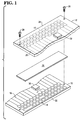
- printed circuit boards 10 and 12 are to be connected together into an assembly 30.
- Printed circuit board 10 is preferably a mother board, while printed circuit board 12 may be a peripheral adapter card, a memory expansion card, or a daughter board.
- Printed circuit boards 10 and 12 include connection pads 14 and 16, which are connected to the many electronic components of printed circuit boards 10 and 12 through traces 18 and 20.
- each connection pad on printed circuit board 10 preferably has a corresponding connection pad on printed circuit board 12.
- power and ground connection pads may have different geometries on each board. For example, a single large power connection pad on one printed circuit board may connect to many smaller power connection pads on the other printed circuit board.
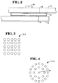
- Connection pads 14 and 16 are arranged in two-dimensional arrays, which may have a rectangular shape (Fig. 1), a square shape (Fig. 3), or an ovular or circular shape (Fig. 4), for example. Connection pads 14 and 16 are preferably flush with the connecting surfaces of printed circuit boards 10 and 12 as shown in Fig. 1, but they may be raised slightly higher than the connecting surfaces as shown in Fig. 2.
- the rows of Figs. 1 and 2 are arranged parallel and adjacent to the connecting sides 22 and 24 of printed circuit boards 10 and 12, however, connection pads 14 could be anywhere within the surface area of printed circuit board 10.
- a mother-daughter board combination shown in Fig. 5 requires connection pads 14 to be located away from sides 22.
- connection pads 14 and 16 are a thin sheet or mat 26 of anisotropically conductive material.
- This material is commercially available.
- a suitable material is ECPI (elastomeric conductive polymer interconnect) material, available from AT&T Corp. The boards are then pressed together and held in place by fasteners 28.
- Connection pads 14 and 16 may be arranged to meet specific space requirements.
- connection pads 14 and 16 are shown as square in shape, but they may also be circular (Fig. 3) or any other shape to further minimize space requirements.
- the electrical characteristics are also better and provide significantly higher maximum data transfer rates (bits per second) than ordinary connection schemes.
- the apparatus of the present invention is suitable for high-frequency applications up to 2 GHz, largely due to the shorter distance between the signal connectors on the respective circuit boards and the large contact areas, compared to traditional pin connectors.
Landscapes
- Engineering & Computer Science (AREA)
- Manufacturing & Machinery (AREA)
- Microelectronics & Electronic Packaging (AREA)
- Metallurgy (AREA)
- Combinations Of Printed Boards (AREA)
- Electric Connection Of Electric Components To Printed Circuits (AREA)
Applications Claiming Priority (2)
| Application Number | Priority Date | Filing Date | Title |
|---|---|---|---|
| US347023 | 1991-08-19 | ||
| US34702394A | 1994-11-30 | 1994-11-30 |
Publications (2)
| Publication Number | Publication Date |
|---|---|
| EP0715489A2 true EP0715489A2 (fr) | 1996-06-05 |
| EP0715489A3 EP0715489A3 (fr) | 1997-02-19 |
Family
ID=23362009
Family Applications (1)
| Application Number | Title | Priority Date | Filing Date |
|---|---|---|---|
| EP95308025A Withdrawn EP0715489A3 (fr) | 1994-11-30 | 1995-11-09 | Assemblage de panneaux à circuit imprimé |
Country Status (3)
| Country | Link |
|---|---|
| US (1) | US5627730A (fr) |
| EP (1) | EP0715489A3 (fr) |
| JP (1) | JPH08228074A (fr) |
Cited By (2)
| Publication number | Priority date | Publication date | Assignee | Title |
|---|---|---|---|---|
| EP1143577A3 (fr) * | 2000-04-05 | 2002-08-21 | Kitagawa Industries Co., Ltd. | Elément conducteur et son procédé de fabrication |
| WO2004002203A1 (fr) * | 2002-06-25 | 2003-12-31 | Nec Corporation | Dispositifs de cartes de circuits imprimes et procede de connexion entre cartes |
Families Citing this family (10)
| Publication number | Priority date | Publication date | Assignee | Title |
|---|---|---|---|---|
| US5856636A (en) * | 1997-03-03 | 1999-01-05 | Sanso; David W. | Electronic circuit prototype wiring board with visually distinctive contact pads |
| JPH10307641A (ja) * | 1997-05-07 | 1998-11-17 | Toshiba Corp | 電子機器 |
| US6412023B1 (en) * | 1998-05-21 | 2002-06-25 | Sony Corporation | System for communicating status via first signal line in a period of time in which control signal via second line is not transmitted |
| US6164979A (en) * | 1999-03-12 | 2000-12-26 | Motorola, Inc. | System for providing a removable high density electrical interconnect for flexible circuits |
| JP2001031929A (ja) * | 1999-07-21 | 2001-02-06 | Sony Chem Corp | 接続構造体 |
| JP2003249591A (ja) * | 2002-02-26 | 2003-09-05 | Nec Electronics Corp | エリアio型半導体装置の配線基板の設計方法 |
| JP4584144B2 (ja) * | 2003-01-22 | 2010-11-17 | 日本電気株式会社 | 回路基板装置及び配線基板間接続方法 |
| WO2010086956A1 (fr) * | 2009-01-27 | 2010-08-05 | エヌワイ工業株式会社 | Structure de connexion de substrat flexible et d'élément opposé |
| KR101996653B1 (ko) * | 2012-10-30 | 2019-07-05 | 삼성디스플레이 주식회사 | 평판표시장치 |
| CN106911023A (zh) * | 2017-03-28 | 2017-06-30 | 上海航天科工电器研究院有限公司 | 一种平行板间高传输速率的电连接器 |
Family Cites Families (24)
| Publication number | Priority date | Publication date | Assignee | Title |
|---|---|---|---|---|
| US4209481A (en) * | 1976-04-19 | 1980-06-24 | Toray Industries, Inc. | Process for producing an anisotropically electroconductive sheet |
| US4249302A (en) * | 1978-12-28 | 1981-02-10 | Ncr Corporation | Multilayer printed circuit board |
| US4423435A (en) * | 1980-10-27 | 1983-12-27 | Texas Instruments Incorporated | Assembly of an electronic device on an insulative substrate |
| US4729809A (en) * | 1985-03-14 | 1988-03-08 | Amp Incorporated | Anisotropically conductive adhesive composition |
| US4770641A (en) * | 1986-03-31 | 1988-09-13 | Amp Incorporated | Conductive gel interconnection apparatus |
| US4737112A (en) * | 1986-09-05 | 1988-04-12 | American Telephone And Telegraph Company, At&T Bell Laboratories | Anisotropically conductive composite medium |
| US4811081A (en) * | 1987-03-23 | 1989-03-07 | Motorola, Inc. | Semiconductor die bonding with conductive adhesive |
| JPS63249393A (ja) * | 1987-04-03 | 1988-10-17 | シャープ株式会社 | 電子部品の接続方法 |
| JPH01206575A (ja) * | 1988-02-15 | 1989-08-18 | Shin Etsu Polymer Co Ltd | 接着性熱融着形コネクタ |
| JPH0291360U (fr) * | 1988-12-29 | 1990-07-19 | ||
| SE469453B (sv) * | 1989-10-27 | 1993-07-05 | Ericsson Telefon Ab L M | Optisk kopplingsanordning |
| JP3154713B2 (ja) * | 1990-03-16 | 2001-04-09 | 株式会社リコー | 異方性導電膜およびその製造方法 |
| JP2598152B2 (ja) * | 1990-04-28 | 1997-04-09 | シャープ株式会社 | タッチパネル |
| US5174766A (en) * | 1990-05-11 | 1992-12-29 | Canon Kabushiki Kaisha | Electrical connecting member and electric circuit member |
| US5174763A (en) * | 1990-06-11 | 1992-12-29 | Itt Corporation | Contact assembly |
| US5140405A (en) * | 1990-08-30 | 1992-08-18 | Micron Technology, Inc. | Semiconductor assembly utilizing elastomeric single axis conductive interconnect |
| US5136365A (en) * | 1990-09-27 | 1992-08-04 | Motorola, Inc. | Anisotropic conductive adhesive and encapsulant material |
| JPH07123179B2 (ja) * | 1990-10-05 | 1995-12-25 | 信越ポリマー株式会社 | 異方導電接着剤による回路基板の接続構造 |
| WO1992021167A1 (fr) * | 1991-05-20 | 1992-11-26 | Elastomeric Technologies, Inc. | Connecteur electronique a elements conducteurs en elastomere |
| US5155302A (en) * | 1991-06-24 | 1992-10-13 | At&T Bell Laboratories | Electronic device interconnection techniques |
| JP2846751B2 (ja) * | 1991-07-03 | 1999-01-13 | ローム株式会社 | 回路基板に対するフレキシブルケーブルの接続装置 |
| US5165984A (en) * | 1991-07-30 | 1992-11-24 | At&T Bell Laboratories | Stepped multilayer interconnection apparatus and method of making the same |
| US5206585A (en) * | 1991-12-02 | 1993-04-27 | At&T Bell Laboratories | Methods for testing integrated circuit devices |
| US5417577A (en) * | 1992-09-23 | 1995-05-23 | At&T Corp. | Interconnection method and apparatus |
-
1995
- 1995-11-09 EP EP95308025A patent/EP0715489A3/fr not_active Withdrawn
- 1995-11-30 JP JP7334372A patent/JPH08228074A/ja active Pending
-
1996
- 1996-02-26 US US08/606,663 patent/US5627730A/en not_active Expired - Lifetime
Non-Patent Citations (1)
| Title |
|---|
| None |
Cited By (3)
| Publication number | Priority date | Publication date | Assignee | Title |
|---|---|---|---|---|
| EP1143577A3 (fr) * | 2000-04-05 | 2002-08-21 | Kitagawa Industries Co., Ltd. | Elément conducteur et son procédé de fabrication |
| WO2004002203A1 (fr) * | 2002-06-25 | 2003-12-31 | Nec Corporation | Dispositifs de cartes de circuits imprimes et procede de connexion entre cartes |
| US7501584B2 (en) | 2002-06-25 | 2009-03-10 | Nec Corporation | Circuit board device and method for board-to-board connection |
Also Published As
| Publication number | Publication date |
|---|---|
| EP0715489A3 (fr) | 1997-02-19 |
| JPH08228074A (ja) | 1996-09-03 |
| US5627730A (en) | 1997-05-06 |
Similar Documents
| Publication | Publication Date | Title |
|---|---|---|
| US4401351A (en) | Expandable card cage | |
| US5335146A (en) | High density packaging for device requiring large numbers of unique signals utilizing orthogonal plugging and zero insertion force connetors | |
| US7103753B2 (en) | Backplane system having high-density electrical connectors | |
| US5908333A (en) | Connector with integral transmission line bus | |
| US6491526B2 (en) | Riser card assembly and method for its installation | |
| US5266833A (en) | Integrated circuit bus structure | |
| EP0715489A2 (fr) | Assemblage de panneaux à circuit imprimé | |
| EP1134669A1 (fr) | Structure de bus incrémentielle pour équipement électronique modulaire | |
| EP0886219A3 (fr) | Système de server d'ordinateur avec carte d'adaptation redondante sans câble sur une carte d'entrée/sortie | |
| US6381140B1 (en) | Memory module | |
| US6122161A (en) | Circuit board assembly | |
| US6504725B1 (en) | Topology for PCI bus riser card system | |
| US6261106B1 (en) | IC card connector apparatus | |
| EP0815709A1 (fr) | Ensemble carte mere possedant une prise unique pouvant accepter un ou plusieurs boitiers de circuits integres | |
| JP4152954B2 (ja) | アドイン・カードをバックプレーンに接続するための装置、システム、方法 | |
| JP2001111262A (ja) | ラック装着用基板及びラック装着用基板の実装方法 | |
| US12550281B2 (en) | Riser card for a vertical mounting of an expansion card | |
| TWI403029B (zh) | Pci express連接器、系統及其方法 | |
| EP0718931B1 (fr) | Face arrière cylindrique multi-couche | |
| CN107426919B (zh) | 存储设备 | |
| US20250210922A1 (en) | Dual-sided connector for connecting a signal cable to a floating hardware component and associated method | |
| KR20010042599A (ko) | 고속 버스 접속 시스템 | |
| RU227574U1 (ru) | Плата объединительная накопителей данных М.2 (Матуа) | |
| CN220627047U (zh) | 硬盘系统 | |
| JPH0723990Y2 (ja) | 入出力処理装置のプリント板実装構造 |
Legal Events
| Date | Code | Title | Description |
|---|---|---|---|
| PUAI | Public reference made under article 153(3) epc to a published international application that has entered the european phase |
Free format text: ORIGINAL CODE: 0009012 |
|
| AK | Designated contracting states |
Kind code of ref document: A2 Designated state(s): DE FR GB |
|
| PUAL | Search report despatched |
Free format text: ORIGINAL CODE: 0009013 |
|
| AK | Designated contracting states |
Kind code of ref document: A3 Designated state(s): DE FR GB |
|
| 17P | Request for examination filed |
Effective date: 19970819 |
|
| 17Q | First examination report despatched |
Effective date: 19971216 |
|
| STAA | Information on the status of an ep patent application or granted ep patent |
Free format text: STATUS: THE APPLICATION IS DEEMED TO BE WITHDRAWN |
|
| 18D | Application deemed to be withdrawn |
Effective date: 19980427 |