EP0716524A1 - Détecteur de phase - Google Patents
Détecteur de phase Download PDFInfo
- Publication number
- EP0716524A1 EP0716524A1 EP95118983A EP95118983A EP0716524A1 EP 0716524 A1 EP0716524 A1 EP 0716524A1 EP 95118983 A EP95118983 A EP 95118983A EP 95118983 A EP95118983 A EP 95118983A EP 0716524 A1 EP0716524 A1 EP 0716524A1
- Authority
- EP
- European Patent Office
- Prior art keywords
- data
- memory
- signal
- phase detector
- detector circuit
- Prior art date
- Legal status (The legal status is an assumption and is not a legal conclusion. Google has not performed a legal analysis and makes no representation as to the accuracy of the status listed.)
- Granted
Links
Images


Classifications
-
- H—ELECTRICITY
- H03—ELECTRONIC CIRCUITRY
- H03K—PULSE TECHNIQUE
- H03K5/00—Manipulating of pulses not covered by one of the other main groups of this subclass
- H03K5/22—Circuits having more than one input and one output for comparing pulses or pulse trains with each other according to input signal characteristics, e.g. slope, integral
- H03K5/26—Circuits having more than one input and one output for comparing pulses or pulse trains with each other according to input signal characteristics, e.g. slope, integral the characteristic being duration, interval, position, frequency, or sequence
-
- G—PHYSICS
- G01—MEASURING; TESTING
- G01R—MEASURING ELECTRIC VARIABLES; MEASURING MAGNETIC VARIABLES
- G01R25/00—Arrangements for measuring phase angle between a voltage and a current or between voltages or currents
- G01R25/08—Arrangements for measuring phase angle between a voltage and a current or between voltages or currents by counting of standard pulses
-
- H—ELECTRICITY
- H03—ELECTRONIC CIRCUITRY
- H03D—DEMODULATION OR TRANSFERENCE OF MODULATION FROM ONE CARRIER TO ANOTHER
- H03D13/00—Circuits for comparing the phase or frequency of two mutually-independent oscillations
-
- H—ELECTRICITY
- H04—ELECTRIC COMMUNICATION TECHNIQUE
- H04L—TRANSMISSION OF DIGITAL INFORMATION, e.g. TELEGRAPHIC COMMUNICATION
- H04L7/00—Arrangements for synchronising receiver with transmitter
- H04L7/02—Speed or phase control by the received code signals, the signals containing no special synchronisation information
- H04L7/033—Speed or phase control by the received code signals, the signals containing no special synchronisation information using the transitions of the received signal to control the phase of the synchronising-signal-generating means, e.g. using a phase-locked loop
Definitions
- the invention relates to a phase detector for determining the phase difference between a digitized data signal and the clock signal of a receiving device.
- a phase signal is obtained as a control criterion, which after comparison with a reference signal is used to adjust the frequency of a clock generator or adjusts its phase.
- phase detector is in IEEE, Journal of Lightwave Technology, VOL. LT-3, No. 6,. Pages 1312 to 1314.
- This phase detector consists of two D flip-flops controlled by an internal clock and two EXCLUSIVE-OR gates, the inputs of an EXCLUSIVE-OR gate being connected to the input and output of a flip-flop. In this way, a phase signal and a reference signal are generated, which are subtracted from one another and - smoothed by a filter - control an oscillator which generates the clock signal.
- the flip-flops are each made up of two clock-state-controlled memory stages for runtime reasons. From each of these flip-flops, the second memory stage is driven with a clock signal inverted to the clock signal of the first memory stage or internally configured such that it responds to the inverted state of the clock signal.
- the maximum data rate that can be processed is essentially determined by the runtime of the storage levels.
- the outputs of the flip-flops are loaded unequally, which can lead to a temperature response of the circuit.
- the object of the invention is to provide a phase detector circuit suitable for extremely high data rates.
- a great advantage results from the use of two parallel data paths implemented by shift registers and a clock signal whose frequency corresponds to half the data rate.
- One bit of the original data signal is alternately taken into the data paths and shifted to the outputs of the shift register at half the original data rate.
- the data bits present in parallel can continue to be processed in parallel; Likewise, a sampled signal can be restored at the original data rate using a multiplexer.
- a particular advantage is - in addition to halving the data rate in the phase detector branches - that the first memory stage of each of these data paths is switched transparently with an 'active' clock signal and acts as a delay element in this state.
- EXCLUSIVE-OR gate can be switched on. These ensure equal and low loads at the data outputs and generate steep edges by amplifying the output data signals, so that an exact phase signal and an exact reference signal are obtained.
- the load on the individual memory stages of the phase detector circuit can be built up completely symmetrically by switching on inputs of additional amplifier elements.
- a second EXCLUSIVE-OR gate can also be switched on to generate a second reference voltage, which is combined with the previous reference voltage. This results in a less fluctuating resulting reference value.
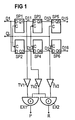
- the phase detector circuit shown in FIG. 1 contains two data paths, each with three memory stages connected in series.
- a data signal D1 is fed to the data input D of the first memory stage SP1 and SP2 of each data path.
- the memory stages of each data path are alternately at their clock inputs C with a non-inverted and an inverted clock signal CL or CL ⁇ driven, whose clock frequency corresponds to half the data rate.
- the first, second and third flip-flops SP2, SP4 and SP6 des second data path is driven with a clock signal inverted to the clock signal of the first, second or third memory stage SP1, SP3 and SP5 of the first data path. It is of course also possible to use memory stages which react to inverted clock signals, as symbolically shown in FIG.
- the data outputs Q1 and Q2 of the first memory stages SP1 and SP2 are routed via amplifier circuits (drivers) TV1 and TV2 to inputs of a first EXCLUSIVE-OR-GATTERS (or EXCLUSIVE-NOR-GATTERS) EX1.
- This gate generates the phase signal P.
- a reference signal R is generated by a second EXCLUSIVE-OR gate (or EXCLUSIVE-NOR-GATTERS) EX2, the first input of which is also connected to the output of the second amplifier stage TV2 and the second input of which is via a third Amplifier circuit TV3 is connected to the data output Q3 of a third memory stage SP3, which is connected downstream of the first memory stage SP1.
- the reference signal can also be obtained at a later time by comparing the sampled data signal.
- the third memory stage SP6 of the second data path ensures the same load on the flip-flop outputs Q2 and Q4 and decouples the actual phase detector circuit from the subsequent components.
- the memory stages SP3 and SP5 of the first data path serve to compensate for the data transit times in the two data paths.
- the output data signals D15 and D16 are output at the data outputs Q5, Q6 of the last memory stages SP5, SP6 of the data paths.
- FIG. 2 A particularly advantageous variant is shown in FIG. 2, in which a second reference signal R * is also generated, which is already shown in the time diagrams in FIGS. 2 and 3.
- a third EXCLUSIVE-OR-GATE EX3 is connected to the corresponding data outputs Q1 and Q3 of the first data path via a further amplifier circuit TV4.
- R and R * ensures a more frequent change between the two logic states of a resulting reference signal, which are compared with the phase signal.
- R 2P - (R + R *) ; this can be modified by coefficients.
- the phase detector circuits compare the received data signal with a data signal sampled with the clock signal CL of the receiving device (i.e. they measure the phase difference between the received data signal and the clock signal). The result is generally compared with a reference signal which is formed from bits of the data signal which have already been sampled and which - as a mean value - is proportional to the phase signal.
- the bits of the data signal are alternated with the log state. 1 of the halved clock signal CL obtained by division from an original clock signal CL0 in the upper data path to the output Q2 of the memory stage SP2 with the state of the log. 1 of the clock signal and to the output Q1 of the memory stage SP1 of the lower one Data path switched through with the state of log.0 of the clock signal and stored with its negative or positive edge.
- the memory stage SP1 is switched to be transparent in the case of a clock signal representing the logic “1” and thus the data signal D1 is switched through to its output Q1 as data signal D11, the state of the data signal preceding this edge of the clock signal initially remains stored as data signal D12 in the memory stage SP2.
- the first EXCLUSIVE-OR-GATTER EX1 compares a data signal D11 or D12 that is switched through with a sampled signal D12 or D11 and thus forms the phase signal P. With the next edge of the clock signal CL, the described states are reversed.
- Each first storage stage thus works alternately as a delay element and as a storage stage.
- the data signals D11 and D12 switched through by the first storage stages are taken over by the downstream storage stages SP3 and SP4 and temporarily stored as data signals D13 and D14.
- the individual bits of the data signal are labeled B1, B2, ....
- the reference signal R can take place, for example, in each data path (shift register) by comparing clocked data bits at different memory stage outputs.
- FIG. 1 also shows a particularly advantageous and cost-saving solution for this, in which the reference signal is formed in each case by the output signals D12 and D14 of the first and second flip-flops of a data path. The influence of the different position of the edges of the data signal is eliminated when the reference signal is formed.
- the amplifier stages TV1 to TV4 not only serve to keep the loads on the memory stage outputs low, they also serve to amplify the signals.
- the first storage stages cannot yet completely eliminate fluctuations in the amplitude of the input signal. However, by comparing signals with different amplitudes, errors occur that act as errors of the phase signal and the reference signal.
- the output signals are amplified and limited by the amplifier stages, so that signals with the same amplitudes and distributed edges are always compared.
Landscapes
- Physics & Mathematics (AREA)
- Engineering & Computer Science (AREA)
- Nonlinear Science (AREA)
- Computer Networks & Wireless Communication (AREA)
- Signal Processing (AREA)
- General Physics & Mathematics (AREA)
- Power Engineering (AREA)
- Manipulation Of Pulses (AREA)
- Stabilization Of Oscillater, Synchronisation, Frequency Synthesizers (AREA)
- Synchronisation In Digital Transmission Systems (AREA)
Applications Claiming Priority (2)
| Application Number | Priority Date | Filing Date | Title |
|---|---|---|---|
| DE4443417 | 1994-12-06 | ||
| DE4443417A DE4443417C1 (de) | 1994-12-06 | 1994-12-06 | Phasendetektorschaltung |
Publications (2)
| Publication Number | Publication Date |
|---|---|
| EP0716524A1 true EP0716524A1 (fr) | 1996-06-12 |
| EP0716524B1 EP0716524B1 (fr) | 2001-02-28 |
Family
ID=6535064
Family Applications (1)
| Application Number | Title | Priority Date | Filing Date |
|---|---|---|---|
| EP95118983A Expired - Lifetime EP0716524B1 (fr) | 1994-12-06 | 1995-12-01 | Détecteur de phase |
Country Status (2)
| Country | Link |
|---|---|
| EP (1) | EP0716524B1 (fr) |
| DE (2) | DE4443417C1 (fr) |
Cited By (1)
| Publication number | Priority date | Publication date | Assignee | Title |
|---|---|---|---|---|
| DE19717586C1 (de) * | 1997-04-25 | 1998-08-27 | Siemens Ag | Takt- und Datenregenerator für hohe Datenraten |
Families Citing this family (3)
| Publication number | Priority date | Publication date | Assignee | Title |
|---|---|---|---|---|
| DE19948690C2 (de) * | 1999-09-30 | 2002-05-23 | Infineon Technologies Ag | Phasendetektor |
| DE10215087B4 (de) * | 2002-04-05 | 2004-08-19 | Infineon Technologies Ag | Verfahren und Vorrichtung zur Phasendetektion |
| DE10216281B4 (de) * | 2002-04-12 | 2007-04-12 | Noé, Reinhold, Prof. Dr.-Ing. | Anordnung und Verfahren für eine Dispersionsdetektion |
Citations (3)
| Publication number | Priority date | Publication date | Assignee | Title |
|---|---|---|---|---|
| EP0054322A1 (fr) * | 1980-12-12 | 1982-06-23 | Philips Electronics Uk Limited | Détecteur sensible à la phase |
| GB2242085A (en) * | 1990-02-14 | 1991-09-18 | Daiichi Denshi Kogyo | Timing adjustment circuit for serial data |
| US5301196A (en) * | 1992-03-16 | 1994-04-05 | International Business Machines Corporation | Half-speed clock recovery and demultiplexer circuit |
-
1994
- 1994-12-06 DE DE4443417A patent/DE4443417C1/de not_active Expired - Fee Related
-
1995
- 1995-12-01 EP EP95118983A patent/EP0716524B1/fr not_active Expired - Lifetime
- 1995-12-01 DE DE59509059T patent/DE59509059D1/de not_active Expired - Fee Related
Patent Citations (3)
| Publication number | Priority date | Publication date | Assignee | Title |
|---|---|---|---|---|
| EP0054322A1 (fr) * | 1980-12-12 | 1982-06-23 | Philips Electronics Uk Limited | Détecteur sensible à la phase |
| GB2242085A (en) * | 1990-02-14 | 1991-09-18 | Daiichi Denshi Kogyo | Timing adjustment circuit for serial data |
| US5301196A (en) * | 1992-03-16 | 1994-04-05 | International Business Machines Corporation | Half-speed clock recovery and demultiplexer circuit |
Cited By (1)
| Publication number | Priority date | Publication date | Assignee | Title |
|---|---|---|---|---|
| DE19717586C1 (de) * | 1997-04-25 | 1998-08-27 | Siemens Ag | Takt- und Datenregenerator für hohe Datenraten |
Also Published As
| Publication number | Publication date |
|---|---|
| EP0716524B1 (fr) | 2001-02-28 |
| DE59509059D1 (de) | 2001-04-05 |
| DE4443417C1 (de) | 1996-02-22 |
Similar Documents
| Publication | Publication Date | Title |
|---|---|---|
| DE69527931T2 (de) | Ausgangssteuerschaltung für eine Übertragungsleistungsschaltung | |
| DE69410410T2 (de) | Taktsignalgenerator für eine Vielzahl nicht überlappender Taktsignale | |
| EP0447593B1 (fr) | Circuit CAG utilisant la technologie MOS | |
| DE2715806A1 (de) | Schnelle korrelationsanordnung und damit ausgeruestetes signalverarbeitungssystem | |
| EP0491422A1 (fr) | Dispositif de conversion du taux d'échantillonage d'un signal numérique | |
| DE2015812A1 (de) | Hochfrequenz Leistungsverstärker | |
| DE1219966B (de) | Vorrichtung zur Ableitung einer Bezugsphase zur Demodulation von phasenmodulierten Signalen bestimmter Frequenz | |
| DE2446287B2 (de) | Kernresonanzspektrometer | |
| DE2711292A1 (de) | Verzoegerungsleitung | |
| EP0716524A1 (fr) | Détecteur de phase | |
| DE10130123A1 (de) | Verzögerungsregelkreis zur Erzeugung komplementärer Taktsignale | |
| EP0099142A2 (fr) | Procédé et dispositif de démodulation d'un signal d'entrée modulé en fréquence | |
| DE69018497T2 (de) | Digitales Filter. | |
| DE69931512T2 (de) | Phasendifferenzvergrösserer | |
| DE1591194B1 (de) | Diversity-Empfangssystem | |
| DE3751088T2 (de) | Signalverarbeitungseinrichtung. | |
| DE102006002735B3 (de) | Vorrichtung zur Korrektur des Tastverhältnisses in einem Taktsignal | |
| EP0463206B1 (fr) | Procédé pour mesurer des petites différences de phase et circuit pour appliquer ce procédé | |
| EP1099192B1 (fr) | Circuit semi-conducteur integre a horloge et son mode de fonctionnement | |
| DE602004008857T2 (de) | Leistungsverstärkungsschaltung | |
| DE3822857C1 (en) | Method and circuit arrangement for producing a phase-shifted clock signal | |
| EP0716523B1 (fr) | Détecteur de phase | |
| DE69411346T2 (de) | Schaltung zur Anzeige der Phasenverhältnisse zwischen mehreren Signalen mit gleicher Frequenz und ihre Anwendung in einer Schaltung zur Korrektur der Phasen zwischen diesen Signalen | |
| DE10302234A1 (de) | Flexibler Dezimator | |
| DE1950924A1 (de) | Decodierschaltung fuer phasenmodulierte Signale |
Legal Events
| Date | Code | Title | Description |
|---|---|---|---|
| PUAI | Public reference made under article 153(3) epc to a published international application that has entered the european phase |
Free format text: ORIGINAL CODE: 0009012 |
|
| AK | Designated contracting states |
Kind code of ref document: A1 Designated state(s): DE FR GB IT |
|
| 17P | Request for examination filed |
Effective date: 19960904 |
|
| 17Q | First examination report despatched |
Effective date: 19990906 |
|
| GRAG | Despatch of communication of intention to grant |
Free format text: ORIGINAL CODE: EPIDOS AGRA |
|
| GRAG | Despatch of communication of intention to grant |
Free format text: ORIGINAL CODE: EPIDOS AGRA |
|
| GRAH | Despatch of communication of intention to grant a patent |
Free format text: ORIGINAL CODE: EPIDOS IGRA |
|
| GRAH | Despatch of communication of intention to grant a patent |
Free format text: ORIGINAL CODE: EPIDOS IGRA |
|
| GRAA | (expected) grant |
Free format text: ORIGINAL CODE: 0009210 |
|
| AK | Designated contracting states |
Kind code of ref document: B1 Designated state(s): DE FR GB IT |
|
| REF | Corresponds to: |
Ref document number: 59509059 Country of ref document: DE Date of ref document: 20010405 |
|
| ET | Fr: translation filed | ||
| ITF | It: translation for a ep patent filed | ||
| GBT | Gb: translation of ep patent filed (gb section 77(6)(a)/1977) |
Effective date: 20010516 |
|
| REG | Reference to a national code |
Ref country code: GB Ref legal event code: IF02 |
|
| PLBE | No opposition filed within time limit |
Free format text: ORIGINAL CODE: 0009261 |
|
| STAA | Information on the status of an ep patent application or granted ep patent |
Free format text: STATUS: NO OPPOSITION FILED WITHIN TIME LIMIT |
|
| 26N | No opposition filed | ||
| PGFP | Annual fee paid to national office [announced via postgrant information from national office to epo] |
Ref country code: DE Payment date: 20050217 Year of fee payment: 10 |
|
| PGFP | Annual fee paid to national office [announced via postgrant information from national office to epo] |
Ref country code: GB Payment date: 20051208 Year of fee payment: 11 |
|
| PGFP | Annual fee paid to national office [announced via postgrant information from national office to epo] |
Ref country code: FR Payment date: 20051216 Year of fee payment: 11 |
|
| PG25 | Lapsed in a contracting state [announced via postgrant information from national office to epo] |
Ref country code: DE Free format text: LAPSE BECAUSE OF NON-PAYMENT OF DUE FEES Effective date: 20060701 |
|
| PGFP | Annual fee paid to national office [announced via postgrant information from national office to epo] |
Ref country code: IT Payment date: 20061231 Year of fee payment: 12 |
|
| GBPC | Gb: european patent ceased through non-payment of renewal fee |
Effective date: 20061201 |
|
| REG | Reference to a national code |
Ref country code: FR Ref legal event code: ST Effective date: 20070831 |
|
| PG25 | Lapsed in a contracting state [announced via postgrant information from national office to epo] |
Ref country code: GB Free format text: LAPSE BECAUSE OF NON-PAYMENT OF DUE FEES Effective date: 20061201 |
|
| PG25 | Lapsed in a contracting state [announced via postgrant information from national office to epo] |
Ref country code: FR Free format text: LAPSE BECAUSE OF NON-PAYMENT OF DUE FEES Effective date: 20070102 |
|
| PG25 | Lapsed in a contracting state [announced via postgrant information from national office to epo] |
Ref country code: IT Free format text: LAPSE BECAUSE OF NON-PAYMENT OF DUE FEES Effective date: 20071201 |