EP0716540A2 - Circuit de compensation du décalage de la composante continue pour la télévision pal-plus - Google Patents
Circuit de compensation du décalage de la composante continue pour la télévision pal-plus Download PDFInfo
- Publication number
- EP0716540A2 EP0716540A2 EP95119167A EP95119167A EP0716540A2 EP 0716540 A2 EP0716540 A2 EP 0716540A2 EP 95119167 A EP95119167 A EP 95119167A EP 95119167 A EP95119167 A EP 95119167A EP 0716540 A2 EP0716540 A2 EP 0716540A2
- Authority
- EP
- European Patent Office
- Prior art keywords
- signal
- helper
- output signal
- direct current
- demodulating
- Prior art date
- Legal status (The legal status is an assumption and is not a legal conclusion. Google has not performed a legal analysis and makes no representation as to the accuracy of the status listed.)
- Granted
Links
- 230000003111 delayed effect Effects 0.000 claims abstract description 7
- 238000001914 filtration Methods 0.000 claims abstract description 3
- 238000005070 sampling Methods 0.000 claims description 11
- 230000001360 synchronised effect Effects 0.000 claims description 5
- 238000010586 diagram Methods 0.000 description 4
- 230000007423 decrease Effects 0.000 description 2
- 230000003247 decreasing effect Effects 0.000 description 2
- 230000006866 deterioration Effects 0.000 description 1
- 230000000694 effects Effects 0.000 description 1
Images

Classifications
-
- H—ELECTRICITY
- H04—ELECTRIC COMMUNICATION TECHNIQUE
- H04N—PICTORIAL COMMUNICATION, e.g. TELEVISION
- H04N11/00—Colour television systems
- H04N11/06—Transmission systems characterised by the manner in which the individual colour picture signal components are combined
- H04N11/12—Transmission systems characterised by the manner in which the individual colour picture signal components are combined using simultaneous signals only
- H04N11/14—Transmission systems characterised by the manner in which the individual colour picture signal components are combined using simultaneous signals only in which one signal, modulated in phase and amplitude, conveys colour information and a second signal conveys brightness information, e.g. NTSC-system
- H04N11/16—Transmission systems characterised by the manner in which the individual colour picture signal components are combined using simultaneous signals only in which one signal, modulated in phase and amplitude, conveys colour information and a second signal conveys brightness information, e.g. NTSC-system the chrominance signal alternating in phase, e.g. PAL-system
-
- H—ELECTRICITY
- H04—ELECTRIC COMMUNICATION TECHNIQUE
- H04N—PICTORIAL COMMUNICATION, e.g. TELEVISION
- H04N5/00—Details of television systems
- H04N5/14—Picture signal circuitry for video frequency region
- H04N5/16—Circuitry for reinsertion of DC and slowly varying components of signal; Circuitry for preservation of black or white level
-
- H—ELECTRICITY
- H04—ELECTRIC COMMUNICATION TECHNIQUE
- H04N—PICTORIAL COMMUNICATION, e.g. TELEVISION
- H04N11/00—Colour television systems
- H04N11/06—Transmission systems characterised by the manner in which the individual colour picture signal components are combined
- H04N11/12—Transmission systems characterised by the manner in which the individual colour picture signal components are combined using simultaneous signals only
- H04N11/14—Transmission systems characterised by the manner in which the individual colour picture signal components are combined using simultaneous signals only in which one signal, modulated in phase and amplitude, conveys colour information and a second signal conveys brightness information, e.g. NTSC-system
- H04N11/16—Transmission systems characterised by the manner in which the individual colour picture signal components are combined using simultaneous signals only in which one signal, modulated in phase and amplitude, conveys colour information and a second signal conveys brightness information, e.g. NTSC-system the chrominance signal alternating in phase, e.g. PAL-system
- H04N11/167—Transmission systems characterised by the manner in which the individual colour picture signal components are combined using simultaneous signals only in which one signal, modulated in phase and amplitude, conveys colour information and a second signal conveys brightness information, e.g. NTSC-system the chrominance signal alternating in phase, e.g. PAL-system a resolution-increasing signal being multiplexed to the PAL-system signal, e.g. PAL-PLUS-system
-
- H—ELECTRICITY
- H04—ELECTRIC COMMUNICATION TECHNIQUE
- H04N—PICTORIAL COMMUNICATION, e.g. TELEVISION
- H04N9/00—Details of colour television systems
- H04N9/79—Processing of colour television signals in connection with recording
- H04N9/80—Transformation of the television signal for recording, e.g. modulation, frequency changing; Inverse transformation for playback
- H04N9/82—Transformation of the television signal for recording, e.g. modulation, frequency changing; Inverse transformation for playback the individual colour picture signal components being recorded simultaneously only
- H04N9/83—Transformation of the television signal for recording, e.g. modulation, frequency changing; Inverse transformation for playback the individual colour picture signal components being recorded simultaneously only the recorded chrominance signal occupying a frequency band under the frequency band of the recorded brightness signal
- H04N9/832—Transformation of the television signal for recording, e.g. modulation, frequency changing; Inverse transformation for playback the individual colour picture signal components being recorded simultaneously only the recorded chrominance signal occupying a frequency band under the frequency band of the recorded brightness signal using an increased bandwidth for the luminance or the chrominance signal
Definitions
- the present invention relates to a direct current offset compensation circuit for a PAL plus television, and in particular to an improved direct current offset compensation circuit for a PAL plus television capable of preventing a direct current distortion by compensating a direct current offset when demodulating the helper signal outputted from a PAL plus video cassette tape recorder (hereinafter called a "VCR").
- VCR video cassette tape recorder
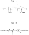
- Fig. 1 shows a helper signal demodulation circuit for a conventional PAL plus VCR, which includes a demodulating unit 10 for demodulating a helper signal H[t]COSWsct to a certain frequency and for outputting a low-pass component from the thusly demodulated signal, and an adder 20 for adding a direct current offset voltage "d" to the output signal of the demodulating unit 10.
- a demodulating unit 10 for demodulating a helper signal H[t]COSWsct to a certain frequency and for outputting a low-pass component from the thusly demodulated signal
- an adder 20 for adding a direct current offset voltage "d" to the output signal of the demodulating unit 10.
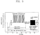
- Fig. 2 shows a helper signal remodulating circuit of a conventional PAL plus VCR, which includes an adder for decreasing the level of the helper signal d+H[t]+f reproduced by VCR by a level of the offset voltage "d", a multiplier 40 for remodulating the output signal of the adder to a certain frequency Fsc, and a band-pass filter 50 for outputting a certain band-pass component of the output signal of the multiplier.
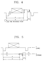
- a helper reference signal contained in a 23rd scanning line of a PAL plus signal includes a black level reference signal and a helper reference burst.
- the demodulating unit 10 and the adder 11 demodulate the helper signal H[t]COSWsct to a certain frequency, and the low-pass filter 12 outputs a certain low-pass component of the thusly demodulated signal.
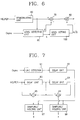
- the adder 20 adds a direct current offset voltage "d" to the output signal H(t) of the demodulating unit 10, and a certain signal d+H[t] having a wave form as shown in fig. 4 is outputted.
- a denotes an interval from a scanning line time reference point to a black level reference signal
- b denotes an interval from a scanning line time reference point to a helper reference burst signal
- c denotes a helper reference burst duration, in which a helper reference burst is demodulated
- e denotes a level difference decreased by a predetermined level.
- the adder 30 decreases the level of the reproduced helper signal d+H[t]+f by a level of the direct current offset voltage "d", and the multiplier 40 remodulates the signal to a certain frequency, and the band-pass filter 50 passes a certain band-pass component from the thusly remodulated signal, and outputs the remodulated helper signal H[t]+fCOSWsct .
- the helper signal is filtered by a band-pass filter by remodulating to a certain frequency Fsc, a luminance signal Y and a color signal C are divided as shown in Fig. 5.
- a direct current distortion "f" is contained in the black level reference signal as shown in Fig. 5 in the remodulated signal ⁇ (H[t]+f)COSWsct ⁇ . Therefore, since the direct current distortion "f" is a vertical high frequency in a PAL plus television, it becomes a factor which decreases the quality of picture resolution.
- a direct current offset compensation circuit for a PAL plus television which includes a demodulating unit for demodulating a helper signal to a certain frequency and for low-pass-filtering the signal; a level detecting unit for delaying an output signal of the demodulating unit at a certain scanning line and for detecting a direct current distortion and a peak value of a helper signal using an output signal of the demodulating unit and the thusly delayed signal; an adder for subtracting the direct current distortion detected by the level detecting unit from an output signal of the demodulating unit and for removing the direct current distortion from the thusly demodulated helper signal; a level setting unit for dividing a desired peak value of the helper signal by the peak value detected by the level detecting unit; and a multiplier for multiplying the output signal of the adder and the output signal of the level setting unit and for adjusting the peak value of the desired helper signal to a certain level.
- Fig. 1 is a block diagram of a helper signal demodulating unit for a conventional PAL VCR.
- Fig. 2 is a block diagram of a helper signal remodulating unit for a conventional PAL VCR.
- Fig. 3 is a wave form of a helper reference signal of a PAL plus signal of a conventional PAL LCR.
- Fig. 4 is a wave form of a demodulated helper signal of Fig. 1.
- Fig. 5 is a wave form of a remodulated helper signal of Fig. 2.
- Fig. 6 is a block diagram of a direct current offset compensation circuit of a PAL plus television according to the present invention.
- Fig. 7 is a block diagram of a level detecting unit of Fig. 6.
- Fig. 8 is a wave form of a demodulation of a helper signal according to the present invention.
- Fig. 6 shows a direct current offset compensation circuit for a PAL plus television according to the present invention, which includes a demodulating unit 60 for demodulating a helper signal, a level detecting unit 90 for detecting a direct current distortion "f" and a helper peak value "g" from the output signal of the demodulating unit 60 in accordance with a synchronous signal Csync of a combined video signal, an adder 70 for adding subtracting the output signal of the demodulating unit 60 by a direct current distortion "f" detected by the level detecting unit 90, a level setting unit 100 for dividing the final peak value "a” by a helper peak value "g” of the level detecting unit 90, and a multiplier 80 for multiplying the output signal "a/g" of the level setting unit 100 with the output signal of the adder 70 and for fixing the demodulated helper signal to have a desired output level.
- a demodulating unit 60 for demodulating a helper signal
- a level detecting unit 90 for detecting
- the level detecting unit 90 includes a line detector 91 for identifying a 23rd scanning line from a synchronous signal Csync of the combined video signal, a first delay unit 92 for delaying the output signal of the line detector 91 for a predetermined time, a second and third delay units 93 and 94 for delaying the demodulated helper signals for a predetermined time, respectively, a first adder 95 for subtracting the demodulated helper signal by the signal delayed by the second delay unit 93, a first sampling/holding unit 97 for sampling and holding the output signal of the first adder 95 in accordance with an output signal of the first delay unit 92, a second adder 96 for subtracting the output signal of the second delay unit 93 by the signal delayed by the third delay unit 94, and a second sampling/holding unit 98 for sampling and holding the output signal of the second adder 96 in accordance with an output signal of the first delay unit 92.
- Fig. 4 shows a demodulation wave form of a helper reference signal of a PAL plus VCR
- Fig. 5 shows a remodulation wave form.
- a reproducing signal is inputted to a PAL plus VCR, a luminance signal as shown in Fig. 8A and a color signal as shown in Fig. 8B are demodulated. That is, a helper reference signal as shown in Fig. 5 is redemodulated, and as a result a wave form as shown in Fig. 8B is obtained.
- the level detecting unit 90 checks the output signal of the demodulating unit 60 in accordance with a synchronous signal Csync of the combined video signal and computes a level "f" of a direct current distortion and a peak value "g" of a helper signal from the wave form as shown in Fig. 8B.
- the adder 70 subtracts the output signal of the demodulating unit 60 by a direct current distortion level "f" which is detected by the level detecting unit 90, and the direct current distortion is removed during a recording/reproducing.
- the level setting unit 100 adjusts a desired peak value.
- the desired peak value is as "a”
- a desired final peak value is divided by a computed peak value "g”
- the result value "a/g” is outputted to the multiplier 80.
- the multiplier 80 multiplies the output signal of the adder 70 by the output signal "a/g" of the level setting unit 100, the peak value of the demodulated helper signal is fixed as "a”. That is, the level of the helper signal is automatically adjusted in accordance with the output signal "a/g" of the level setting unit 100.
- the first delay unit 92 checks whether a certain time is lapsed from the time the 23rd scanning line is identified, and outputs a certain pulse when the certain time is lapsed.
- the first delay unit 92 has a certain time which is obtained by adding the intervals "h", "i” and "j" in the wave form as shown in Fig. 8B.
- the demodulated helper signal is outputted to the first adder 95 and the second adder 96, respectively, through the second and third delay units 93 and 94 in order.
- the second delay unit 93 has a certain delay time as much as the intervals "h" and "i” in the wave form of Fig. 8B
- the third delay unit 94 has a certain delay time as much as the intervals "j" in the wave form of Fig. 8B.
- the first delay unit 92 outputs a strobe pulse as shown in Fig. c to the first and second sampling/holding units 97 and 98 when a certain setting time is lapsed. Thereafter, the strobe pulse outputted from the first delay unit 92 is shifted from a low level to a high level, the first and second sampling/holding units 97 and 98 sample and hold the output signals "g" and "f" of the first and second adders 95 and 96. Since the helper reference signal is once inputted during one frame, the first and second sampling/holding units 97 and 98 holds the output signals "g" and "f” of the first and second adders 95 and 96 during one frame. These output signals "f” and “g” are inputted to the level setting unit 100, respectively, and are used as a signal for removing direct current distortions and automatically adjusting the peak level.
- the direct current offset compensation circuit for a PAL plus television is directed to preventing a direct current distortion before processing the demodulated helper signal, so that it is possible to prevent the deterioration of picture resolution and to automatically adjust the level of a helper signal to a desired level by computing the peak value of a helper signal.
Landscapes
- Engineering & Computer Science (AREA)
- Multimedia (AREA)
- Signal Processing (AREA)
- Processing Of Color Television Signals (AREA)
Applications Claiming Priority (2)
| Application Number | Priority Date | Filing Date | Title |
|---|---|---|---|
| KR3315694 | 1994-12-07 | ||
| KR1019940033156A KR100317351B1 (ko) | 1994-12-07 | 1994-12-07 | 팔프러스티브이의직류오프셋보상회로 |
Publications (3)
| Publication Number | Publication Date |
|---|---|
| EP0716540A2 true EP0716540A2 (fr) | 1996-06-12 |
| EP0716540A3 EP0716540A3 (fr) | 1996-12-18 |
| EP0716540B1 EP0716540B1 (fr) | 1999-09-22 |
Family
ID=19400610
Family Applications (1)
| Application Number | Title | Priority Date | Filing Date |
|---|---|---|---|
| EP95119167A Expired - Lifetime EP0716540B1 (fr) | 1994-12-07 | 1995-12-06 | Circuit de compensation du décalage de la composante continue pour la télévision pal-plus |
Country Status (3)
| Country | Link |
|---|---|
| EP (1) | EP0716540B1 (fr) |
| KR (1) | KR100317351B1 (fr) |
| DE (1) | DE69512359T2 (fr) |
Cited By (1)
| Publication number | Priority date | Publication date | Assignee | Title |
|---|---|---|---|---|
| EP0833524A3 (fr) * | 1996-09-27 | 1998-04-29 | SONY DEUTSCHLAND GmbH | Méthode et dispositif pour améliorer la qualité de reproduction d'un récepteur de télévision à écran large |
Family Cites Families (7)
| Publication number | Priority date | Publication date | Assignee | Title |
|---|---|---|---|---|
| GB8721565D0 (en) * | 1987-09-14 | 1987-10-21 | Rca Corp | Video signal processing system |
| JPH0810927B2 (ja) * | 1989-06-07 | 1996-01-31 | 株式会社東芝 | 多重信号伝送及び受信装置及びその方法 |
| DE4111979A1 (de) * | 1991-04-12 | 1992-10-15 | Thomson Brandt Gmbh | Vorrichtung zur bildsignal-aufzeichnung und/oder -wiedergabe |
| GB9126225D0 (en) * | 1991-12-10 | 1992-02-12 | British Broadcasting Corp | Enhanced composite television |
| JPH0822057B2 (ja) * | 1992-04-21 | 1996-03-04 | 松下電器産業株式会社 | テレビジョン信号処理方法および処理装置 |
| JPH06141293A (ja) * | 1992-10-27 | 1994-05-20 | Toshiba Corp | 直流オフセット除去テレビジョン信号処理回路 |
| JPH06292146A (ja) * | 1993-04-01 | 1994-10-18 | Matsushita Electric Ind Co Ltd | テレビジョン信号処理回路 |
-
1994
- 1994-12-07 KR KR1019940033156A patent/KR100317351B1/ko not_active Expired - Fee Related
-
1995
- 1995-12-06 DE DE69512359T patent/DE69512359T2/de not_active Expired - Fee Related
- 1995-12-06 EP EP95119167A patent/EP0716540B1/fr not_active Expired - Lifetime
Cited By (1)
| Publication number | Priority date | Publication date | Assignee | Title |
|---|---|---|---|---|
| EP0833524A3 (fr) * | 1996-09-27 | 1998-04-29 | SONY DEUTSCHLAND GmbH | Méthode et dispositif pour améliorer la qualité de reproduction d'un récepteur de télévision à écran large |
Also Published As
| Publication number | Publication date |
|---|---|
| EP0716540A3 (fr) | 1996-12-18 |
| KR960028598A (ko) | 1996-07-22 |
| DE69512359T2 (de) | 2000-02-24 |
| DE69512359D1 (de) | 1999-10-28 |
| KR100317351B1 (ko) | 2002-02-19 |
| EP0716540B1 (fr) | 1999-09-22 |
Similar Documents
| Publication | Publication Date | Title |
|---|---|---|
| US5294979A (en) | Estimation of noise using burst gate response to video signal | |
| EP0212674B1 (fr) | Circuit de suppression de bruit avec commande de gain | |
| US4514763A (en) | Sound signal and impulse noise detector for television receivers | |
| US5103297A (en) | Apparatus for carrying out y/c separation | |
| US4855812A (en) | Picture synthesizing apparatus with gain control system | |
| EP0289046B1 (fr) | Dispositif détecteur de fluctuations de base de temps pour un enregistreur à bande vidéo | |
| JPH0533599B2 (fr) | ||
| EP0618738B1 (fr) | Filtre en peigne capable de réduire le bruit et le phenomène d'intermodulation couleur | |
| CA1135834A (fr) | Compensateur de defauts pour la television en couleurs | |
| US5218438A (en) | Picture aperture correction circuit | |
| EP0716540A2 (fr) | Circuit de compensation du décalage de la composante continue pour la télévision pal-plus | |
| US4994923A (en) | Video signal recording and reproducing apparatus with signal processing circuit for improvement of picture quality | |
| US5323238A (en) | Image signal processing apparatus having improved storage control in accordance with an image signal level | |
| US5010416A (en) | Color video signal reproducing apparatus | |
| US5194964A (en) | Apparatus for processing color or black and white video signals | |
| US4571639A (en) | Dropout compensation circuit for a video reproducing system | |
| EP0462746B1 (fr) | Système de reproduction automatique d'un magnétoscope | |
| US5309226A (en) | Means for cancelling ghost signals in response to the reception of a non-standard television video signal | |
| JP3101393B2 (ja) | 映像信号処理装置 | |
| KR940004511B1 (ko) | 브이씨알의 재생 색신호 자동 보정 시스템 | |
| JP3101374B2 (ja) | 映像信号記録装置 | |
| JP3189526B2 (ja) | 映像色信号の雑音低減装置 | |
| JP2542301B2 (ja) | ビデオカセットレコ―ダ― | |
| JPS63178688A (ja) | 画像合成装置 | |
| JP3405025B2 (ja) | 色信号処理装置 |
Legal Events
| Date | Code | Title | Description |
|---|---|---|---|
| PUAI | Public reference made under article 153(3) epc to a published international application that has entered the european phase |
Free format text: ORIGINAL CODE: 0009012 |
|
| 17P | Request for examination filed |
Effective date: 19951206 |
|
| AK | Designated contracting states |
Kind code of ref document: A2 Designated state(s): DE |
|
| PUAL | Search report despatched |
Free format text: ORIGINAL CODE: 0009013 |
|
| AK | Designated contracting states |
Kind code of ref document: A3 Designated state(s): AT DE GB NL |
|
| GRAG | Despatch of communication of intention to grant |
Free format text: ORIGINAL CODE: EPIDOS AGRA |
|
| 17Q | First examination report despatched |
Effective date: 19981204 |
|
| GRAG | Despatch of communication of intention to grant |
Free format text: ORIGINAL CODE: EPIDOS AGRA |
|
| GRAH | Despatch of communication of intention to grant a patent |
Free format text: ORIGINAL CODE: EPIDOS IGRA |
|
| GRAH | Despatch of communication of intention to grant a patent |
Free format text: ORIGINAL CODE: EPIDOS IGRA |
|
| GRAA | (expected) grant |
Free format text: ORIGINAL CODE: 0009210 |
|
| AK | Designated contracting states |
Kind code of ref document: B1 Designated state(s): DE |
|
| REF | Corresponds to: |
Ref document number: 69512359 Country of ref document: DE Date of ref document: 19991028 |
|
| PLBE | No opposition filed within time limit |
Free format text: ORIGINAL CODE: 0009261 |
|
| STAA | Information on the status of an ep patent application or granted ep patent |
Free format text: STATUS: NO OPPOSITION FILED WITHIN TIME LIMIT |
|
| 26N | No opposition filed | ||
| PGFP | Annual fee paid to national office [announced via postgrant information from national office to epo] |
Ref country code: DE Payment date: 20081205 Year of fee payment: 14 |
|
| PG25 | Lapsed in a contracting state [announced via postgrant information from national office to epo] |
Ref country code: DE Free format text: LAPSE BECAUSE OF NON-PAYMENT OF DUE FEES Effective date: 20100701 |