EP0717363A2 - Anpassung eines Prozessorausbaus an ein Datenverarbeitungssystem - Google Patents
Anpassung eines Prozessorausbaus an ein Datenverarbeitungssystem Download PDFInfo
- Publication number
- EP0717363A2 EP0717363A2 EP95308555A EP95308555A EP0717363A2 EP 0717363 A2 EP0717363 A2 EP 0717363A2 EP 95308555 A EP95308555 A EP 95308555A EP 95308555 A EP95308555 A EP 95308555A EP 0717363 A2 EP0717363 A2 EP 0717363A2
- Authority
- EP
- European Patent Office
- Prior art keywords
- bus
- data
- bus master
- master
- processor
- Prior art date
- Legal status (The legal status is an assumption and is not a legal conclusion. Google has not performed a legal analysis and makes no representation as to the accuracy of the status listed.)
- Ceased
Links
Images


Classifications
-
- G—PHYSICS
- G06—COMPUTING OR CALCULATING; COUNTING
- G06F—ELECTRIC DIGITAL DATA PROCESSING
- G06F13/00—Interconnection of, or transfer of information or other signals between, memories, input/output devices or central processing units
- G06F13/38—Information transfer, e.g. on bus
- G06F13/40—Bus structure
-
- G—PHYSICS
- G06—COMPUTING OR CALCULATING; COUNTING
- G06F—ELECTRIC DIGITAL DATA PROCESSING
- G06F13/00—Interconnection of, or transfer of information or other signals between, memories, input/output devices or central processing units
- G06F13/38—Information transfer, e.g. on bus
- G06F13/40—Bus structure
- G06F13/4004—Coupling between buses
- G06F13/4009—Coupling between buses with data restructuring
- G06F13/4018—Coupling between buses with data restructuring with data-width conversion
-
- G—PHYSICS
- G06—COMPUTING OR CALCULATING; COUNTING
- G06F—ELECTRIC DIGITAL DATA PROCESSING
- G06F13/00—Interconnection of, or transfer of information or other signals between, memories, input/output devices or central processing units
- G06F13/14—Handling requests for interconnection or transfer
- G06F13/36—Handling requests for interconnection or transfer for access to common bus or bus system
Definitions
- the present invention relates in general to a method and system for data processing and in particular to a method and system for interfacing an upgrade processor to a data processing system having a disparate data path width. Still more particularly, the present invention relates to a method and system for interfacing a upgrade processor which processes transactions in m-byte packets of data to a data processing system which performs transactions utilizing n-byte packets of data.
- processors incorporating these advances in CPU technology provide greatly enhanced performance, they are not readily available for use as upgrade processors since they are often incompatible with existing computer systems.
- a second issue that must be addressed when interfacing a upgrade processor to a personal computer system is the scheme employed to arbitrate between the upgrade processor and bus master devices within the personal computer system for ownership of the system bus. Determining an efficient arbitration scheme is complicated by the fact that the upgrade processor may have a different arbitration protocol from that of the personal computer system if their architectures are dissimilar. For example, some processor architectures, such as the x86 architecture, can utilize a uni-directional (asynchronous) bus acquisition protocol, in which the requesting bus master expects to receive control of the system bus after asserting a request signal.
- bus masters utilize a bi-directional handshake bus acquisition protocol in which both a request signal by a second bus master and an acknowledge signal from the arbiter are required before the second bus master assumes control of the bus from the first bus master.
- Prior art systems do not support interfacing upgrade processors in personal computer systems which have incompatible arbitration protocols. Consequently, it would be desirable to provide a method and system for interfacing an upgrade processor to a personal computer system which utilizes a dissimilar arbitration protocol.
- a data processing system which includes a first processor having an m-byte data width, an n-byte data bus, where n is less than m, and a second processor electrically coupled to the bus which performs bus transactions utilizing n-byte packets of data.
- An adaptor is electrically coupled between the first processor and the bus which converts n-byte packets of data input from the bus to m-byte packets of data, and converts m-byte packets of data input from the first processor to n-byte packets of data, thereby enabling the first processor to transmit data to and receive data from the bus utilizing m-byte packets of data.
- a method and system are provided for arbitrating between two bus masters having disparate bus acquisition protocols.
- control of the bus is removed from the first bus master.
- control of the bus is granted to the second bus master.
- control of the bus is granted to the first bus master and a signal is transmitted from the arbitration control unit to the first bus master acknowledging the grant of control.
- Data processing system 10 comprises processing unit 12 , display device 14 , keyboard 16 , and mouse 18 .
- processing unit 12 comprises a personal computer designed to utilize a 32-bit 80x86 CISC processor, such as an IBM Personal System 2 (PS/2) Model 77.
- PS/2 IBM Personal System 2
- the performance of data processing system 10 is enhanced by replacing the CPU within processing unit 12 with an upgrade processor.
- processing unit 12 comprises processor 20 , adaptor 22 , x86 compatible devices 24 , additional devices 26 and hybrid bus 28 .
- the performance of processing unit 12 is enhanced by replacing the standard 32-bit 80x86 bus compatible CISC processor with processor 20 , which in a preferred embodiment is a PowerPC RISC processor with a 60x bus interface, such as PowerPC 601, PowerPC 603, PowerPC 604, etc., PowerPC is a trademark of IBM Corporation.
- the present invention includes two aspects. First, the present invention provides a method and system for interfacing an upgrade processor to a computer system having a disparate data path width. Second, the present invention provides a disparate data path width. Second, the present invention provides a method and system for arbitrating for control of the system bus between multiple bus masters with disparate bus acquisition protocols.
- hybrid bus 28 supports both x 86 compatible devices 24 and additional devices 26 , which include SCSI controller 36 and ROM 40 .
- SCSI controller 36 is implemented utilizing an NCR 53C720; however, those skilled in the art will recognize that other suitable SCSI controllers could be utilized.
- hybrid bus 28 remains electrically compatible with x 86 devices, but includes some signals which have been redefined from their original x86 usage.
- asserting control signal A20M instructs an x 86 processor to emulate the address wrap around at 1 Mbyte that occurs on the 8086 processor.
- the state of A20M indicates whether processor 20 is utilizing a big endian (most significant byte first) or little endian (least significant byte first) data convention.
- hybrid bus 28 also differs from a standard x 86 compatible bus in that it provides sideband control signals 34 , utilized to control additional devices 26 .
- sideband control signals 34 are the arbitration signals utilized to arbitrate between processor 20 and SCSI controller 36 , as will be described with reference to Figure 4 .
- processor 20 is interfaced to hybrid bus 28 via adaptor 22 .
- adaptor 22 converts transactions performed upon data bus 32 t o 8-byte packets of data, which are transmitted to processor 20 via data lines 30 .
- adaptor 22 converts 8-byte packets of data input from processor 20 into 4-byte packets of data, which may be transmitted on data bus 32 .
- the present invention provides a method and system for interfacing a processor having an 8-byte data path to a 4-byte data bus which enable the processor to perform transactions on the data bus utilizing 8-byte packets of data.
- the system depicted in Figure 2 also supports arbitration for control of the single system bus between multiple bus masters having disparate bus acquisition protocols.
- the present invention provides a method and system for arbitrating between processor 20 and SCSI controller 36, both of which have bi-directional bus acquisition protocols, and DMA controller 38 , which has a uni-directional bus acquisition protocol.
- upgrade card 21 includes processor 20 , adaptor 22 , SCSI controller 36 , and ROM 40 .
- Adaptor 22 comprises interface controller 50, address mux 52 , and data latches 54 and 56 .
- Upgrade card 21 is mechanically connected to hybrid bus 28 of processing unit 12 via upgrade socket 58 .
- Interface controller 50 which in a preferred embodiment of the present invention is an electrically-erasable programmable logic array (EEPLA), such as the AMD MACH230-15JC, provides the logic means necessary to control the operation of address mux 52 and data latches 54 and 56 .
- EEPLA electrically-erasable programmable logic array
- the control logic of the interface of the present invention is realized within a single device, thus minimizing the number of required components.
- the control logic could be realized utilizing a combination of suitable logic devices or an ASIC.
- Address mux 52 and data latches 54 and 56 comprise 32-bit devices which function as transceivers, multiplexers, and latches. Data may be input to or output from either data lines A0-A3 or B0-B3 of address mux 52 and data latches 54 and 56 . In addition, a selected input data byte may be "steered" to any output data line in response to control signals from interface controller 50 . Address mux 52 and data latches 54 and 56 also function as latches since input data are stored within the devices and may be selectively output in response to control signals from interface controller 50 .
- address mux 52 and data latches 54 and 56 are implemented utilizing National Semiconductor 74ACTQ-3283T; however, those skilled in the art will appreciate that the functions of address mux 52 and data latches 52 and 54 could be realized utilizing a combination of other suitable components.
- Data transfer between processor 20 and the devices connected to hybrid bus 28 may be accomplished in either a single beat mode or a burst mode.
- the processor reads or writes a single packet of data in a single bus transaction comprised of an address and a data tenure.
- a processor reads or writes multiple packets of data in successive bus cycles for a single transaction on the bus comprised of one address tenure and multiple data tenures. Since in the present invention processor 20 has a greater data width than hybrid bus 28 , additional beats on hybrid bus 28 are required to complete data transfers to and from processor 20 . However, the transfers still require only a single beat of processor 20 to read each packet of data. To illustrate both modes of data transfer, examples of single beat and burst mode reads from system memory will now be described.
- processor 20 When processor 20 requires a single 8-byte packet of data from system memory, referenced as memory 42 in Figure 2 , processor 20 initiates the load operation by transmitting a transaction start ( TS ) signal to interface controller 50 via processor control bus 60 along with a valid transaction code identifying the transaction as a load from system memory. Interface controller 50 then performs two single beat 4-byte loads from the address within memory 42 driven by processor 20 on address lines 62 . Each beat begins with interface controller 50 asserting the address status signal ( ADS ) to indicate that a valid address and bus cycle definition are present. Memory 42 then reads the address transmitted by interface controller 50 on address bus 64 and responds by presenting valid data from the specified address on its data pins.
- TS transaction start
- ADS address status signal
- Memory 42 then signals interface controller 50 that the data is valid to read by transmitting a ready ( RDY ) signal.
- interface controller 50 instructs one of data latches 54 or 56 to latch the data by transmitting control signals via data latch control bus 66.
- the process is then repeated for a second beat on hybrid bus 28 so that data latches 54 and 56 hold a full 8-byte doubleword.
- interface controller 50 toggles the least significant address bit (A2 of address bus 64 ) to access the 4-byte data packet subsequent to the target address driven on address lines 62 by processor 20 .
- interface controller 50 determines which of data latches 54 and 56 latches the data.
- data latch 56 will latch the least significant 4 bytes during the first bus cycle and data latch 54 will latch the most significant 4 bytes during the second bus cycle.
- input lane B0 of data latch 54 will latch the most significant byte and input lane B3 of data latch 56 will latch the least significant byte of the 8-byte data packet.
- interface controller 50 contains logic to convert between big and little endian data conventions by reordering the data bytes.
- data latches 54 and 56 are capable of selective byte steering in response to control signals from interface controller 50 .
- interface controller 50 signals processor 20 that 8 bytes of data are valid to read on data lines 30 . Thereafter, processor 20 reads all 8 bytes of data as a single packet from data latches 54 and 56 via data lines 30 .
- processor 20 initiates the transaction by transmitting a transaction start ( TS ) signal to interface controller 50 in conjunction with a valid transaction code and address.
- TS transaction start
- Data latches 54 and 56 gate the 8 bytes of data driven on data lines 30 onto data bus 32 under the control of interface controller 50 .
- interface controller 50 runs two successive single cycle writes on hybrid bus 28 .
- the present invention also supports data transfers of fewer bytes than the data width of the system bus.
- the data width of hybrid bus 28 is 4 bytes
- transactions of four bytes or less may be completed in a single beat of hybrid bus 28 .
- reads of less than 4 bytes are performed much like 8-byte transactions.
- Processor 20 initiates a load operation by transmitting a transaction start ( TS ) signal to interface controller 50 via processor control bus 60 along with a valid transaction code.
- interface controller 50 asserts the address status signal ( ADS ) to indicate that a valid address and bus cycle definition are present.
- Memory 42 then responds by presenting valid data from the specified address on its data pins and transmitting a ready ( RDY ) signal.
- interface controller Utilizing the transaction code transmitted by processor 20 , interface controller enables only the byte lanes within hybrid bus 28 that correspond to valid data. The data is then latched by data latches 54 or 56 and read by processor 20 .
- the present invention supports burst mode transfers by processor 20.
- processor 20 comprises a PowerPTM RISC processor
- processor 20 requests 32 bytes in four 8-byte packets when reading data in burst mode.
- a preferred embodiment of the present invention does not support x86 burst mode data transfers on hybrid bus 28 . Consequently, in this preferred embodiment, the x86 burst mode control line ( BLAST ) is tied low and eight 4-byte single beat read transactions, as hereinbefore described, are performed on hybrid bus 28 to satisfy the burst mode data requirements of processor 20.
- processor 20 initiates a burst mode read from memory 42 by transmitting a transaction start ( TS ) signal to interface controller 50 along with a transfer burst ( TBST ) signal and a valid address within memory 42.
- Interface controller 50 drives address bus 64 with the address asserted on address lines 62 by processor 20 .
- memory 42 drives the requested data on its output pins.
- Adaptor 22 then latches the data output by memory 42 and forms 8 byte packets in the manner which has been described.
- interface controller 50 supplies the correct addresses to memory 42 by incrementing the target address driven on address bus 64 for each of the successive bus transactions.
- This process results in the transfer of the 32 bytes requested by processor 20 in burst mode in the linear sequence desired by a PowerPCTM RISC processor. It is important to note that in following this process, the described embodiment of the present invention does not follow the non-intuitive byte ordering typical of x86 burst mode read operations. Instead, adaptor 22 supplies the linear burst sequence (e.g., addresses 0, 4, 8, C) expected by the PowerPCTM 60x RISC processor.
- interface controller 50 executes two 16-byte x86 burst mode reads from memory 42 to satisfy the 32 bytes required by processor 20 in burst mode.
- processor 20 initiates a burst mode read from memory 42 by transmitting a transaction start ( TS ) signal to interface controller 50 along with a transfer burst ( TBST ) signal and a valid address within memory 42 .
- TS transaction start
- TBST transfer burst
- Interface controller 50 then indicates that the bus transaction will be a burst read by a transmitting valid transaction type to memory 42 and by driving BLAST high during the second clock cycle of the transaction.
- Interface controller 50 also drives address bus 64 with the address asserted on address lines 62 by processor 20 in conjunction with an address status signal ( ADS ) indicating that the address is valid.
- ADS address status signal
- memory 42 drives the requested data on its output pins and transmits a burst ready ( BRDY ) signal to interface controller 50 to indicate that the data is valid.
- adaptor 22 then latches the data output by memory 42 and forms 8-byte packets in the manner which has been described.
- Interface controller 50 issues a transaction acknowledge ( TA ) signal to processor 20 on every other beat of hybrid bus 28 to indicate that processor 20 may read an 8-byte packet of data from data latches 54 and 56 .
- TA transaction acknowledge
- Interface controller 50 counts the number of 4-byte data packets received from memory 42 by incrementing an address counter comprised of address bits A4, A3 and A2. At the end of the first 16-byte burst on hybrid bus 28, interface controller 50 drives BLAST low during the fourth beat on hybrid bus 28 in response to receiving the third BRDY from memory 42. when address bit A4 changes state, interface controller 50 indicates the beginning of the second 16-byte burst on hybrid bus 28 by again driving BLAST high and asserting ADS in conjunction with a valid target address.
- interface controller 50 indicates the completion of the transfer by issuing an address acknowledge ( AACK ) signal to processor 20 on the fourth beat of hybrid bus 28 .
- AACK address acknowledge
- x86 burst mode transfers utilize a nonlinear address sequence, as illustrated in Table 1.
- processor 20 comprises a PowerPC 601 RISC processor
- no additional processing is required to reorder the data bytes loaded from memory 42 since the x86 nonlinear burst order correlates to the linear burst sequence of processor 20 at quadword boundaries. That is, since a PowerPC 601 RISC processor only issues burst mode transfers at 16-byte boundaries (addresses XXXOh), the x86 burst mode addressing sequence corresponds to the linear addressing order expected by a PowerPC RISC processor.
- Table 1 1st Address 2nd Address 3rd Address 4th Address 0 4 8 C 4 0 C 8 8 C 0 4 C 8 4 0
- burst mode transfers have been described with reference to an embodiment in which processor 20 comprises a PowerPC 601 RISC processor, those skilled in the art will appreciate that the burst mode requirements of processor 20 are architecture dependant. Accordingly, the number of transfers on hybrid bus 28 required to supply the requested data will vary with the upgrade processor utilized within processing unit 12 . Further details of the data transfer modes and signalling protocols utilized by the described embodiment of processor 20 and x 86 compatible memory 42 may be found, for example, in PowerPC 601 RISC Microprocessor User's Manual available from IBM Corporation and Intel486 Microprocessor Data Book , Order no. 240440-005, available from Intel Corporation.
- processing unit 12 includes three bus masters: processor 20 , SCSI controller 36 , and DMA controller 38 .
- the method of the present invention enables arbitration between processor 20 and SCSI controller 36 , both of which have a bi-directional handshaking bus acquisition protocol, and DMA controller 38 , which utilizes the uni-directional bus acquisition protocol provided by the x86 processor interface bus.
- processor 20 and SCSI controller 36 both of which have a bi-directional handshaking bus acquisition protocol
- DMA controller 38 which utilizes the uni-directional bus acquisition protocol provided by the x86 processor interface bus.
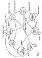
- the state machine depicted in Figure 4 may be implemented by suitable logic within interface controller 50 .
- An underlined signal name indicates that the signal is active low.
- a backslash (/) indicates that the signal is logic low.
- interface controller 50 When interface controller 50 receives a bus request ( BOFF ) from DMA controller 38 , the process proceeds to state 2 .
- interface controller 50 terminates the bus grant to processor 20 by inactivating the bus grant signal ( BG ) and initiates the termination of any cycle in process by activating address acknowledge ( AACK ).
- the process then proceeds to state 3, i n which interface controller 50 completes the termination by deactivating AACK and activating the address retry (ARTRY) signal for one cycle to instruct processor 20 to retry the current transaction (if one is pending) when processor 20 regains control of the bus.
- interface controller 50 turns off the address, data, and control drivers during the transition from state 2 to state 3 .
- DMA controller 38 assumes control of the bus.
- DMA controller 38 will remain bus master as long as it asserts a bus request ( BOFF ).
- BOFF bus request
- the state machine will return to state 2 if SCSI controller 36 requests the bus; otherwise, the state machine will return to state 1.
- SCSI controller 36 is awarded a higher arbitration priority than processor 20 .
- a bus request by processor 20 may be granted higher arbitration priority than a bus request from SCSI controller 36.
- SCSI controller 36 continues to assert a bus request ( M2HOLD ), the process proceeds to state 6 if the bus is not busy as indicated by an inactive address bus busy signal ( ABB ), and no transactions are starting as indicated by an inactive transaction start signal ( TS ).
- interface controller 50 grants control of the bus to SCSI controller 36 ( M2HLDA ).
- SCSI controller 36 transmits a master signal (M2MSTR) to interface controller 50 and terminates its bus request, the process proceeds from state 6 to state 7 , unless DMA controller 38 transmits a bus request. If DMA controller 38 transmits a bus request while the process is at state 6 , the process then proceeds to state 8 . If, however, SCSI controller 36 does not transmit a master signal to interface controller 50 and terminates its bus request, the process returns to state 1 .
- SCSI controller 36 assumes bus mastership and may perform transactions on the bus as long as it asserts its master signal ( M2MSTR ) and DMA controller 38 does not transmit a bus request ( BOFF ). Since processor 20 is assumed to always request the bus, if SCSI controller 36 terminates its master signal, and no bus request is transmitted by DMA controller 38 , the process returns to state 1 . If, however, DMA controller 38 transmits a bus request while SCSI controller 36 masters the bus, the process proceeds to state 8 .
- State 8 represents the termination of bus ownership by SCSI controller 36 due to a bus request from DMA controller 38 .
- interface controller 50 instructs SCSI controller 36 to abort current bus transactions ( M2TEA ) and to turn off its address drivers ( M2RDY ).
- M2TEA abort current bus transactions
- M2RDY address drivers
- the state machine remains in state 8 as long as SCSI controller 36 asserts its master signal.
- SCSI controller 36 terminates its master signal indicating its release of bus mastership, the process proceeds from state 8 to state 3, which has been described. Since SCSI controller 36 has received an abort/error signal (M2TEA), it will retry the aborted transaction once it regains bus master status.
- M2TEA abort/error signal
- bus arbitration implicitly assumes that the bus mastering device which controls the address bus also controls the data bus.
- some processors such as PowerPCTM RISC processors, support bus pipelining to maximize bus utilization.
- address and data tenures are independent and bus mastering devices must arbitrate for control of the address and data busses separately.
- the method of arbitration of the present invention may also be implemented in systems which employ bus pipelining.
- interface controller 50 transmits a signal ( GBL ) to processor 20 during bus transactions for which processor 20 is not the bus master.
- GBL signal
- processor 20 snoops all transactions as either reads or writes with flush, thereby maintaining cache coherency without the additional overhead generated by supporting shared or modified lines.
- the present invention provides an efficient method and system for interfacing a processor which performs transactions utilizing m-byte packets of data to the system bus of a data processing system which performs transactions utilizing n-byte packets of data, where n ⁇ m.
- the present invention provides an scheme for arbitrating between multiple bus masters which have disparate bus acquisition protocols.
Landscapes
- Engineering & Computer Science (AREA)
- Theoretical Computer Science (AREA)
- General Engineering & Computer Science (AREA)
- Physics & Mathematics (AREA)
- General Physics & Mathematics (AREA)
- Computer Hardware Design (AREA)
- Bus Control (AREA)
Applications Claiming Priority (2)
| Application Number | Priority Date | Filing Date | Title |
|---|---|---|---|
| US08/354,701 US5898857A (en) | 1994-12-13 | 1994-12-13 | Method and system for interfacing an upgrade processor to a data processing system |
| US354701 | 1994-12-13 |
Publications (2)
| Publication Number | Publication Date |
|---|---|
| EP0717363A2 true EP0717363A2 (de) | 1996-06-19 |
| EP0717363A3 EP0717363A3 (de) | 1996-09-18 |
Family
ID=23394554
Family Applications (1)
| Application Number | Title | Priority Date | Filing Date |
|---|---|---|---|
| EP95308555A Ceased EP0717363A3 (de) | 1994-12-13 | 1995-11-28 | Anpassung eines Prozessorausbaus an ein Datenverarbeitungssystem |
Country Status (4)
| Country | Link |
|---|---|
| US (2) | US5898857A (de) |
| EP (1) | EP0717363A3 (de) |
| JP (2) | JPH08235106A (de) |
| KR (1) | KR960024918A (de) |
Families Citing this family (25)
| Publication number | Priority date | Publication date | Assignee | Title |
|---|---|---|---|---|
| WO1999052029A1 (fr) * | 1998-04-01 | 1999-10-14 | Omron Corporation | Unite de traitement de donnees et unite de traitement d'images |
| US6085271A (en) * | 1998-04-13 | 2000-07-04 | Sandcraft, Inc. | System bus arbitrator for facilitating multiple transactions in a computer system |
| US6505276B1 (en) | 1998-06-26 | 2003-01-07 | Nec Corporation | Processing-function-provided packet-type memory system and method for controlling the same |
| US6223237B1 (en) * | 1998-07-07 | 2001-04-24 | Adaptive Systems, Inc. | Expandable communications bus |
| US6505259B1 (en) * | 1999-08-27 | 2003-01-07 | Intel Corporation | Reordering of burst data transfers across a host bridge |
| US6782435B2 (en) | 2001-03-26 | 2004-08-24 | Intel Corporation | Device for spatially and temporally reordering for data between a processor, memory and peripherals |
| US6952750B2 (en) * | 2001-05-04 | 2005-10-04 | Texas Instruments Incoporated | Method and device for providing a low power embedded system bus architecture |
| KR100449721B1 (ko) * | 2002-05-20 | 2004-09-22 | 삼성전자주식회사 | 서로 다른 데이터 버스 폭을 갖는 장치들을 위한인터페이스 및 이를 이용한 데이터 전송방법 |
| KR100476895B1 (ko) * | 2002-05-21 | 2005-03-18 | 삼성전자주식회사 | 가변 가능한 데이터 전송 모드를 갖는 인터페이스 장치 및그것의 동작 방법 |
| US7644207B2 (en) * | 2006-08-21 | 2010-01-05 | National Instruments Corporation | High speed bus for isolated data acquisition applications |
| KR100791176B1 (ko) * | 2006-08-28 | 2008-01-02 | 엘지전자 주식회사 | 디지털 데이터 폭 정합을 통한 인터페이스 장치 |
| US7761625B2 (en) * | 2006-09-28 | 2010-07-20 | Virident Systems, Inc. | Methods for main memory with non-volatile type memory modules, and related technologies |
| US7761624B2 (en) * | 2006-09-28 | 2010-07-20 | Virident Systems, Inc. | Systems and apparatus for main memory with non-volatile type memory modules, and related technologies |
| US8074022B2 (en) * | 2006-09-28 | 2011-12-06 | Virident Systems, Inc. | Programmable heterogeneous memory controllers for main memory with different memory modules |
| US7761623B2 (en) * | 2006-09-28 | 2010-07-20 | Virident Systems, Inc. | Main memory in a system with a memory controller configured to control access to non-volatile memory, and related technologies |
| US8051253B2 (en) * | 2006-09-28 | 2011-11-01 | Virident Systems, Inc. | Systems and apparatus with programmable memory control for heterogeneous main memory |
| US7761626B2 (en) * | 2006-09-28 | 2010-07-20 | Virident Systems, Inc. | Methods for main memory in a system with a memory controller configured to control access to non-volatile memory, and related technologies |
| US9984012B2 (en) | 2006-09-28 | 2018-05-29 | Virident Systems, Llc | Read writeable randomly accessible non-volatile memory modules |
| US8949555B1 (en) | 2007-08-30 | 2015-02-03 | Virident Systems, Inc. | Methods for sustained read and write performance with non-volatile memory |
| US20080082750A1 (en) * | 2006-09-28 | 2008-04-03 | Okin Kenneth A | Methods of communicating to, memory modules in a memory channel |
| US8189328B2 (en) * | 2006-10-23 | 2012-05-29 | Virident Systems, Inc. | Methods and apparatus of dual inline memory modules for flash memory |
| US9921896B2 (en) | 2007-08-30 | 2018-03-20 | Virident Systems, Llc | Shutdowns and data recovery to avoid read errors weak pages in a non-volatile memory system |
| US9513695B2 (en) | 2008-06-24 | 2016-12-06 | Virident Systems, Inc. | Methods of managing power in network computer systems |
| US8417873B1 (en) | 2008-06-24 | 2013-04-09 | Virident Systems, Inc. | Random read and read/write block accessible memory |
| US8078771B2 (en) * | 2008-10-31 | 2011-12-13 | Lsi Corporation | Sending large command descriptor block (CDB) structures in serial attached SCSI (SAS) controller |
Family Cites Families (26)
| Publication number | Priority date | Publication date | Assignee | Title |
|---|---|---|---|---|
| US4214302A (en) * | 1978-04-24 | 1980-07-22 | Texas Instruments Incorporated | Eight bit standard connector bus for sixteen bit microcomputer |
| IT1121031B (it) * | 1979-09-19 | 1986-03-26 | Olivetti & Co Spa | Sistema di elaborazione di dati multiprocessore |
| US4716527A (en) * | 1984-12-10 | 1987-12-29 | Ing. C. Olivetti | Bus converter |
| JPS6226561A (ja) * | 1985-07-26 | 1987-02-04 | Toshiba Corp | パ−ソナルコンピユ−タ |
| EP0303751B1 (de) * | 1987-08-20 | 1992-05-20 | International Business Machines Corporation | Schnittstellenmechanismus für Informationsübertragungssteuerung zwischen zwei Vorrichtungen |
| US5142677A (en) * | 1989-05-04 | 1992-08-25 | Texas Instruments Incorporated | Context switching devices, systems and methods |
| US4987529A (en) * | 1988-08-11 | 1991-01-22 | Ast Research, Inc. | Shared memory bus system for arbitrating access control among contending memory refresh circuits, peripheral controllers, and bus masters |
| US5253358A (en) * | 1989-05-19 | 1993-10-12 | Compaq Computer Corporation | Cache memory expansion and transparent interconnection |
| US5162979A (en) * | 1989-10-23 | 1992-11-10 | International Business Machines Corp. | Personal computer processor card interconnect system |
| EP0440452B1 (de) * | 1990-01-31 | 1996-10-09 | Hewlett-Packard Company | Vielfachbus-Systemspeicherarchitektur |
| DE69124437T2 (de) * | 1990-08-09 | 1997-07-03 | Silicon Graphics Inc | Verfahren und Vorrichtung zum Umkehren von Byteordnung in einem Rechner |
| GB9018993D0 (en) * | 1990-08-31 | 1990-10-17 | Ncr Co | Work station interfacing means having burst mode capability |
| JPH05120124A (ja) * | 1990-10-11 | 1993-05-18 | Lsi Logic Corp | マイクロプロセツサ内蔵型のメモリ制御構造 |
| US5257391A (en) * | 1991-08-16 | 1993-10-26 | Ncr Corporation | Disk controller having host interface and bus switches for selecting buffer and drive busses respectively based on configuration control signals |
| US5369748A (en) * | 1991-08-23 | 1994-11-29 | Nexgen Microsystems | Bus arbitration in a dual-bus architecture where one bus has relatively high latency |
| US5291614A (en) * | 1991-09-03 | 1994-03-01 | International Business Machines Corporation | Real-time, concurrent, multifunction digital signal processor subsystem for personal computers |
| WO1993012486A1 (en) * | 1991-12-09 | 1993-06-24 | Tandy Corporation | Direct memory access interface for buses of different width |
| US5265211A (en) * | 1992-01-02 | 1993-11-23 | International Business Machines Corporation | Arbitration control logic for computer system having dual bus architecture |
| US5255376A (en) * | 1992-01-14 | 1993-10-19 | Sun Microsystems, Inc. | Method and apparatus for supporting a dual bit length protocol for data transfers |
| US5313231A (en) * | 1992-03-24 | 1994-05-17 | Texas Instruments Incorporated | Color palette device having big/little endian interfacing, systems and methods |
| US5313595A (en) * | 1992-12-10 | 1994-05-17 | Digital Equipment Corporation | Automatic signal termination system for a computer bus |
| US5649162A (en) * | 1993-05-24 | 1997-07-15 | Micron Electronics, Inc. | Local bus interface |
| US5448704A (en) * | 1994-03-07 | 1995-09-05 | Vlsi Technology, Inc. | Method for performing writes of non-contiguous bytes on a PCI bus in a minimum number of write cycles |
| US5528767A (en) * | 1995-03-21 | 1996-06-18 | United Microelectronics Corp. | Programmable multi-level bus arbitration apparatus in a data processing system |
| US5572686A (en) * | 1995-06-05 | 1996-11-05 | Apple Computer, Inc. | Bus arbitration scheme with priority switching and timer |
| US5799160A (en) * | 1996-06-24 | 1998-08-25 | Motorola, Inc. | Circuit and method for controlling bus arbitration |
-
1994
- 1994-12-13 US US08/354,701 patent/US5898857A/en not_active Expired - Lifetime
-
1995
- 1995-11-17 JP JP7299554A patent/JPH08235106A/ja active Pending
- 1995-11-28 EP EP95308555A patent/EP0717363A3/de not_active Ceased
- 1995-12-08 KR KR1019950047840A patent/KR960024918A/ko not_active Ceased
-
1999
- 1999-02-10 US US09/247,536 patent/US6088750A/en not_active Expired - Fee Related
-
2002
- 2002-03-18 JP JP2002074116A patent/JP2002278921A/ja active Pending
Non-Patent Citations (2)
| Title |
|---|
| "Intel486 Microprocessor Data Book", INTEL CORPORATION |
| "PowerPC 601 RISC Microprocessor User's Manual", IBM CORPORATION |
Also Published As
| Publication number | Publication date |
|---|---|
| JPH08235106A (ja) | 1996-09-13 |
| US5898857A (en) | 1999-04-27 |
| KR960024918A (ko) | 1996-07-20 |
| JP2002278921A (ja) | 2002-09-27 |
| EP0717363A3 (de) | 1996-09-18 |
| US6088750A (en) | 2000-07-11 |
Similar Documents
| Publication | Publication Date | Title |
|---|---|---|
| US6088750A (en) | Method and system for arbitrating between bus masters having diverse bus acquisition protocols | |
| US5664197A (en) | Method and apparatus for handling bus master channel and direct memory access (DMA) channel access requests at an I/O controller | |
| US5729762A (en) | Input output controller having interface logic coupled to DMA controller and plurality of address lines for carrying control information to DMA agent | |
| US6772254B2 (en) | Multi-master computer system with overlapped read and write operations and scalable address pipelining | |
| US6493776B1 (en) | Scalable on-chip system bus | |
| US5398244A (en) | Method and apparatus for reduced latency in hold bus cycles | |
| US5455916A (en) | Method for performing inter-unit data transfer operations among a plurality of input/output bus interface units coupled to a common asynchronous bus | |
| JP4500373B2 (ja) | 一体化システムメモリおよび改良されたバス同時実行性を有するコンピュータシステム | |
| US6493803B1 (en) | Direct memory access controller with channel width configurability support | |
| US6732208B1 (en) | Low latency system bus interface for multi-master processing environments | |
| US5535341A (en) | Apparatus and method for determining the status of data buffers in a bridge between two buses during a flush operation | |
| EP0629955B1 (de) | Arbitrierungslogik für Mehrfachbus-Rechnersystem | |
| US5191656A (en) | Method and apparatus for shared use of a multiplexed address/data signal bus by multiple bus masters | |
| US6636927B1 (en) | Bridge device for transferring data using master-specific prefetch sizes | |
| US5949981A (en) | Deadlock avoidance in a bridge between a split transaction bus and a single envelope bus | |
| US7752374B2 (en) | Method and apparatus for host messaging unit for peripheral component interconnect busmaster devices | |
| JPH0661075B2 (ja) | コンピユータシステム内でデータ転送方法 | |
| EP0658852A2 (de) | Rechnersystem mit verändertem lokalen Datenbus | |
| US5793990A (en) | Multiplex address/data bus with multiplex system controller and method therefor | |
| EP0718772A1 (de) | Verfahren zur Verbesserung der Buslatenz und zum Ermöglichen der Stossdatenübertragung von unbekannter Länge | |
| JPH0330045A (ja) | マイクロプロセツサ用論理回路 | |
| US5890002A (en) | System and method for bus master emulation | |
| EP0651333A1 (de) | Direktspeicherzugriffssteuerung | |
| US6266723B1 (en) | Method and system for optimizing of peripheral component interconnect PCI bus transfers | |
| US20030070018A1 (en) | Delayed transaction method and device used in a PCI system |
Legal Events
| Date | Code | Title | Description |
|---|---|---|---|
| PUAI | Public reference made under article 153(3) epc to a published international application that has entered the european phase |
Free format text: ORIGINAL CODE: 0009012 |
|
| AK | Designated contracting states |
Kind code of ref document: A2 Designated state(s): DE FR GB |
|
| PUAL | Search report despatched |
Free format text: ORIGINAL CODE: 0009013 |
|
| AK | Designated contracting states |
Kind code of ref document: A3 Designated state(s): DE FR GB |
|
| 17P | Request for examination filed |
Effective date: 19961029 |
|
| 17Q | First examination report despatched |
Effective date: 19990812 |
|
| STAA | Information on the status of an ep patent application or granted ep patent |
Free format text: STATUS: THE APPLICATION HAS BEEN REFUSED |
|
| 18R | Application refused |
Effective date: 20020415 |