EP0717471A2 - Federkontaktelemente enthaltender Kontaktfläche-zu-Kontaktfläche Verbinder von hoher Dichte und mit Hochstrom-Kapazität - Google Patents
Federkontaktelemente enthaltender Kontaktfläche-zu-Kontaktfläche Verbinder von hoher Dichte und mit Hochstrom-Kapazität Download PDFInfo
- Publication number
- EP0717471A2 EP0717471A2 EP95118103A EP95118103A EP0717471A2 EP 0717471 A2 EP0717471 A2 EP 0717471A2 EP 95118103 A EP95118103 A EP 95118103A EP 95118103 A EP95118103 A EP 95118103A EP 0717471 A2 EP0717471 A2 EP 0717471A2
- Authority
- EP
- European Patent Office
- Prior art keywords
- connector assembly
- spring contact
- accordance
- contact elements
- retainer
- Prior art date
- Legal status (The legal status is an assumption and is not a legal conclusion. Google has not performed a legal analysis and makes no representation as to the accuracy of the status listed.)
- Withdrawn
Links
Images


Classifications
-
- H—ELECTRICITY
- H01—ELECTRIC ELEMENTS
- H01R—ELECTRICALLY-CONDUCTIVE CONNECTIONS; STRUCTURAL ASSOCIATIONS OF A PLURALITY OF MUTUALLY-INSULATED ELECTRICAL CONNECTING ELEMENTS; COUPLING DEVICES; CURRENT COLLECTORS
- H01R13/00—Details of coupling devices of the kinds covered by groups H01R12/70 or H01R24/00 - H01R33/00
- H01R13/02—Contact members
- H01R13/22—Contacts for co-operating by abutting
- H01R13/24—Contacts for co-operating by abutting resilient; resiliently-mounted
- H01R13/2435—Contacts for co-operating by abutting resilient; resiliently-mounted with opposite contact points, e.g. C beam
-
- H—ELECTRICITY
- H01—ELECTRIC ELEMENTS
- H01R—ELECTRICALLY-CONDUCTIVE CONNECTIONS; STRUCTURAL ASSOCIATIONS OF A PLURALITY OF MUTUALLY-INSULATED ELECTRICAL CONNECTING ELEMENTS; COUPLING DEVICES; CURRENT COLLECTORS
- H01R12/00—Structural associations of a plurality of mutually-insulated electrical connecting elements, specially adapted for printed circuits, e.g. printed circuit boards [PCB], flat or ribbon cables, or like generally planar structures, e.g. terminal strips, terminal blocks; Coupling devices specially adapted for printed circuits, flat or ribbon cables, or like generally planar structures; Terminals specially adapted for contact with, or insertion into, printed circuits, flat or ribbon cables, or like generally planar structures
- H01R12/70—Coupling devices
- H01R12/71—Coupling devices for rigid printing circuits or like structures
- H01R12/712—Coupling devices for rigid printing circuits or like structures co-operating with the surface of the printed circuit or with a coupling device exclusively provided on the surface of the printed circuit
- H01R12/714—Coupling devices for rigid printing circuits or like structures co-operating with the surface of the printed circuit or with a coupling device exclusively provided on the surface of the printed circuit with contacts abutting directly the printed circuit; Button contacts therefore provided on the printed circuit
-
- H—ELECTRICITY
- H05—ELECTRIC TECHNIQUES NOT OTHERWISE PROVIDED FOR
- H05K—PRINTED CIRCUITS; CASINGS OR CONSTRUCTIONAL DETAILS OF ELECTRIC APPARATUS; MANUFACTURE OF ASSEMBLAGES OF ELECTRICAL COMPONENTS
- H05K7/00—Constructional details common to different types of electric apparatus
- H05K7/02—Arrangements of circuit components or wiring on supporting structure
- H05K7/10—Plug-in assemblages of components, e.g. IC sockets
- H05K7/1053—Plug-in assemblages of components, e.g. IC sockets having interior leads
- H05K7/1061—Plug-in assemblages of components, e.g. IC sockets having interior leads co-operating by abutting
- H05K7/1069—Plug-in assemblages of components, e.g. IC sockets having interior leads co-operating by abutting with spring contact pieces
Definitions
- This invention relates to a device for interconnecting two electronic components with large number of individual connections that can be easily disconnected and reconnected, can accommodate surface irregularities and thermal expansion/contraction between the components. A large number implies thousands.
- U.S. Patent No. 4,764,848 issued to Simpson discloses a connector of bent wires which are soldered to both the ceramic chip carrier and the printed circuit board. Each wire has a root at one end and a tip at the other end. The root of each bent wire is attached to the integrated circuit package to form a fixed electrical and mechanical connection. The tip of the bent wire is soldered to a pad on the surface of the printed circuit board. This arrangement provides for strain relief of the connection and mechanically fixes the ceramic device to the board. This disclosure does not provide for an easily removable connector, especially in the customers office.
- U.S. Patent No. 5,248,262 issued to Busacco, et al and U.S. Patent No. 5,061,192 issued to Chapin, et al discloses a connector assembly with small flat beams attached to a flexible film and contained inside a housing.
- the small flat beams are copper etched on a polyamide strip, are placed in and extend through the housing, and make contact with pads on circuit members on opposite sides of the connector assembly.
- This strip of connecting elements is made from several layers of etched or bonded material including a conducting element that contacts the pads, a polyamide backing material, a copper ground plane material and, in the case of Patent No. 5,248,262, a stainless steel spring material bonded to but electrically isolated from the copper ground plane.
- a plurality of the connector elements are contained, and spaced evenly, on the polyamide strip along with the stainless steel spring.
- the housing contains long slots for the strips to protrude through the surface to make contact with pads on circuit members.
- the polyamide film retains the contact elements in a single strip and multiple strips make up a connector assembly. Within a single strip, compliance is limited from contact to contact because of the rigidity of the film in that direction.
- Each contact element has its reacting stresses and strains within its joints set by the amount of its compression and the amount of compression of its adjacent neighbors. As a result, some of the stresses and strains are parallel with the strip and cause shearing to the assembly. To limit the adverse affect of the shearing forces, two precautions must be taken.
- each contact within a strip should be compressed simultaneously, i.e., upon assembly, guides should be used to uniformly force the electronic module upon the array with minimum degree of tilt.
- both sides of the printed circuit board should be utilized which reduces the average wire length and improves the performance of the system.
- the connector assembly must also exhibit the characteristic of low electrical noise since the application will connect very high speed integrated circuits.
- the connector assembly must support large amounts of current in this small area. This leads to a requirement for cooling the connector as power demands are significant.
- the objects of this invention are to improve the interconnectivity performance, density, current carrying capacity and cost of joining in a separable manner an electronic module to a printed circuit board.
- the above objects are realized by utilizing a plurality of SCE as the electrical interconnect.
- the SCE are shaped to provide optimized mechanical forces to assure electrical contact across the electronic module.
- An automated fabrication process as shown in application serial number 325 025, filed on the same day as the present application, entitled “Apparatus and Process for Manufacture of Spring Contact Elements And Assembly Thereof", and assigned to the same assignee as this application, can be implemented to stamp the appropriate shape of the SCE.
- Inherent with the invention are overlapping connector wire segments which, due to the included angle, improve the shielding of the SCE segments.
- the SCEs are not connected to the module or the printed circuit board but are housed in a retainer. In this case, the invention is a separate assembly or field replaceable unit (FRU).
- FRU field replaceable unit
- the present invention can be embodied with attachment to the module or can be attached to the printed circuit board or the ceramic components containing the chips.
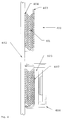
- Figure 1A shows an overview of a cross-section of the completed assembly of this invention in its preferred embodiment.
- Figure 1B shows an isometric view of the same completed assembly shown in Figure 1A.
- Figure 2 contains three view of the SCE.
- Fig. 2A is a top view
- Fig. 2B is a side view
- Fig. 2C is an end view.
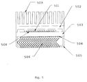
- Figure 3A is a cross-sectional view of the preferred embodiment in which the connector assembly is not attached to either the ceramic component or the printed circuit board.
- Fig. 3B is a top view of the connector assembly.
- Fig. 3C is an exploded view of the cross-section shown in Fig. 3A with the SCE compressed.
- Figure 4 is a cross-sectional view of the embodiment in which the improved connector is attached directly to the printed circuit board.
- Figure 5 illustrates the improved electronic connector embodiment in which it is attached to the bottom surface of a single chip or multi-chip module.
- Figure 6 shows an enhancement to the embodiment described in Figure 4 with the connector assembly attached to both sides of the printed circuit board.
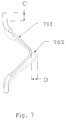
- Figure 7 describes the shape of the SCE when compressed.
- Figure 8 shows a method of cooling the SCE by blowing air through the assembly.
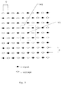
- Figure 9 shows the electrical grid used to evaluate the electrical performance of the connector.
- the present invention relates to an enhanced electronic connector having improved density, current carrying capacity, lower cost, and improved heat dissipation.
- the improved connections comprises a plurality of short SCEs closely spaced together.
- the elements are optimally shaped to provide maintain a large cross-sectional area for reduced electrical resistance while minimizing the mating forces needed to achieve electrical contact between the electronic module and the printed circuit board.
- the shape of the elements may vary with its location in the connector array.
- Fig. 1A is a side cutaway of a high performance multichip module with an improved electronic connector according to the first embodiment of the present invention.
- Fig. 1B represents an isometric expanded view of the same assembly shown in Fig. 1A.
- the module of Fig. 1A and 1B includes an array of integrated circuit chips 101 mounted to a substrate 102.
- the substrate 102 includes pads 108 which are used to establish electrical connections to the pads 105 on the motherboard 109 via the SCEs 104 and are located relative to the pads 105 and 108 by guide pins 107.
- the SCEs 104 are retained by a upper housing 110 and lower housing 103 and their tips 106 extend slightly outside the upper and lower housings. In the assembled position, the SCEs accommodate the application x-y-z tolerances and thermal expansion mismatches and the SCEs are not necessarily identical to one another.
- the connector can house N rows x M columns of SCEs with N and M not necessarily equal.
- N and M not necessarily equal.
- the degree to which the space between the spring contact elements can be reduced is dependent on the ability to manufacture the connector as well as the ability of the motherboard to support the sheer number of interconnections in a small area.
- a typical centerline spacing satisfying these constraints is 1 to 1.5 mm.
- FIGs. 2A, 2B, and 2C A close-up of top, front, and side views of a single SCE are shown in Figs. 2A, 2B, and 2C, respectively.
- the SCE was manufactured from a round cross-sectional wire and formed into the shape shown.
- beryllium copper C17200 half hardened can be the bulk beam material.
- This material is readily available in wire form, widely used as a spring material, has very good workability and soldering properties, and has reasonable electrical conductivity (22% pure copper). Any other material having these attributes is suitable for this invention.
- the bulk material is prehardened by heat treating in an oxygen-free atmosphere and then electroplated with nickel and palladium for resistance to corrosion.
- An automated fabrication process consisting of dicing, stamping, and forming the wire into individual SCE can be employed for mass production. Alternatively (and for prototype hardware), the above process steps can be done manually.
- the SCE ends 201 are gold electroplated for low joint contact resistance.
- the forming tool flattened the round cross-section into a rectangular cross-section 203 at only a prescribed portion centered about the wire tips.
- the SCE was bent to form an included angle 202 and, once completed, the two SCE tips 201 were aligned co-axially.
- This invention allows for optimization of the SCE to the electronic module application by adjusting the wire material, the included angle 202, and the degree of cross-sectional shaping 203.
- An improved electronic connector shown in Figs. 1A and 1B could be comprised of one or multiple part number SCEs for localized force/contact optimization.
- Fig. 3B illustrates the preferred embodiment cross-section with SCE 303 being held in place with retainer halves 301 and 302.
- the mating surface between the two halves is indicated by 305.
- a perforated dielectric separator 311 is located between the rows of SCE 303 to keep them from shorting to each other.
- the retainer halves 301 and 302 are fabricated from a dielectrical material to provide electrical isolation between all SCE 303. If required, air can be forced through the retainer as shown in Figure 3A. This allows for cooling in high current applications.
- the coolant 316 air for example, is pumped through the interior of the retainer halves and flows above, below, and through the perforated separators 311. The heated coolant exhausts at the other end of the retainer at 317.
- the side walls 307 and 308 attached the two retainer halves together and prohibit the coolant from escaping prematurely.
- the coolant entrance and exit sides of the retainer halves may have discrete mating locations for extra large connector applications.
- the grid distances between the SCE, S may vary but is typically between 1 and 1.5 mm as previously stated.
- the outer edges of the retainer are indicated by 307 and 308.
- the tips of the SCE 304 protrude through the retainer and make contact with gold plated pads 105 on the surface of the attaching component as does the other end 306 to pad 108.
- the holes 314 are countersunk on the inside of the retainer halves to keep the SCEs 303 from binding on the inside of the retainers.
- the overall height of the connector assembly, H is typically between 4.5 and 7.5 mm.
- Fig 3B shows the SCE 303 in the uncompressed position.
- Fig. 3C is an enlarged view of Fig 3B showing the SCE in an exaggerated compressed position. Sufficient clearance is provided by the countersunk holes 314 as depicted. Not shown are the upper and lower electronic modules which applies the compressing force upon the SCEs 303.
- Fig. 3C also illustrates the embodiment in which the spacing 310 between SCEs 303 need not be uniform across the array. This is also true for the direction in to and out of the plane illustrated in the figure.
- Fig. 4 illustrates an embodiment where the improved electronic module connector 410 is attached directly to the printed circuit board 402.
- a single housing 403 is used to retain and protect the array of SCEs. Small x-y adjustments to the SCE array can be made during the installation of the retainer/plenum 403.
- the SCE tips are attached to the printed circuit board by a solder joint 404 and inspection of the joints can be performed by conventional inspection methods.
- the contact pads of the printed circuit board may be at finer spacings than the plated through holes provided that surface wiring is present to route the lines to vias for access to the internal wires.
- the high performance contact to the electronic module 405 occurs as the module is compressed against and held in place with a spring retention clip 406. As previously noted, the ends of the SCE 401 are compressed against the gold pads 407 on the surface of the module.
- the connector assembly 410 becomes part of the printed circuit board 402 field replacement unit (FRU).
- FRU field replacement unit
- FIG. 5 shows a integrated chip 501 attached to the opposite side of the base of the component 503 from the connector with a very dense array of solder balls 508.
- the chip is encapsulated with a cooling frame 502, and for high powered applications, a heat sink 509 is attached.
- the air flow used to cool the highly integrated chip can also cool the SCE 506 is required.
- spring contact elements 506 are attached (soldered or any other suitable method) to the component 503 at 504 and become part of the FRU.
- the SCEs 506 protrude beyond the retainer 505 and make contact to pads on the printed circuit board.
- the retainer 505 is aligned to the electronic component 503 and held in place with an adhesive or some other mechanical method. This embodiment permits the SCE 506 to be on a smaller FRU and one that is easily replaceable.
- FIG. 6 illustrates an embodiment in which connectors with SCEs are applied to this application.
- a printed circuit board 602 has and array of SCEs 601 soldered at 606 on one surface and an array of SCEs 603 soldered to the other surface at 604.
- the SCEs 601 and 603 may share the same plated-through-holes 607 located in the board.
- the SCEs are soldered at blind via 608 locations or on surface lands (not shown) similar to 404 of Fig. 4. This embodiment reduces the interconnect wire lengths between high performance integrated chips and also reduces the printed circuit board 602 size.
- a finite element model was constructed to analyze the force deflection characteristics of the variable cross-section SCE.
- FEM linear beam elements were used with each element indexed to its appropriate cross-sectional area property table.
- the node of the SCE coincident with the board was held fixed in both displacement and rotation.
- the node representing the SCE contact was displaced by variable amounts and its rotation was kept free.
- the curvature of the SCE was modeled by using many linear beam elements in a faceted manner.
- the pertinent material properties for the BeCu bulk material include Young's modulus and Poisson's ratio.
- these variables are approximately 127.5 GPa and 0.29 respectively.
- a minimum contact load for a reliable and repeatable contact is 30 grams for this area.
- An example of results from the FEM analysis for a 90 degree included angle, 0.25 mm diameter wire, and a 60 percent stamping compression for the center portion of the SCE reveals 0.1 mm as the minimum deflection to achieve the minimum loading.
- the maximum deflection is dependent on a tolerance analysis of the appropriate mounting hardware (i.e., board flatness, stiffener, substrate flatness, baseplate, etc.) and is system dependent. For illustrative purposes only, a maximum deflection of 0.3 mm is applied here.
- the maximum contact loading is 70 grams which is consistent with today's state-of-the-art area array connectors.
- Fig. 7 shows typical FEM output of the deformed geometry with an exaggerated scale so that the deflection can be discerned.
- the SCE is compressed by a displacement, C, which results in an lateral movement of distance D (approx .25 mm).
- D approximately a displacement of distance
- the maximum loading is reduced to about 60 grams.
- Another geometry examined is one which the cross-sectional area is increased for reduced DC resistance. For this case, a 0.38 mm diameter wire is formed to a .15x.74 mm rectangular cross-section.
- the flattening of the wire is a means to lower the spring rate of the larger diameter SCE to acceptable levels.
- the spring rate of the SCE can be controlled by simple changes to its geometry.
- a customized SCE connector can consist of variable spring rate SCEs -- i.e., the center and perimeter of the area array can have different spring rates to minimize substrate deflections while maintaining sufficient contact loads.
- the DC resistance for the rectangular SCE stated above (.15x.74mm) comprises of a bulk value of 6.5 milliohms and a contact resistance value between 2 milliohms ("Clean”) and 4.1 milliohms ("Dust").
- the total connector resistance range for contact loading between 30 and 70 grams is 8.5 to 10.6 milliohms for this example.
- a worst case heat generation rate will be 0.011 Watts per 1 amp power contact.
- approximately 16.5 Watts of power is dissipated in SCEs if 50% of the SCE carry power at the aforementioned rate. Referring to Fig.
- cooling of the connector is achieved by pumping a coolant in at 316, through the SCE array serially, and exhausting at the other end 317.
- the copper SCEs behave as pin fins with a uniform heat generation rate.
- FIG. 8 shows how an air deflector 805 with impinged air can be used to direct the air flow into the connector assembly 804.
- the air deflector 805 is secured to the printed circuit board 801 with an adhesive. Air is directed from a fan 806 or by some other means on to the deflector 805 and then into the connector assembly 804 through the opening at 807. Air exits at the other side of the assembly 808.
- the chips 803 and the ceramic component 802 are cooled by their own heat sinks in a dedicated air stream for that purpose.
- the deflector 805 would also be used as a board stiffener when mounting heavy ceramic components 802.
- the electrical performance of this connector design was determined using multiple electrical analysis finite difference tools.
- a 3x3 array of SCEs with the center and corner locations as the signal lines 901 was used as the calculation domain as shown in Fig. 9 by the dashed box 902.
- the dimensions S and T were 1.2 mm for the comparison to a tuning fork type connector presently used extensively for a high performance mainframe application.
- One 3-dimensional code was used to estimate the self and mutual inductances of each segment of the SCEs.
- Another code was used to reduce the hundreds of inductances to a matrix of 9x9 inductances accounting for di/dt direction through the conductors (i.e., signals v reference).
- the usage of the SCEs in a horizontally and vertically alternating signal/reference pattern forms the grid. This pattern aids shielding of the signals from one another. Additional shielding occurs in the connector because the shape of the SCE coupled with a tight spacing causes some overlapping of segments of the wire. These overlapping segments also alternate signal and reference usage but because of the included angle, their relative spacing is less than that at the SCE ends. Hence, the combination of overlapping SCEs and the SCE shape reduces the self inductance and further shields the signal lines.
Landscapes
- Engineering & Computer Science (AREA)
- Microelectronics & Electronic Packaging (AREA)
- Coupling Device And Connection With Printed Circuit (AREA)
- Multi-Conductor Connections (AREA)
Applications Claiming Priority (2)
| Application Number | Priority Date | Filing Date | Title |
|---|---|---|---|
| US355564 | 1994-12-14 | ||
| US08/355,564 US5611696A (en) | 1994-12-14 | 1994-12-14 | High density and high current capacity pad-to-pad connector comprising of spring connector elements (SCE) |
Publications (1)
| Publication Number | Publication Date |
|---|---|
| EP0717471A2 true EP0717471A2 (de) | 1996-06-19 |
Family
ID=23397901
Family Applications (1)
| Application Number | Title | Priority Date | Filing Date |
|---|---|---|---|
| EP95118103A Withdrawn EP0717471A2 (de) | 1994-12-14 | 1995-11-17 | Federkontaktelemente enthaltender Kontaktfläche-zu-Kontaktfläche Verbinder von hoher Dichte und mit Hochstrom-Kapazität |
Country Status (5)
| Country | Link |
|---|---|
| US (1) | US5611696A (de) |
| EP (1) | EP0717471A2 (de) |
| JP (1) | JP2843786B2 (de) |
| CN (1) | CN1044950C (de) |
| MY (1) | MY112913A (de) |
Cited By (4)
| Publication number | Priority date | Publication date | Assignee | Title |
|---|---|---|---|---|
| WO2000003573A1 (en) * | 1998-07-13 | 2000-01-20 | Unisys Corporation | Integrated circuit module having springy contacts of at least two different types for reduced stress, and subassembly for such module |
| WO2000033427A1 (en) * | 1998-11-30 | 2000-06-08 | Intel Corporation | Controlling the heat expansion of electrical couplings |
| CN103022774A (zh) * | 2012-12-28 | 2013-04-03 | 中国人民解放军国防科学技术大学 | 星箭分离连接器 |
| CN106033838A (zh) * | 2015-03-16 | 2016-10-19 | 华为技术有限公司 | 线缆和天线 |
Families Citing this family (31)
| Publication number | Priority date | Publication date | Assignee | Title |
|---|---|---|---|---|
| US5810607A (en) * | 1995-09-13 | 1998-09-22 | International Business Machines Corporation | Interconnector with contact pads having enhanced durability |
| US6835898B2 (en) * | 1993-11-16 | 2004-12-28 | Formfactor, Inc. | Electrical contact structures formed by configuring a flexible wire to have a springable shape and overcoating the wire with at least one layer of a resilient conductive material, methods of mounting the contact structures to electronic components, and applications for employing the contact structures |
| US5772451A (en) | 1993-11-16 | 1998-06-30 | Form Factor, Inc. | Sockets for electronic components and methods of connecting to electronic components |
| US20070228110A1 (en) * | 1993-11-16 | 2007-10-04 | Formfactor, Inc. | Method Of Wirebonding That Utilizes A Gas Flow Within A Capillary From Which A Wire Is Played Out |
| US6727579B1 (en) | 1994-11-16 | 2004-04-27 | Formfactor, Inc. | Electrical contact structures formed by configuring a flexible wire to have a springable shape and overcoating the wire with at least one layer of a resilient conductive material, methods of mounting the contact structures to electronic components, and applications for employing the contact structures |
| TW441227B (en) * | 1995-05-26 | 2001-06-16 | E Tec Ag | Contact arrangement for detachably attaching an electric component, especially an integrated circuit to a printed circuit board |
| US20100065963A1 (en) * | 1995-05-26 | 2010-03-18 | Formfactor, Inc. | Method of wirebonding that utilizes a gas flow within a capillary from which a wire is played out |
| US5724229A (en) * | 1996-03-27 | 1998-03-03 | Unisys Corporation | Electromechanical assembly having a lid which protects IC chips and holds contact springs |
| CH693478A5 (fr) | 1996-05-10 | 2003-08-15 | E Tec Ag | Socle de connexion de deux composants électriques. |
| US6024579A (en) * | 1998-05-29 | 2000-02-15 | The Whitaker Corporation | Electrical connector having buckling beam contacts |
| US6441315B1 (en) * | 1998-11-10 | 2002-08-27 | Formfactor, Inc. | Contact structures with blades having a wiping motion |
| JP2000168467A (ja) * | 1998-12-02 | 2000-06-20 | Yazaki Corp | 回路体への接続構造 |
| JP3288654B2 (ja) * | 1999-07-23 | 2002-06-04 | ヒロセ電機株式会社 | 電気コネクタの製造方法 |
| US6434817B1 (en) | 1999-12-03 | 2002-08-20 | Delphi Technologies, Inc. | Method for joining an integrated circuit |
| US6848942B1 (en) | 2000-01-12 | 2005-02-01 | Molex Incorporated | Connectors having supportive barrier components |
| US6596948B1 (en) * | 2000-04-28 | 2003-07-22 | Hewlett-Packard Development Company, L.P. | Processor and power supply circuit |
| US6426638B1 (en) | 2000-05-02 | 2002-07-30 | Decision Track Llc | Compliant probe apparatus |
| JP2001326046A (ja) * | 2000-05-17 | 2001-11-22 | Enplas Corp | コンタクトピン集合体、コンタクトピン組立体及び電気部品用ソケット |
| US6774315B1 (en) * | 2000-05-24 | 2004-08-10 | International Business Machines Corporation | Floating interposer |
| US6331836B1 (en) * | 2000-08-24 | 2001-12-18 | Fast Location.Net, Llc | Method and apparatus for rapidly estimating the doppler-error and other receiver frequency errors of global positioning system satellite signals weakened by obstructions in the signal path |
| ATE371196T1 (de) * | 2002-03-05 | 2007-09-15 | Rika Denshi America Inc | Vorrichtung für eine schnittstelle zwischen elektronischen gehäusen und testgeräten |
| US6839965B2 (en) * | 2003-02-06 | 2005-01-11 | R-Tec Corporation | Method of manufacturing a resistor connector |
| US6832917B1 (en) | 2004-01-16 | 2004-12-21 | Intercon Systems, Inc. | Interposer assembly |
| US7753740B2 (en) | 2007-07-20 | 2010-07-13 | Numatics, Incorporated | Modular electrical bus system |
| US8074680B2 (en) | 2008-03-28 | 2011-12-13 | Numatics, Incorporated | Modular electrical bus system with built in ground circuit |
| US7520753B1 (en) | 2008-03-31 | 2009-04-21 | International Business Machines Corporation | Method of using coil contact as electrical interconnect |
| US8399983B1 (en) * | 2008-12-11 | 2013-03-19 | Xilinx, Inc. | Semiconductor assembly with integrated circuit and companion device |
| DE102010062580A1 (de) * | 2010-12-08 | 2012-06-14 | Bayerische Motoren Werke Aktiengesellschaft | Hochstrom-Steckverbinder |
| TWI543451B (zh) * | 2013-07-30 | 2016-07-21 | 鴻海精密工業股份有限公司 | 電連接器及其組合 |
| CN109417849B (zh) * | 2016-07-12 | 2021-08-17 | Abb电网瑞士股份公司 | 电流分离装置 |
| EP3522306B1 (de) * | 2018-01-31 | 2020-09-02 | ODU GmbH & Co. KG | Verbindungsmodul und verbinder zur übertragung von hf-signalen |
Family Cites Families (5)
| Publication number | Priority date | Publication date | Assignee | Title |
|---|---|---|---|---|
| US3921285A (en) * | 1974-07-15 | 1975-11-25 | Ibm | Method for joining microminiature components to a carrying structure |
| US4764848A (en) * | 1986-11-24 | 1988-08-16 | International Business Machines Corporation | Surface mounted array strain relief device |
| US5123848A (en) * | 1990-07-20 | 1992-06-23 | Cray Research, Inc. | Computer signal interconnect apparatus |
| US5061192A (en) * | 1990-12-17 | 1991-10-29 | International Business Machines Corporation | High density connector |
| US5248262A (en) * | 1992-06-19 | 1993-09-28 | International Business Machines Corporation | High density connector |
-
1994
- 1994-12-14 US US08/355,564 patent/US5611696A/en not_active Expired - Fee Related
-
1995
- 1995-06-20 CN CN95107537A patent/CN1044950C/zh not_active Expired - Fee Related
- 1995-06-29 MY MYPI95001800A patent/MY112913A/en unknown
- 1995-11-17 EP EP95118103A patent/EP0717471A2/de not_active Withdrawn
- 1995-11-27 JP JP7307862A patent/JP2843786B2/ja not_active Expired - Lifetime
Cited By (7)
| Publication number | Priority date | Publication date | Assignee | Title |
|---|---|---|---|---|
| WO2000003573A1 (en) * | 1998-07-13 | 2000-01-20 | Unisys Corporation | Integrated circuit module having springy contacts of at least two different types for reduced stress, and subassembly for such module |
| WO2000033427A1 (en) * | 1998-11-30 | 2000-06-08 | Intel Corporation | Controlling the heat expansion of electrical couplings |
| US6221459B1 (en) | 1998-11-30 | 2001-04-24 | Intel Corporation | Controlling the heat expansion of electrical couplings |
| CN103022774A (zh) * | 2012-12-28 | 2013-04-03 | 中国人民解放军国防科学技术大学 | 星箭分离连接器 |
| CN103022774B (zh) * | 2012-12-28 | 2015-01-21 | 中国人民解放军国防科学技术大学 | 星箭分离连接器 |
| CN106033838A (zh) * | 2015-03-16 | 2016-10-19 | 华为技术有限公司 | 线缆和天线 |
| CN106033838B (zh) * | 2015-03-16 | 2019-03-08 | 华为技术有限公司 | 线缆和天线 |
Also Published As
| Publication number | Publication date |
|---|---|
| MY112913A (en) | 2001-10-31 |
| US5611696A (en) | 1997-03-18 |
| JPH08222333A (ja) | 1996-08-30 |
| CN1044950C (zh) | 1999-09-01 |
| JP2843786B2 (ja) | 1999-01-06 |
| CN1128417A (zh) | 1996-08-07 |
Similar Documents
| Publication | Publication Date | Title |
|---|---|---|
| US5611696A (en) | High density and high current capacity pad-to-pad connector comprising of spring connector elements (SCE) | |
| US4620761A (en) | High density chip socket | |
| US6046911A (en) | Dual substrate package assembly having dielectric member engaging contacts at only three locations | |
| US5210939A (en) | Lead grid array integrated circuit | |
| US5007841A (en) | Integrated-circuit chip interconnection system | |
| US6916181B2 (en) | Remountable connector for land grid array packages | |
| US4751199A (en) | Process of forming a compliant lead frame for array-type semiconductor packages | |
| US4906194A (en) | High density connector for an IC chip carrier | |
| US5810607A (en) | Interconnector with contact pads having enhanced durability | |
| US7113408B2 (en) | Contact grid array formed on a printed circuit board | |
| US7070419B2 (en) | Land grid array connector including heterogeneous contact elements | |
| US5600178A (en) | Semiconductor package having interdigitated leads | |
| US6014313A (en) | Packaging structure for integrated circuits | |
| US20040253875A1 (en) | Circuitized connector for land grid array | |
| EP0701298A2 (de) | Oberflächenmontierbarer Verbinder mit niedriger Impedanz zum Verbinden von Schaltungsteilen und dessen Verwendung | |
| US20020114129A1 (en) | Ultra-low impedance power interconnection system for electronic packages | |
| US5608966A (en) | Process for manufacture of spring contact elements and assembly thereof | |
| US6684493B2 (en) | Vertically mountable interposer, assembly and method | |
| JP4988132B2 (ja) | 低コストかつ高信頼性適用のための高信頼性インタポーザ | |
| EP0354708A2 (de) | Allgemeine dreidimensionale Packung | |
| US6614246B1 (en) | Probe structure | |
| US7293995B2 (en) | Electrical contact and connector system | |
| EP1637019B1 (de) | Lga steckverbinder | |
| US6016852A (en) | Leaded grid array IC package having coplanar bent leads for surface mount technology | |
| US6365437B2 (en) | Method of connecting a die in an integrated circuit module |
Legal Events
| Date | Code | Title | Description |
|---|---|---|---|
| PUAI | Public reference made under article 153(3) epc to a published international application that has entered the european phase |
Free format text: ORIGINAL CODE: 0009012 |
|
| AK | Designated contracting states |
Kind code of ref document: A2 Designated state(s): DE FR GB |
|
| STAA | Information on the status of an ep patent application or granted ep patent |
Free format text: STATUS: THE APPLICATION HAS BEEN WITHDRAWN |
|
| 18W | Application withdrawn |
Withdrawal date: 19961029 |