EP0718668A2 - Commutateur optique spatial à longueur réduite - Google Patents
Commutateur optique spatial à longueur réduite Download PDFInfo
- Publication number
- EP0718668A2 EP0718668A2 EP95119685A EP95119685A EP0718668A2 EP 0718668 A2 EP0718668 A2 EP 0718668A2 EP 95119685 A EP95119685 A EP 95119685A EP 95119685 A EP95119685 A EP 95119685A EP 0718668 A2 EP0718668 A2 EP 0718668A2
- Authority
- EP
- European Patent Office
- Prior art keywords
- waveguide
- curved
- optical space
- space switch
- regions
- Prior art date
- Legal status (The legal status is an assumption and is not a legal conclusion. Google has not performed a legal analysis and makes no representation as to the accuracy of the status listed.)
- Withdrawn
Links
- 230000003287 optical effect Effects 0.000 title claims description 19
- 239000000758 substrate Substances 0.000 claims abstract description 6
- 238000000576 coating method Methods 0.000 description 2
- 230000010354 integration Effects 0.000 description 2
- 238000004904 shortening Methods 0.000 description 2
- 230000008878 coupling Effects 0.000 description 1
- 238000010168 coupling process Methods 0.000 description 1
- 238000005859 coupling reaction Methods 0.000 description 1
- 230000000694 effects Effects 0.000 description 1
- 238000005516 engineering process Methods 0.000 description 1
- 239000000835 fiber Substances 0.000 description 1
- 239000003365 glass fiber Substances 0.000 description 1
Images
Classifications
-
- G—PHYSICS
- G02—OPTICS
- G02F—OPTICAL DEVICES OR ARRANGEMENTS FOR THE CONTROL OF LIGHT BY MODIFICATION OF THE OPTICAL PROPERTIES OF THE MEDIA OF THE ELEMENTS INVOLVED THEREIN; NON-LINEAR OPTICS; FREQUENCY-CHANGING OF LIGHT; OPTICAL LOGIC ELEMENTS; OPTICAL ANALOGUE/DIGITAL CONVERTERS
- G02F1/00—Devices or arrangements for the control of the intensity, colour, phase, polarisation or direction of light arriving from an independent light source, e.g. switching, gating or modulating; Non-linear optics
- G02F1/29—Devices or arrangements for the control of the intensity, colour, phase, polarisation or direction of light arriving from an independent light source, e.g. switching, gating or modulating; Non-linear optics for the control of the position or the direction of light beams, i.e. deflection
- G02F1/31—Digital deflection, i.e. optical switching
- G02F1/313—Digital deflection, i.e. optical switching in an optical waveguide structure
- G02F1/3137—Digital deflection, i.e. optical switching in an optical waveguide structure with intersecting or branching waveguides, e.g. X-switches and Y-junctions
-
- G—PHYSICS
- G02—OPTICS
- G02B—OPTICAL ELEMENTS, SYSTEMS OR APPARATUS
- G02B6/00—Light guides; Structural details of arrangements comprising light guides and other optical elements, e.g. couplings
- G02B6/10—Light guides; Structural details of arrangements comprising light guides and other optical elements, e.g. couplings of the optical waveguide type
- G02B6/12—Light guides; Structural details of arrangements comprising light guides and other optical elements, e.g. couplings of the optical waveguide type of the integrated circuit kind
- G02B6/122—Basic optical elements, e.g. light-guiding paths
- G02B6/125—Bends, branchings or intersections
-
- G—PHYSICS
- G02—OPTICS
- G02B—OPTICAL ELEMENTS, SYSTEMS OR APPARATUS
- G02B6/00—Light guides; Structural details of arrangements comprising light guides and other optical elements, e.g. couplings
- G02B6/10—Light guides; Structural details of arrangements comprising light guides and other optical elements, e.g. couplings of the optical waveguide type
- G02B6/12—Light guides; Structural details of arrangements comprising light guides and other optical elements, e.g. couplings of the optical waveguide type of the integrated circuit kind
- G02B2006/12133—Functions
- G02B2006/12145—Switch
Definitions
- the invention relates to an optical space switch according to the preamble of patent claim 1.
- Optical space switches are required when light of a predetermined wavelength or light consisting of a superimposition of light of several wavelengths is to be selectively transferred from a single incoming waveguide to one or to a selection from a multiplicity of outgoing waveguides.
- controllable, active waveguide regions are added to the branching arms of simple waveguide branches, and the controllable branches thus created are then cascaded in series.
- Each branch is controlled electrically so that the light radiated into the desired branch arm is amplified, but the light radiated into the other branch arm is absorbed or at least weakened, so that the branch operates as an optical changeover switch.
- a cascade of such branches can also function as an optical distributor if light is amplified in several parallel branch arms.
- a cascaded room switch of this type is e.g. described in DE 43 04 993 A1.
- the controlled active areas are formed there as straight waveguide pieces (FIGS. 1 and 2) and are connected to one another by straight or, where necessary, by curved passive waveguide areas. Also those in the above Publications cited in column 1, paragraph 1 and paragraph 2 of DE 43 04 993 A1 only show optical switches with straight optically active waveguide regions.
- curved active areas can be curved more and are therefore shorter than corresponding passive waveguides in order to achieve the same distance of the outgoing waveguides from one another.
- Curved active welder leader areas are e.g. already known in connection with so-called Y lasers (see, for example, article by O. Hildebrand et al in "Journal of Lightwave Technology", Vol. 11, No. 12, December 1993, pages 2066 to 2072, in particular paragraph VII on page 2071)
- Y lasers see, for example, article by O. Hildebrand et al in "Journal of Lightwave Technology", Vol. 11, No. 12, December 1993, pages 2066 to 2072, in particular paragraph VII on page 2071
- they are not assigned to the individual branching arms as is necessary for the invention, but rather belong to the actual branching as well as parts of the central area surrounding the waveguide.
- the active arm segments adjoining the central area must therefore be used to separately control the branch arms. This means that they cannot be saved to shorten the room switch.
- the individual branches can be made much shorter, which means that a substrate can accommodate significantly more optical branches than when the active areas are formed as straight waveguide pieces.
- Embodiments of the optical space switch according to the invention are specified in the subclaims.
- Claim 2 thus contains a regulation for an advantageous dimensioning of the curved active waveguide regions which permits a high degree of integration.
- Claim 3 relates to a measure that reduces scattering losses of light that occur as a result of the curvatures in the curved waveguide regions.
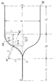
- the figure shows a simple optical branching with an incoming optical waveguide A, which branches at a point V into two outgoing waveguides B1 and B2.
- the two outgoing waveguides have a distance d from one another in their straight parts and run symmetrically with respect to an axis S which runs in the direction of the extension of the incoming waveguide A.
- the incoming waveguide A contributes the amount l1, the area of the curved sections of the outgoing waveguides B1 and B2 the amount l2 and the area of the straight sections of the outgoing waveguide the amount l3.
- Optically active areas AB of the simple branching shown are formed by the curved sections of the outgoing waveguides B1 and B2.
- the length l 2 of the region of the branching which contains the curved waveguide parts can be designed to be less than 130 ⁇ m, which is a considerable shortening compared to curved regions formed from passive waveguides , which are usually> 2 mm long. In addition to this shortening, there is the saving in length, which occurs because optically active, straight waveguide pieces are no longer required. This length saving is again approx. 250 ⁇ m per branching step.
- the active and passive waveguide regions can be produced in a single coating process by using coating methods which allow layers of different thicknesses to be grown in locally delimited regions.
- Scattering losses in the curved active waveguide areas are reduced by making the waveguides wider there than in straight waveguide areas.
Landscapes
- Physics & Mathematics (AREA)
- General Physics & Mathematics (AREA)
- Optics & Photonics (AREA)
- Nonlinear Science (AREA)
- Engineering & Computer Science (AREA)
- Microelectronics & Electronic Packaging (AREA)
- Optical Integrated Circuits (AREA)
Applications Claiming Priority (2)
| Application Number | Priority Date | Filing Date | Title |
|---|---|---|---|
| DE19944445848 DE4445848A1 (de) | 1994-12-22 | 1994-12-22 | Optischer Raumschalter mit kurzer Baulänge |
| DE4445848 | 1994-12-22 |
Publications (2)
| Publication Number | Publication Date |
|---|---|
| EP0718668A2 true EP0718668A2 (fr) | 1996-06-26 |
| EP0718668A3 EP0718668A3 (fr) | 1996-12-18 |
Family
ID=6536621
Family Applications (1)
| Application Number | Title | Priority Date | Filing Date |
|---|---|---|---|
| EP95119685A Withdrawn EP0718668A3 (fr) | 1994-12-22 | 1995-12-14 | Commutateur optique spatial à longueur réduite |
Country Status (2)
| Country | Link |
|---|---|
| EP (1) | EP0718668A3 (fr) |
| DE (1) | DE4445848A1 (fr) |
Cited By (1)
| Publication number | Priority date | Publication date | Assignee | Title |
|---|---|---|---|---|
| US6512860B2 (en) | 2000-08-18 | 2003-01-28 | Danmarks Tekniske Universitet | Bent electro-absorption modulator |
Families Citing this family (1)
| Publication number | Priority date | Publication date | Assignee | Title |
|---|---|---|---|---|
| DE19952216B4 (de) * | 1999-10-29 | 2009-04-02 | Carl Zeiss Meditec Ag | Anordnung zur Leistungsregelung und -überwachung von durch eine oder mehrere optische Faser(n) übertragener Strahlung |
Citations (3)
| Publication number | Priority date | Publication date | Assignee | Title |
|---|---|---|---|---|
| JPS5897028A (ja) * | 1981-12-04 | 1983-06-09 | Oki Electric Ind Co Ltd | 光導波路スイツチ |
| JPS6191623A (ja) * | 1984-10-12 | 1986-05-09 | Nippon Telegr & Teleph Corp <Ntt> | 光スイツチ素子 |
| EP0444721A1 (fr) * | 1990-01-29 | 1991-09-04 | Koninklijke KPN N.V. | Séparateur de polarisation à optique intégrée |
Family Cites Families (1)
| Publication number | Priority date | Publication date | Assignee | Title |
|---|---|---|---|---|
| DE4304993A1 (de) * | 1993-02-18 | 1994-08-25 | Sel Alcatel Ag | Verfahren zur Herstellung eines kaskadierten optischen Raumschalters und nach diesem Verfahren hergestellter kaskadierter optischer Raumschalter |
-
1994
- 1994-12-22 DE DE19944445848 patent/DE4445848A1/de not_active Withdrawn
-
1995
- 1995-12-14 EP EP95119685A patent/EP0718668A3/fr not_active Withdrawn
Patent Citations (3)
| Publication number | Priority date | Publication date | Assignee | Title |
|---|---|---|---|---|
| JPS5897028A (ja) * | 1981-12-04 | 1983-06-09 | Oki Electric Ind Co Ltd | 光導波路スイツチ |
| JPS6191623A (ja) * | 1984-10-12 | 1986-05-09 | Nippon Telegr & Teleph Corp <Ntt> | 光スイツチ素子 |
| EP0444721A1 (fr) * | 1990-01-29 | 1991-09-04 | Koninklijke KPN N.V. | Séparateur de polarisation à optique intégrée |
Non-Patent Citations (3)
| Title |
|---|
| MARCATILI E A J: "Bends in Optical Dielectric Guides", BELL SYSTEM TECHNICAL JOURNAL, vol. 48, no. 7, September 1969 (1969-09-01), NEW YORK, pages 2103 - 2132, XP001367467 * |
| PATENT ABSTRACTS OF JAPAN vol. 007, no. 198 (P - 220) 2 September 1983 (1983-09-02) * |
| PATENT ABSTRACTS OF JAPAN vol. 010, no. 266 (P - 496) 11 September 1986 (1986-09-11) * |
Cited By (1)
| Publication number | Priority date | Publication date | Assignee | Title |
|---|---|---|---|---|
| US6512860B2 (en) | 2000-08-18 | 2003-01-28 | Danmarks Tekniske Universitet | Bent electro-absorption modulator |
Also Published As
| Publication number | Publication date |
|---|---|
| EP0718668A3 (fr) | 1996-12-18 |
| DE4445848A1 (de) | 1996-06-27 |
Similar Documents
| Publication | Publication Date | Title |
|---|---|---|
| DE69318378T2 (de) | Optische Vorrichtung zum Mischen und Verteilen von Licht | |
| DE60320330T2 (de) | Ein optischer Wellenleiter, ein optisches Bauelement und ein optischer Schalter | |
| EP0037006B1 (fr) | Coupleur-étoile optique avec dispositif mélangeur planaire | |
| DE602004000098T2 (de) | Optische Wellenleiteranordnung mit reduzierten Überkreuzungsverlusten | |
| WO1996013884A1 (fr) | Dispositif de guidage et de façonnage des faisceaux emis par une rangee rectiligne de diodes laser | |
| DE68914349T2 (de) | Methode zur Herstellung eines optischen Verzweigungs- und Kopplungselements. | |
| EP0560412A2 (fr) | Dispositif de spectromètre optique intégré et son procédé de fabrication | |
| EP0863588A2 (fr) | Optique pour laser et laser à diode | |
| EP0629297A1 (fr) | Composant optique integre. | |
| DE69924707T2 (de) | Abstimmbarer optischer einfüge-/ausblendmultiplexer | |
| DE2910291A1 (de) | Bauelement mit optischen lichtwellenleitern | |
| DE60122247T2 (de) | Optischer Multiplexer/Demultiplexer | |
| DE69625838T2 (de) | Ausrichten von optischen Fasern | |
| EP1070271B1 (fr) | Configuration destinee a la separation et/ou la reunion spatiale de canaux de longueurs d'ondes optiques | |
| DE2905916A1 (de) | Faseroptische uebertragungsvorrichtung | |
| DE60307610T2 (de) | Optischer koppler | |
| EP0822424B1 (fr) | Dispositif de branchement optique | |
| EP0831343A2 (fr) | Guide d'ondes optique et son procédé de fabrication | |
| EP0718668A2 (fr) | Commutateur optique spatial à longueur réduite | |
| EP0903823B1 (fr) | Elément laser comprenant un réseau de lasers et méthode de fabrication | |
| DE3829540C2 (de) | Gebogener Wellenleiter für eine integrierte optische Schaltung | |
| WO2016050898A1 (fr) | Fibre optique | |
| EP1076252A1 (fr) | Interféromètre optique intégré préréglé à plusieurs faisceaux | |
| DE69737491T2 (de) | Integrierte optische Einrichtung mit aktiven und passiven Wellenleiterbereichen | |
| DE10054370A1 (de) | Optisches Verteilerelement |
Legal Events
| Date | Code | Title | Description |
|---|---|---|---|
| PUAI | Public reference made under article 153(3) epc to a published international application that has entered the european phase |
Free format text: ORIGINAL CODE: 0009012 |
|
| AK | Designated contracting states |
Kind code of ref document: A2 Designated state(s): DE ES FR GB IT |
|
| PUAL | Search report despatched |
Free format text: ORIGINAL CODE: 0009013 |
|
| AK | Designated contracting states |
Kind code of ref document: A3 Designated state(s): DE ES FR GB IT |
|
| 17P | Request for examination filed |
Effective date: 19970207 |
|
| 17Q | First examination report despatched |
Effective date: 20020529 |
|
| STAA | Information on the status of an ep patent application or granted ep patent |
Free format text: STATUS: THE APPLICATION IS DEEMED TO BE WITHDRAWN |
|
| 18D | Application deemed to be withdrawn |
Effective date: 20021009 |