EP0718928A2 - Elektrische Verbinderanordnung - Google Patents
Elektrische Verbinderanordnung Download PDFInfo
- Publication number
- EP0718928A2 EP0718928A2 EP95120165A EP95120165A EP0718928A2 EP 0718928 A2 EP0718928 A2 EP 0718928A2 EP 95120165 A EP95120165 A EP 95120165A EP 95120165 A EP95120165 A EP 95120165A EP 0718928 A2 EP0718928 A2 EP 0718928A2
- Authority
- EP
- European Patent Office
- Prior art keywords
- ground
- contacts
- connector
- signal
- plates
- Prior art date
- Legal status (The legal status is an assumption and is not a legal conclusion. Google has not performed a legal analysis and makes no representation as to the accuracy of the status listed.)
- Granted
Links
- 239000011810 insulating material Substances 0.000 claims description 2
- 229910052751 metal Inorganic materials 0.000 claims description 2
- 238000012216 screening Methods 0.000 abstract 1
- 230000000694 effects Effects 0.000 description 4
- 230000008054 signal transmission Effects 0.000 description 2
- 230000001419 dependent effect Effects 0.000 description 1
- 238000011161 development Methods 0.000 description 1
- 230000018109 developmental process Effects 0.000 description 1
- 238000004519 manufacturing process Methods 0.000 description 1
- 230000035515 penetration Effects 0.000 description 1
- 230000000630 rising effect Effects 0.000 description 1
- 230000003442 weekly effect Effects 0.000 description 1
Images

Classifications
-
- H—ELECTRICITY
- H01—ELECTRIC ELEMENTS
- H01R—ELECTRICALLY-CONDUCTIVE CONNECTIONS; STRUCTURAL ASSOCIATIONS OF A PLURALITY OF MUTUALLY-INSULATED ELECTRICAL CONNECTING ELEMENTS; COUPLING DEVICES; CURRENT COLLECTORS
- H01R13/00—Details of coupling devices of the kinds covered by groups H01R12/70 or H01R24/00 - H01R33/00
- H01R13/648—Protective earth or shield arrangements on coupling devices, e.g. anti-static shielding
- H01R13/658—High frequency shielding arrangements, e.g. against EMI [Electro-Magnetic Interference] or EMP [Electro-Magnetic Pulse]
- H01R13/6581—Shield structure
- H01R13/6585—Shielding material individually surrounding or interposed between mutually spaced contacts
-
- H—ELECTRICITY
- H01—ELECTRIC ELEMENTS
- H01R—ELECTRICALLY-CONDUCTIVE CONNECTIONS; STRUCTURAL ASSOCIATIONS OF A PLURALITY OF MUTUALLY-INSULATED ELECTRICAL CONNECTING ELEMENTS; COUPLING DEVICES; CURRENT COLLECTORS
- H01R12/00—Structural associations of a plurality of mutually-insulated electrical connecting elements, specially adapted for printed circuits, e.g. printed circuit boards [PCB], flat or ribbon cables, or like generally planar structures, e.g. terminal strips, terminal blocks; Coupling devices specially adapted for printed circuits, flat or ribbon cables, or like generally planar structures; Terminals specially adapted for contact with, or insertion into, printed circuits, flat or ribbon cables, or like generally planar structures
Definitions
- the invention relates to an electrical connector arrangement with a knife and a female connector made of insulating material, each of which has a plurality of signal contacts arranged in columns and rows, which can be connected to one another by plugging, each individual signal contact being shielded on all sides by sheet metal elements.
- the crosstalk problem can be solved by passing the signals only over every second contact while the contacts in between are grounded.
- the number of connections which can be used for signal transmission is drastically reduced, so that it appears to be of little use for applications with a high signal density.
- the invention has for its object an improved To create connectors that can be used in particular as a printed circuit board connector that prevents unwanted crosstalk effects and that is easy to manufacture.
- the present invention combats crosstalk with ground strips and ground plates, which, separated by knife and female connectors, lie between the rows of contacts or the contact gaps. This creates a mesh of all ground contacts with a homogeneous shielding effect regardless of the contact position in the PCB connector.
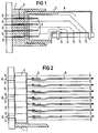
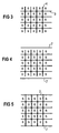
- the exact arrangement of the ground strips 3 or ground platelets 4 in the connector can best be seen in FIGS. 1 and 2, while the meshing is best seen in FIGS. 3 to 7.
- FIG. 1 and in particular 2 shows how a pluggable electrical contact of the ground plate 4 with the pin contacts 5 of the ground strip 3 is made. This contact remains guaranteed over the entire plug area and the service life of the plug.
- the ground plates 4 are preferably connected to the printed circuit board using press-fit technology, sometimes on the edge of the board, sometimes behind the Signal connections to make the unbundling of the signals as difficult as possible.
- the ground strips 3 run over the entire connector length, they are connected at regular intervals to the printed circuit board using press-fit technology, as indicated in FIG. 2. The distance between the connection points 6 is chosen so that the unbundling is disturbed as little as possible and the shielding effect remains optimal.
- the position of the signal contacts is indicated in FIGS. 1 and 2 by "S".
- grounding plates 4 and grounding strips 3 can advantageously be pressed in via the insulating body, so that the pressing tools can be kept as simple as possible.
- ground plates 4 and strips 3 in combination with external shield plates 7, can be operated independently of the shield plates or can also be connected to them. This applies both to two side shield plates, compare FIGS. 4 and 5, and to a 360 ° circumferential shield cage, compare FIGS. 6 and 7.
Landscapes
- Details Of Connecting Devices For Male And Female Coupling (AREA)
- Coupling Device And Connection With Printed Circuit (AREA)
- Connector Housings Or Holding Contact Members (AREA)
Abstract
Description
- Die Erfindung betrifft eine elektrische Verbinderanordnung mit einer Messer- und einer Federleiste aus Isolierstoff, die jeweils eine Mehrzahl von in Spalten und Reihen angeordneten, durch Stecken miteinander verbindbaren Signalkontakten aufweisen, wobei jeder einzelne Signalkontakt durch Blechelemente allseitig geschirmt ist.
- Niederfrequenz-Leiterplattensteckverbinder werden in zunehmendem Maße mit schnelleren digitalen Signalen betrieben. Die sehr steilen Signalanstiegsflanken korrespondieren mit hohen Frequenzen. Dadurch entstehen Probleme mit der Signalübertragungsqualität, insbesondere entstehen zwischen benachbarten Signalkontakten unerwünschte Nebensprecheffekte.
- Konventionell kann das Problem des Nebensprechens dadurch gelöst werden, daß die Signale nur über jeden zweiten Kontakt geführt werden, während die dazwischen liegenden Kontakte mit Masse belegt werden. Bei dieser Lösung ist jedoch die Anzahl der für die Signalübertragung nutzbaren Anschlüsse drastisch verringert, so daß sie für Anwendungen mit einer hohen Signaldichte wenig brauchbar erscheint.
- Aus der DE 40 40 551 C2 ist es bekannt, ein Übersprechen zwischen einander benachbarten Anschlüssen in einander benachbarten vertikalen Reihen durch Einfügen eines Abschirmelements zwischen die vertikalen Anschlußreihen einer Federleiste zu verhindern. Nachteilig bei dieser Lösung ist jedoch, daß von den fünf verfügbaren Kontaktreihen nur drei Reihen für Signale brauchbar sind, und zwei Reihen mit Masse belegt werden. Aus EP 0 486 298 A1 ist andererseits eine Verbinderanordnung bekannt, bei der zwischen den Signalkontakten jeweils um eine halbe Teilung versetzt Massekontakte angeordnet sind, so daß im gesteckten Zustand die Signalkontakte von Massekontakten umgeben sind. Auch diese Lösung ist insofern nicht ideal, als die Einzelkontakte für die Masseführung alle einzeln in die Leiterplatten kontaktiert werden und damit die Entflechtung der Signale erheblich erschweren.
- Aus Markt und Technik - Wochenzeitung für Elektronik, Nr. 26 vom 24. Juni 1994, Seiten 36 bis 37, ist ein Mitglied der 2,5-mm-Steckverbinderfamilie "SIPAC" gemäß dem oben zitierten Oberbegriff des Patentanspruchs 1 bekannt geworden. Dabei erfolgt jedoch eine durchgehende Schirmung jedes einzelnen Kontaktes mit einem dichten metallischen, quadratischen Schacht. Das für diesen Schacht erforderliche "Gefache" von Längs- und Querblechen, die im Abstand von 2,5mm zueinander angeordnet sind, ist vollständig innerhalb der Federleiste angeordnet. An den Durchdringungsstellen der Quer- und Längsbleche müssen deshalb Schlitze vorgesehen werden, die gegenseitig ineinandergreifen und elektrisch hochwertig miteinander kontaktieren.
- Der Erfindung liegt die Aufgabe zugrunde, einen verbesserten
Steckverbinder zu schaffen, der insbesondere als Leiterplattensteckverbinder verwendbar ist, der unerwünschte Nebensprecheffekte verhindert und der einfach herstellbar ist. - Diese Aufgabe wird erfindungsgemäß bei einer Verbinderanordnung der eingangs genannten Art dadurch gelöst,
- a) daß in der Messerleiste über deren gesamte Länge verlaufende Massestreifen vorgesehen und zwischen benachbarten Signalkontaktreihen angeordnet sind,
- b) daß in der Federleiste zwischen benachbarten Signalkontaktspalten Masseplättchen angeordnet sind,
- c) und daß jeder Massestreifen mit stiftförmigen, im Zwischenraster zu den Signalkontakten angeordneten Massekontakten ausgebildet ist, durch die ein steckbarer elektrischer Kontakt mit jedem der Masseplättchen herstellbar ist.
- Weiterbildungen der Erfindung sind Gegenstand von Unteransprüchen.
- Im folgenden wird die Erfindung anhand eines Ausführungsbeispiels und den Figuren der Zeichnung näher erläutert. Es zeigt:
- Figur 1
- eine geschnittene Seitenansicht einer erfindungsgemäßen Verbinderanordnung,
- Figur 2
- die gleiche Verbinderanordnung wie in Figur 1, jedoch in Draufsicht von oben,
- Figuren 3 bis 7
- verschiedene Ausführungen der allseitigen Abschirmung der Signalkontakte durch eine Vermaschung aller Massekontakte, beziehungsweise durch zusätzliche externe Schirmwände.
- Die vorliegende Erfindung bekämpft das Nebensprechen mit Massestreifen und Masseplättchen, die, getrennt nach Messer- und Federleiste, zwischen den Kontaktreihen beziehungsweise den Kontaktspalten liegen. Dadurch entsteht eine Vermaschung aller Massekontakte, mit einer homogenen Schirmwirkung unabhängig von der Kontaktlage im Leiterplatten-Steckverbinder. Die genaue Anordnung der Massestreifen 3 beziehungsweise Masseplättchen 4 im Steckverbinder ergibt sich am besten aus den Figuren 1 und 2, während die Vermaschung am besten aus den Figuren 3 bis 7 erkennbar ist.
- In Figur 1 und insbesondere 2 ist dargestellt, wie ein steckbarer elektrischer Kontakt der Masseplättchen 4 mit den Stiftkontakten 5 der Massestreifen 3 hergestellt ist. Diese Kontaktgabe bleibt über den gesamten Steckbereich und die Lebensdauer des Stecker gewährleistet. Die Masseplättchen 4 werden an der Leiterplatte vorzugsweise in Einpreßtechnik angeschlossen, mal am Leiterplattenrand, mal hinter den Signalanschlüssen, um die Entflechtung der Signale möglichst wenig zu erschweren. Die Massestreifen 3 laufen über die gesamte Steckverbinderlänge, sie werden in regelmäßigen Abständen an der Leiterplatte in Einpreßtechnik, wie in Fig 2 angedeutet, angeschlossen. Der Abstand zwischen den Anschlußpunkten 6 wird so gewählt, daß die Entflechtung möglichst wenig gestört wird und die Schirmwirkung optimal bleibt. Die Position der Signalkontakte ist in den Fig 1 und 2 durch "S" angedeutet.
- Das Einpressen der Masseplättchen 4 und Massestreifen 3 kann vorteilhaft über den Isolierkörper erfolgen, damit die Einpreßwerkzeuge möglichst einfach gehalten werden können. In der Kombination mit externen Schirmblechen 7 können Masseplättchen 4 und Streifen 3 , wie in den Figuren 4 bis 7 dargestellt, unabhängig von den Schirmblechen betrieben oder auch mit diesen verbunden werden. Dies gilt sowohl für zwei seitliche Schirmbleche, vergleiche Figuren 4 und 5, als auch für einen 360° umlaufenden Schirmkäfig, vergleiche Figuren 6 und 7.
Claims (4)
- Elektrische Verbinderanordnung,
mit einer Messer(1)- und einer Federleiste(2) aus Isolierstoff, die jeweils eine Mehrzahl von in Spalten und Reihen angeordneten, durch Stecken miteinander verbindbaren Signalkontakten(S) aufweisen, wobei jeder einzelne Signalkontakt(S) durch Blechelemente allseitig geschirmt ist,
dadurch gekennzeichnet,a) daß in der Messerleiste(1) über deren gesamte Länge verlaufende Massestreifen(3) vorgesehen und zwischen benachbarten Signalkontaktreihen angeordnet sind,b) daß in der Federleiste(2) zwischen benachbarten Signalkontaktspalten Masseplättchen(4) angeordnet sind,c) und daß jeder Massestreifen(3) mit stiftförmigen, im Zwischenraster zu den Signalkontakten(S) angeordneten Massekontakten(5) ausgebildet ist, durch die ein steckbarer elektrischer Kontakt mit jedem der Masseplättchen(4) herstellbar ist. - Verbinderanordnung nach Anspruch 1,
dadurch gekennzeichnet,
daß die Messer(1)- und die Federleiste(2) sowie die Massestreifen(3) und die Masseplättchen(4) in Einpreßtechnik an zwei durch die Verbinderanordnung zu verbindende Leiterplatten angeschlossen sind, wobei die geometrische Anordnung der Masseanschlüsse relativ zu den Signalanschlüssen auf eine Entflechtung der Signale hin optimiert ist. - Verbinderanordnung nach Anspruch 1 oder 2,
dadurch gekennzeichnet,
daß von der Vermaschung der Massekontakte elektrisch unabhängige, zusätzliche externe Schirmbleche(7) vorgesehen sind. - Verbinderanordnung nach Anspruch 1 oder 2,
dadurch gekennzeichnet,
daß zusätzliche externe Schirmbleche(7) vorgesehen sind, die mit der Vermaschung der Massekontakte elektrisch verbunden sind.
Applications Claiming Priority (2)
| Application Number | Priority Date | Filing Date | Title |
|---|---|---|---|
| DE4446100 | 1994-12-22 | ||
| DE4446100 | 1994-12-22 |
Publications (3)
| Publication Number | Publication Date |
|---|---|
| EP0718928A2 true EP0718928A2 (de) | 1996-06-26 |
| EP0718928A3 EP0718928A3 (de) | 1998-03-04 |
| EP0718928B1 EP0718928B1 (de) | 1999-06-16 |
Family
ID=6536788
Family Applications (1)
| Application Number | Title | Priority Date | Filing Date |
|---|---|---|---|
| EP95120165A Expired - Lifetime EP0718928B1 (de) | 1994-12-22 | 1995-12-20 | Elektrische Verbinderanordnung |
Country Status (5)
| Country | Link |
|---|---|
| US (1) | US5632635A (de) |
| EP (1) | EP0718928B1 (de) |
| JP (1) | JPH08236216A (de) |
| AT (1) | ATE181463T1 (de) |
| DE (1) | DE59506232D1 (de) |
Cited By (1)
| Publication number | Priority date | Publication date | Assignee | Title |
|---|---|---|---|---|
| WO2009036865A3 (de) * | 2007-09-17 | 2009-05-07 | Rohde & Schwarz | Steckverbinder mit modifiziertem isolatorkanal zur abschirmung elektromagnetischer strahlung |
Families Citing this family (16)
| Publication number | Priority date | Publication date | Assignee | Title |
|---|---|---|---|---|
| US5876248A (en) * | 1997-01-14 | 1999-03-02 | Molex Incorporated | Matable electrical connectors having signal and power terminals |
| US6494734B1 (en) | 1997-09-30 | 2002-12-17 | Fci Americas Technology, Inc. | High density electrical connector assembly |
| US6231391B1 (en) | 1999-08-12 | 2001-05-15 | Robinson Nugent, Inc. | Connector apparatus |
| DE69929613T2 (de) * | 1998-08-12 | 2006-09-28 | Robinson Nugent, Inc., New Albany | Verbindungsvorrichtung |
| US6471547B1 (en) | 1999-06-01 | 2002-10-29 | John T. Venaleck | Electrical connector for high density signal interconnections and method of making the same |
| NL1013740C2 (nl) * | 1999-12-03 | 2001-06-06 | Fci S Hertogenbosch B V | Afgeschermde connector. |
| AU2001271371A1 (en) | 2000-06-29 | 2002-01-14 | Robinson Nugent, Inc. | High speed connector |
| US6428358B1 (en) * | 2000-12-28 | 2002-08-06 | Intel Corporation | Socket with embedded conductive structure and method of fabrication therefor |
| US6612857B2 (en) | 2001-07-05 | 2003-09-02 | Bernard R. Tolmie | Electrical connector system and method having optical and/or cooling capability |
| US6821146B2 (en) * | 2002-01-07 | 2004-11-23 | Bernard R. Tolmie | Hybrid connector system and method |
| JP2004087348A (ja) | 2002-08-28 | 2004-03-18 | Fujitsu Component Ltd | コネクタ装置 |
| WO2005053102A2 (en) * | 2003-11-21 | 2005-06-09 | Ohio Associated Enterprises Llc | Cable assembly and method of making |
| US7484989B2 (en) * | 2006-11-29 | 2009-02-03 | Ohio Associated Enterprises, Llc | Low friction cable assembly latch |
| US8475177B2 (en) * | 2010-01-20 | 2013-07-02 | Ohio Associated Enterprises, Llc | Backplane cable interconnection |
| US9281630B2 (en) * | 2014-07-11 | 2016-03-08 | Tyco Electronics Corporation | Electrical connector systems |
| KR102312443B1 (ko) * | 2018-06-12 | 2021-10-12 | 주식회사 엘지에너지솔루션 | 서지 방지 기능을 가진 커넥터 및 이를 포함하는 회로기판 |
Citations (2)
| Publication number | Priority date | Publication date | Assignee | Title |
|---|---|---|---|---|
| EP0486298A1 (de) | 1990-11-15 | 1992-05-20 | The Whitaker Corporation | Mehrpoliger Verbinder zur Signalübertragung |
| DE4040551C2 (de) | 1989-12-20 | 1993-04-29 | Amp Inc., Harrisburg, Pa., Us |
Family Cites Families (6)
| Publication number | Priority date | Publication date | Assignee | Title |
|---|---|---|---|---|
| US4571014A (en) * | 1984-05-02 | 1986-02-18 | At&T Bell Laboratories | High frequency modular connector |
| US4611867A (en) * | 1985-07-08 | 1986-09-16 | Japan Aviation Electronics Industry Limited | Coaxial multicore receptacle |
| NL9000578A (nl) * | 1990-03-14 | 1991-10-01 | Burndy Electra Nv | Connectorsamenstel voor printkaarten. |
| GB9205088D0 (en) * | 1992-03-09 | 1992-04-22 | Amp Holland | Shielded back plane connector |
| DE4313771C2 (de) * | 1993-04-27 | 1996-09-19 | Rudolf Goerlich | Steckverbinder für Leiterplatten |
| NL9300971A (nl) * | 1993-06-04 | 1995-01-02 | Framatome Connectors Belgium | Connectorsamenstel voor printkaarten. |
-
1995
- 1995-12-20 DE DE59506232T patent/DE59506232D1/de not_active Expired - Fee Related
- 1995-12-20 AT AT95120165T patent/ATE181463T1/de not_active IP Right Cessation
- 1995-12-20 EP EP95120165A patent/EP0718928B1/de not_active Expired - Lifetime
- 1995-12-22 JP JP7350188A patent/JPH08236216A/ja not_active Withdrawn
- 1995-12-22 US US08/577,563 patent/US5632635A/en not_active Expired - Fee Related
Patent Citations (2)
| Publication number | Priority date | Publication date | Assignee | Title |
|---|---|---|---|---|
| DE4040551C2 (de) | 1989-12-20 | 1993-04-29 | Amp Inc., Harrisburg, Pa., Us | |
| EP0486298A1 (de) | 1990-11-15 | 1992-05-20 | The Whitaker Corporation | Mehrpoliger Verbinder zur Signalübertragung |
Non-Patent Citations (1)
| Title |
|---|
| MARKT UND TECHNIK - WOCHENZEITUNG FUER ELEKTRONIK, no. 26, 24 June 1994 (1994-06-24), pages 36 - 37 |
Cited By (2)
| Publication number | Priority date | Publication date | Assignee | Title |
|---|---|---|---|---|
| WO2009036865A3 (de) * | 2007-09-17 | 2009-05-07 | Rohde & Schwarz | Steckverbinder mit modifiziertem isolatorkanal zur abschirmung elektromagnetischer strahlung |
| US7980866B2 (en) | 2007-09-17 | 2011-07-19 | Rohde & Schwarz Gmbh & Co. Kg | Plug-in connector comprising a modified insulator duct for shielding electromagnetic radiation |
Also Published As
| Publication number | Publication date |
|---|---|
| EP0718928A3 (de) | 1998-03-04 |
| JPH08236216A (ja) | 1996-09-13 |
| DE59506232D1 (de) | 1999-07-22 |
| ATE181463T1 (de) | 1999-07-15 |
| US5632635A (en) | 1997-05-27 |
| EP0718928B1 (de) | 1999-06-16 |
Similar Documents
| Publication | Publication Date | Title |
|---|---|---|
| EP0871998B1 (de) | Elektrischer verbinder mit abschirmung | |
| DE60314228T2 (de) | Verbinderanordnung für l-förmige erdungsabschirmungen und differentialkontaktpaare | |
| DE69711716T2 (de) | Verbinderanordnung mit abgeschirmten modulen und verfahren für seine herstellung | |
| DE10392455B4 (de) | Verbindungsleiste für elektrischen Verbinder | |
| DE69103652T2 (de) | Verbinderanordnung für gedruckte Leiterplatten. | |
| DE69112658T2 (de) | Abgeschirmter Verbinder. | |
| DE3750105T2 (de) | Elektrische Steckverbinder. | |
| EP0674363B1 (de) | Vielpoliger Steckverbinder mit Filteranordnung | |
| DE69212725T2 (de) | Verbinder mit Erdungsanordnung | |
| EP0718928B1 (de) | Elektrische Verbinderanordnung | |
| DE69309309T2 (de) | Verbindungssystem | |
| EP2476165B1 (de) | Steckverbindung mit abschirmung | |
| DE69116806T2 (de) | Mehrpoliger Verbinder zur Signalübertragung | |
| DE69827347T2 (de) | Mehrpolige elektrische Steckverbindung | |
| DE69123881T2 (de) | Steckverbinder mit Erdungsstruktur | |
| EP0670615A1 (de) | Steckverbinder für Rückwandverdrahtungen | |
| DE4040551A1 (de) | Elektrische verbinderanordnung | |
| EP0735624A2 (de) | Elektrischer Verbinder | |
| DE2845632A1 (de) | Elektrisches verbindungselement | |
| DE68918547T2 (de) | Elektrisches Verbindersystem. | |
| DE19614788A1 (de) | Anschlußleiste für hohe Übertragungsraten | |
| DE69331910T2 (de) | Ein verbinder mit verbesserter abschirmung | |
| EP0556200B1 (de) | Vielpoliger geschirmter steckverbinder | |
| EP0582960A1 (de) | HF-Koaxial-Steckverbindung | |
| EP1535372B1 (de) | Elektrische steckbuchse |
Legal Events
| Date | Code | Title | Description |
|---|---|---|---|
| PUAI | Public reference made under article 153(3) epc to a published international application that has entered the european phase |
Free format text: ORIGINAL CODE: 0009012 |
|
| AK | Designated contracting states |
Kind code of ref document: A2 Designated state(s): AT BE CH DE FR GB IT LI SE |
|
| PUAL | Search report despatched |
Free format text: ORIGINAL CODE: 0009013 |
|
| AK | Designated contracting states |
Kind code of ref document: A3 Designated state(s): AT BE CH DE FR GB IT LI SE |
|
| 17P | Request for examination filed |
Effective date: 19980805 |
|
| GRAG | Despatch of communication of intention to grant |
Free format text: ORIGINAL CODE: EPIDOS AGRA |
|
| GRAG | Despatch of communication of intention to grant |
Free format text: ORIGINAL CODE: EPIDOS AGRA |
|
| GRAH | Despatch of communication of intention to grant a patent |
Free format text: ORIGINAL CODE: EPIDOS IGRA |
|
| 17Q | First examination report despatched |
Effective date: 19981202 |
|
| GRAH | Despatch of communication of intention to grant a patent |
Free format text: ORIGINAL CODE: EPIDOS IGRA |
|
| GRAA | (expected) grant |
Free format text: ORIGINAL CODE: 0009210 |
|
| AK | Designated contracting states |
Kind code of ref document: B1 Designated state(s): AT BE CH DE FR GB IT LI SE |
|
| REF | Corresponds to: |
Ref document number: 181463 Country of ref document: AT Date of ref document: 19990715 Kind code of ref document: T |
|
| REG | Reference to a national code |
Ref country code: CH Ref legal event code: NV Representative=s name: SIEMENS SCHWEIZ AG Ref country code: CH Ref legal event code: EP |
|
| REF | Corresponds to: |
Ref document number: 59506232 Country of ref document: DE Date of ref document: 19990722 |
|
| ET | Fr: translation filed | ||
| ITF | It: translation for a ep patent filed | ||
| GBT | Gb: translation of ep patent filed (gb section 77(6)(a)/1977) |
Effective date: 19990819 |
|
| PLBE | No opposition filed within time limit |
Free format text: ORIGINAL CODE: 0009261 |
|
| STAA | Information on the status of an ep patent application or granted ep patent |
Free format text: STATUS: NO OPPOSITION FILED WITHIN TIME LIMIT |
|
| 26N | No opposition filed | ||
| REG | Reference to a national code |
Ref country code: CH Ref legal event code: PUE Owner name: SIEMENS AKTIENGESELLSCHAFT TRANSFER- TYCO ELECTRON Ref country code: CH Ref legal event code: NV Representative=s name: RIEDERER HASLER & PARTNER PATENTANWAELTE AG |
|
| REG | Reference to a national code |
Ref country code: CH Ref legal event code: AEN Free format text: DAS PATENT IST AUFGRUND DES WEITERBEHANDLUNGSANTRAGS VOM 27.07.2000 REAKTIVIERT WORDEN. |
|
| PGFP | Annual fee paid to national office [announced via postgrant information from national office to epo] |
Ref country code: AT Payment date: 20001103 Year of fee payment: 6 |
|
| PGFP | Annual fee paid to national office [announced via postgrant information from national office to epo] |
Ref country code: SE Payment date: 20001201 Year of fee payment: 6 |
|
| PGFP | Annual fee paid to national office [announced via postgrant information from national office to epo] |
Ref country code: CH Payment date: 20010103 Year of fee payment: 6 |
|
| REG | Reference to a national code |
Ref country code: GB Ref legal event code: 732E |
|
| PGFP | Annual fee paid to national office [announced via postgrant information from national office to epo] |
Ref country code: BE Payment date: 20010118 Year of fee payment: 6 |
|
| PGFP | Annual fee paid to national office [announced via postgrant information from national office to epo] |
Ref country code: GB Payment date: 20011102 Year of fee payment: 7 |
|
| PGFP | Annual fee paid to national office [announced via postgrant information from national office to epo] |
Ref country code: FR Payment date: 20011203 Year of fee payment: 7 |
|
| PG25 | Lapsed in a contracting state [announced via postgrant information from national office to epo] |
Ref country code: AT Free format text: LAPSE BECAUSE OF NON-PAYMENT OF DUE FEES Effective date: 20011220 |
|
| PG25 | Lapsed in a contracting state [announced via postgrant information from national office to epo] |
Ref country code: SE Free format text: LAPSE BECAUSE OF NON-PAYMENT OF DUE FEES Effective date: 20011221 |
|
| PG25 | Lapsed in a contracting state [announced via postgrant information from national office to epo] |
Ref country code: LI Free format text: LAPSE BECAUSE OF NON-PAYMENT OF DUE FEES Effective date: 20011231 Ref country code: CH Free format text: LAPSE BECAUSE OF NON-PAYMENT OF DUE FEES Effective date: 20011231 Ref country code: BE Free format text: LAPSE BECAUSE OF NON-PAYMENT OF DUE FEES Effective date: 20011231 |
|
| REG | Reference to a national code |
Ref country code: GB Ref legal event code: IF02 |
|
| BERE | Be: lapsed |
Owner name: SIEMENS A.G. Effective date: 20011231 |
|
| EUG | Se: european patent has lapsed |
Ref document number: 95120165.6 |
|
| REG | Reference to a national code |
Ref country code: CH Ref legal event code: PL |
|
| PG25 | Lapsed in a contracting state [announced via postgrant information from national office to epo] |
Ref country code: GB Free format text: LAPSE BECAUSE OF NON-PAYMENT OF DUE FEES Effective date: 20021220 |
|
| GBPC | Gb: european patent ceased through non-payment of renewal fee |
Effective date: 20021220 |
|
| PG25 | Lapsed in a contracting state [announced via postgrant information from national office to epo] |
Ref country code: FR Free format text: LAPSE BECAUSE OF NON-PAYMENT OF DUE FEES Effective date: 20030901 |
|
| REG | Reference to a national code |
Ref country code: FR Ref legal event code: ST |
|
| PG25 | Lapsed in a contracting state [announced via postgrant information from national office to epo] |
Ref country code: IT Free format text: LAPSE BECAUSE OF NON-PAYMENT OF DUE FEES;WARNING: LAPSES OF ITALIAN PATENTS WITH EFFECTIVE DATE BEFORE 2007 MAY HAVE OCCURRED AT ANY TIME BEFORE 2007. THE CORRECT EFFECTIVE DATE MAY BE DIFFERENT FROM THE ONE RECORDED. Effective date: 20051220 |
|
| PGFP | Annual fee paid to national office [announced via postgrant information from national office to epo] |
Ref country code: DE Payment date: 20080131 Year of fee payment: 13 |
|
| PG25 | Lapsed in a contracting state [announced via postgrant information from national office to epo] |
Ref country code: DE Free format text: LAPSE BECAUSE OF NON-PAYMENT OF DUE FEES Effective date: 20090701 |