EP0719004A2 - OFDM-System mit zusätzlichem Schutz gegen Mehrpfadeffekte - Google Patents
OFDM-System mit zusätzlichem Schutz gegen Mehrpfadeffekte Download PDFInfo
- Publication number
- EP0719004A2 EP0719004A2 EP95119990A EP95119990A EP0719004A2 EP 0719004 A2 EP0719004 A2 EP 0719004A2 EP 95119990 A EP95119990 A EP 95119990A EP 95119990 A EP95119990 A EP 95119990A EP 0719004 A2 EP0719004 A2 EP 0719004A2
- Authority
- EP
- European Patent Office
- Prior art keywords
- complex
- signal group
- symbol
- signal
- division multiplex
- Prior art date
- Legal status (The legal status is an assumption and is not a legal conclusion. Google has not performed a legal analysis and makes no representation as to the accuracy of the status listed.)
- Granted
Links
Images







Classifications
-
- H—ELECTRICITY
- H04—ELECTRIC COMMUNICATION TECHNIQUE
- H04L—TRANSMISSION OF DIGITAL INFORMATION, e.g. TELEGRAPHIC COMMUNICATION
- H04L27/00—Modulated-carrier systems
- H04L27/26—Systems using multi-frequency codes
- H04L27/2601—Multicarrier modulation systems
- H04L27/2602—Signal structure
- H04L27/2605—Symbol extensions, e.g. Zero Tail, Unique Word [UW]
- H04L27/2607—Cyclic extensions
-
- H—ELECTRICITY
- H04—ELECTRIC COMMUNICATION TECHNIQUE
- H04L—TRANSMISSION OF DIGITAL INFORMATION, e.g. TELEGRAPHIC COMMUNICATION
- H04L27/00—Modulated-carrier systems
- H04L27/26—Systems using multi-frequency codes
- H04L27/2601—Multicarrier modulation systems
- H04L27/2614—Peak power aspects
Definitions
- the present invention relates to an orthogonal frequency division multiplexing (hereinafter referred to as OFDM) transmission method, and more specifically, it relates to a method of transmitting data between a transmission side and a receiving side through a wire or wireless transmission path with an orthogonal frequency division multiplex signal including symbols of prescribed lengths and guard intervals of prescribed lengths which are arranged between the symbols.
- OFDM orthogonal frequency division multiplexing
- an OFDM transmission system is adapted to divide coded data and sort the same into at least hundreds of carriers, for multiplexing and transmitting the data.
- communication through an OFDM signal is recently watched with interest.
- the OFDM signal can transmit a large quantity of data at a high speed while its characteristics are hardly deteriorated by reflected waves even if no waveform equalizer is provided. Further, this signal hardly causes a crossfire to another service since its signal waveform is close to that of a random noise.
- a transmission system employing such an OFDM signal is disclosed in "Suitable for Mobile Receiving of OFDM Digital Broadcasting Employing at least Hundreds of Carriers” by Hajime Fukuchi of the Communications Research Laboratory, the Ministry of Posts and Telecommunications of Japan, “Data Compression and Digital Modulation", Nikkei Electronics Books, issued on October 1, 1993, pp. 207 to 222.
- Fig. 13 is a block circuit diagram showing the structure of a conventional transmitter 5 for an OFDM signal which is disclosed in the aforementioned literature
- Fig. 14 illustrates the structure of an OFDM signal which is transmitted from the transmitter 5 shown in Fig. 13.
- the transmitter 5 comprises a serial-to-parallel converter 52, an inverse Fourier transformer 53, a parallel-to-serial converter 54, a digital-to-analog converter 55, and a low-pass filter 56.
- (a), (b) and (c) show direct, reflected and composite waves of the OFDM signal respectively, and (d) shows a time window W.
- the serial-to-parallel converter 52 of the transmitter 5 is supplied with an input symbol train.
- the input symbol train is formed by digitally modulated transmission data, and each transmission symbol includes a plurality of data values.
- the digital modulation is performed by QPSK (quadriphase phase shift keying) modulation or 16 QAM (quadrature amplitude modulation).
- the serial-to-parallel converter 52 serial-to-parallel converts the input symbol train in every symbol, to obtain a plurality of symbol trains of a lower speed.
- the degree of parallelism is identical to the number (such as 512, for example, in the range of tens to thousands) of a plurality of carriers, which are orthogonal in phase to each other, employed in the inverse Fourier transformer 53. Due to this operation, the serial-to-parallel converter 52 outputs a group of carrier modulation signals for deciding the amplitudes and phases of the plurality of carriers which are employed in the inverse Fourier transformer 53.
- the inverse Fourier transformer 53 allots the carrier modulation signals to the respective carriers which are lined up on the frequency axis in every symbol so that data for one symbol is transformed to a multiplex signal on the frequency axis, and collectively performs inverse Fourier transformation on the signals, thereby transforming the same to a multiplex signal (parallel digital signal in this stage) on the time axis.
- the parallel-to-serial converter 54 parallel-to-serial converts the multiplex signal on the time axis, thereby forming a OFDM signal.
- the digital-to-analog converter 55 converts the OFDM signal to an analog OFDM baseband signal.
- the low-pass filter 56 limits the band of the OFDM baseband signal, so that no channel-to-channel interference is caused by aliasing.
- the transmitter 5 outputs the OFDM signal including guard intervals Gm and symbols Sm to the transmission path, as shown in Fig. 14.
- a demodulator (not shown) carries out signal processing which is reverse to that of the modulator 5 on the OFDM signal received through the transmission path, to reproduce an output symbol train which is identical to the input symbol train.
- the so-called multipath is caused on the transmission path. Therefore, the receiver receives direct waves of the OFDM signal transmitted from the transmitter and reflected waves which are time-delayed from the direct waves in superposition. If a reflected wave (see (b) in Fig. 14) by the multipath is superposed on a direct wave (see (a) in Fig. 14) in the symbol Sm, for example, an interference part am with the guard interval Gm of the reflected wave is caused on a front end part of the symbol Sm of a composite wave (see (c) in Fig. 14), while an interference part ⁇ m with a symbol Sm-1 of the reflected wave is caused on a front end part of the guard interval Gm.
- the interference part ⁇ m which is displaced from the time window W exerts no influence on Fourier transformation of the symbol Sm.
- the interference part ⁇ m is caused in the time window W while the data component of the guard interval Gm is "0", and hence waveform distortion is disadvantageously caused on the data component of each symbol Sm on the frequency axis after the Fourier transformation.
- the carrier modulation signals which are outputted from the serial-to-parallel converter 52 may not be out of phase with each other, but may be completely in phase with each other.
- the carrier modulation signals are completely in phase with each other when a silent state is transmitted in excess of one symbol period in digital sound broadcasting or when a monochromatic picture is transmitted in excess of one symbol period in terrestrial digital television broadcasting.
- the carrier modulation signals tend to be completely in phase with each other in a digital modulation system such as the QPSK modulation or the 16 QAM, due to a limited number of signal points which are out of phase with each other.
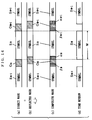
- a group of n carrier modulation signals for modulating n carriers which are orthogonal to each other respectively are completely in phase with each other on a complex plane.
- the n carriers which are modulated by the n carrier modulation signals shown in Fig. 15(a) are multiplexed on the time axis.
- the OFDM signal becomes an impulsive waveform signal.
- a group of n carrier modulation signals for modulating n carriers which are orthogonal to each other respectively are at random in phase on a complex plane. Referring to Fig.
- the n carriers which are modulated by the n carrier modulation signals shown in Fig. 15(c) are multiplexed on the time axis.
- the OFDM signal is enenly diffused on the time axis, and becomes a random waveform signal.
- the OFDM signal has an impulsive waveform to extremely increase the maximum power when the carrier modulation signals are completely in phase with each other, and hence the OFDM signal is disadvantageously readily influenced by nonlinearity of the transmitter, the receiver, a relay amplifier such as a satellite or a CATV included in the transmission path and the like.
- the dynamic ranges of the transmitter, the receiver, the relay amplifier and the like may be increased to exert no influences of nonlinearity on the impulsive OFDM signal, while the cost for the transmitter, the receiver, the relay amplifier and the like is disadvantageously increased in this case.
- an object of the present invention is to provide a method of transmitting an OFDM signal which causes no waveform distortion in a data component of each symbol on the frequency axis after Fourier transformation even if a reflected wave is superposed on a direct wave through a multipath, and a transmitter and a receiver therefor.
- Another object of the present invention is to provide a method of transmitting an OFDM signal which can readily adjust a time window on the time axis even if a time delay is caused in the OFDM signal before the same reaches a receiving side from a transmission side, and a transmitter and a receiver therefor.
- Still another object of the present invention is to provide a method of transmitting an OFDM signal which can reduce an influence of nonlinearity on the OFDM signal in a low-priced structure, and a transmitter and a receiver therefor.
- a first aspect of the present invention is directed to a method of transmitting an orthogonal frequency division multiplex signal in every symbol of a prescribed length from a transmission side to a receiving side through a wire or wireless transmission path, and the method comprises: a first step of transforming a carrier modulation signal group deciding the phases and amplitudes of a plurality of carriers which are orthogonal to each other on the frequency axis to the orthogonal frequency division multiplex signal on the time axis by performing inverse Fourier transformation in every symbol; and a second step of adding front and rear guard intervals, including data which are identical to those of rear and front end parts of each symbol of the orthogonal frequency division multiplex signal, to front and rear parts of the symbol respectively and transmitting the same to the receiving side.
- the front and rear guard intervals including the data which are identical to those of parts of each symbol are added to the front and rear parts of the symbol in transmission of each symbol of the OFDM signal, whereby all data components in a single symbol interval which are lined up on the time axis can be reproduced on the receiving side even if a time window in the Fourier transformation is slightly displaced from the symbol interval of the received signal. Therefore, it is not necessary to correctly coincide the time window with the symbol interval even if a time delay is caused in the OFDM signal before the same reaches the receiving side from the transmission side, whereby the time window can be readily adjusted on the time axis.
- the carrier modulation signal group is complex-multiplied by a reference complex signal group on the frequency axis, so that the complex multiplication result is transformed to an OFDM signal and transmitted to the receiving side.
- the OFDM signal which is transmitted from the transmission side is transformed to a receiving carrier modulation signal group so that this receiving carrier modulation signal group is complex-divided by the reference complex signal group on the frequency axis. Even if a time delay is caused in the OFDM signal between the transmission side and the receiving side, therefore, modulated data can be obtained on the receiving side with no influence by the time delay.
- a result of complex multiplication which is carried out in advance of a constant symbol may be employed with respect to each symbol of the carrier modulation signal group.
- the reference complex signal group may be prepared from a complex signal group having a predetermined specific pattern with signals which vary in phase at random.
- a complex multiplication result which is obtained in a third step is ordinarily transformed to an OFDM signal, while the reference complex signal group is periodically transformed to an OFDM signal.
- the absolute reference phases of the respective signals of the carrier modulation signal group are random values, whereby the OFDM signal obtained by the inverse Fourier transformation can be suppressed from time concentration of power.
- a second aspect of the present invention is directed to a transmitter for an orthogonal frequency division multiplex signal, which is an apparatus for transmitting the orthogonal frequency division multiplex signal to a receiving side in every symbol of a prescribed length through a wire or wireless transmission path, and the transmitter comprises: a memory part storing a reference complex signal group; a complex multiplication part, complex-multiplying a carrier modulation signal group deciding the phases and amplitudes of a plurality of carriers which are orthogonal to each other on the frequency axis, by the reference complex signal group stored in the memory part on the frequency axis, for outputting a transmission carrier modulation signal group; an inverse Fourier transformation part performing an inverse Fourier operation on the transmission carrier modulation signal group which is outputted from the complex multiplication part in every symbol thereby transforming the transmission carrier modulation signal group to the orthogonal frequency division multiplex signal on the time axis; a guard interval addition part adding front and rear guard intervals, including data which are identical to those of rear and front end parts of each symbol
- the memory part stores a complex multiplication result of the complex multiplication part which is precedent to a constant symbol as the reference complex signal group.
- the memory part stores a predetermined complex signal group as the reference complex signal group.
- the complex multiplication part complex-multiplies the carrier modulation signal group by the reference complex signal group which is stored in the memory part on the frequency axis and outputs the result.
- the inverse Fourier transformation part ordinarily transforms the complex multiplication result which is outputted from the complex multiplication part to an orthogonal frequency division multiplex signal in every symbol, and periodically transforms the reference complex signal group which is outputted from the memory part to an orthogonal frequency division multiplex signal.
- the memory part may hold an output of a pseudo-noise signal generation part generating a pseudo-noise signal or that of a frequency sweep signal generation part generating a frequency sweep signal as the reference complex signal group.
- a third aspect of the present invention is directed to a receiver for an orthogonal frequency division multiplex signal, which is an apparatus for receiving the orthogonal frequency division multiplex signal transmitted from a transmission side in every symbol of a prescribed length through a wire or wireless transmission path, and the receiver comprises: a Fourier transformation part performing a Fourier transformation operation on the orthogonal frequency division multiplex signal on the time axis in every symbol thereby transforming the orthogonal frequency division multiplex signal to a receiving carrier modulation signal group on the frequency axis; a memory part storing the receiving carrier modulation signal group which is outputted from the Fourier transformation part in every symbol as a receiving reference complex signal group; and a complex division part complex-dividing the receiving carrier modulation signal group which is outputted from the Fourier transformation part by the receiving reference complex signal group which is stored in the memory part on the frequency axis.
- a fourth aspect of the present invention is directed to a method of transmitting an orthogonal frequency division multiplex signal from a transmission side to a receiving side in every symbol of a prescribed length through a wire or wireless transmission path, and the method comprises: a first step of forming a carrier modulation signal group for deciding the phases and amplitudes of a plurality of carriers which are orthogonal to each other on the frequency axis in every symbol; a second step of generating a complex signal group having a predetermined specific pattern with signals varying in phase at random; a third step of complex-multiplying the carrier modulation signal group by the complex signal group on the frequency axis in every symbol, thereby randomizing phases of respective signals of the carrier modulation signal group; and a fourth step of ordinarily transforming the carrier modulation signal group having the signals which are randomized in phase in the third step to an orthogonal frequency division multiplex signal on the time axis by inverse Fourier transformation in every symbol, and periodically transforming the complex signal group to an orthogonal frequency division multiple
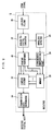
- Fig. 1 is a block diagram showing a transmitter 1 according to a first embodiment of the present invention
- Fig. 2 is a block diagram showing the structure of a receiver 2 according to the first embodiment of the present invention
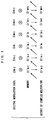
- Fig. 3 illustrates an exemplary structure of an OFDM signal which is employed in the present invention.
- (a) and (b) show direct and reflected waves of the OFDM signal respectively
- (c) and (d) show direct and reflected waves of the OFDM signal causing time delays respectively
- (e) shows a time window W.
- the transmitter 1 shown in Fig. 1 and the receiver 2 shown in Fig. 2 are connected with each other through a transmission path (not shown) such as a coaxial cable or an optical fiber cable.
- the transmitter 1 and the receiver 2 are employed in a digital CATV system, for example.
- the transmitter 1 is adapted to transmit picture data for multiple channels of a television, for example, to the receiver 2 through an OFDM signal.
- the transmitter 1 comprises a carrier modulation signal generator 12, a complex multiplier 13, a memory 14, an inverse Fourier transformer 15, a guard interval insertion part 16, a synchronizing signal multiplexing part 17, a digital-to-analog converter 18, and a low-pass filter 19.
- the carrier modulation signal generator 12 of the transmitter 1 receives transmitted digital data (bit stream signal) to be transmitted to the receiver 2.
- the carrier modulation signal generator 12 digital-modulates the inputted transmitted digital data and serial-to-parallel converts the same in every symbol interval, thereby converting the data to a carrier modulation signal group including n (512, for example, in the range of tens to thousands) carrier modulation signals for modulating n carriers which are orthogonal to each other.
- the digital modulation is performed by QPSK modulation or 16 QAM.
- the carrier modulation signal group in this stage is similar to that outputted from the serial-to-parallel converter 52 (see Fig. 13) of the conventional transmitter.
- the carrier modulation signal group which is outputted from the carrier modulation signal generator 12 is supplied to the complex multiplier 13.
- the memory 14 can store such a carrier modulation signal group D'm outputted from the complex multiplier 13 for one symbol.
- a carrier modulation signal group Dm is inputted in the complex multiplier 13
- the memory 14 outputs a carrier modulation signal group D'm-1, which is precedent to one symbol, stored therein to the complex multiplier 13 as a prescribed reference complex signal group.
- the inverse Fourier transformer 15 successively allots the respective carrier modulation signals included in the carrier modulation signal group D'm which is outputted from the complex multiplier 13 to the respective carriers which are lined up on the frequency axis in every symbol interval, collectively performs inverse Fourier transformation thereon, and further performs parallel-to-serial conversion, thereby transforming the carrier modulation signal group multiplexed with the respective data components on the frequency axis to an OFDM signal D'mt multiplexed with the respective data components on the time axis.
- the guard interval insertion part 16 temporarily stores the digital OFDM signal D'mt which is outputted from the inverse Fourier transformer 15 in its internal buffer in every symbol interval. Then, the guard interval insertion circuit 16 adds front and rear guard intervals Ghm and Gem to front and rear parts of each symbol Sm (see Fig. 3). Time lengths tg1 and tg2 of the front and rear guard intervals Ghm and Gem are prescribed in consideration of time difference between direct and indirect waves due to a multipath caused in the transmission path and time delays resulting from sampling deviation between the digital-to-analog converter 18 of the transmitter 1 and an analog-to-digital converter 22 of the receiver 2.
- the front and rear guard intervals Ghm and Gem include data D'emt and D'hmt which are identical to those of rear and front end parts Sem and Shm of the corresponding symbol Sm respectively.
- the substantial symbol length is extended to tg1 + ts + tg2 .
- the guard interval insertion part 16 successively outputs the data D'emt, D'm and D'hmt through the front guard interval Ghm, the symbol Sm and the rear guard interval Gem.
- the synchronizing signal multiplexing part 17 multiplexes a synchronizing signal on the OFDM signal to which the guard intervals are added on the time axis in every symbol in order to indicate the breakpoint of the symbol, and outputs the signal to the digital-to-analog converter 18.
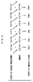
- the synchronizing signal is formed by a periodically known nonmodulated carrier, a suppression signal etc. with respect to the OFDM signal, as shown at (a) in Fig. 5, for example.
- the digital-to-analog converter 18 converts the OFDM signal of the digital data, to which the guard intervals and the synchronizing signal are added, outputted from the synchronizing signal multiplexing part 17 to an analog OFDM baseband signal.
- the low-pass filter 19 limits the band of the OFDM baseband signal, so that no channel-to-channel interference is caused by aliasing.
- the transmitter 1 outputs the OFDM signal including the guard intervals and the synchronizing signal to the transmission path.
- the receiver 2 comprises a low-pass filter 21, the analog-to-digital converter 22, an envelope detector 23, a synchronous reproducing part 24, a Fourier transformer 25, a memory 26, a complex divider 27, and a transmission data reproducer 28.
- the low-pass filter 21 removes unnecessary spectral components of a high-frequency region from the OFDM signal which is received through the transmission path.
- the analog-to-digital converter 22 converts data ZD'emt, ZD'mt and ZD'hmt which are included in the front guard interval Ghm, the symbol Sm and the rear guard interval Gem of the analog OFDM signal respectively to those of a digital OFDM signal.
- the envelope detector 23 envelope-detects the OFDM signal, thereby outputting an envelope detection signal shown at (b) in Fig. 5 in every symbol.
- the synchronous reproducing part 24 outputs a reference timing signal shown at (c) in Fig. 5 in every symbol on the basis of the envelope detection signal outputted from the envelope detector 23. This reference timing signal is inputted in the Fourier transformer 25 and the memory 26.
- the Fourier transformer 25 observes the OFDM signal which is outputted from the analog-to-digital converter 22 in synchronization with the reference timing signal through the time window W (see (e) in Fig. 3) of the same length as the symbol length ts, thereby extracting only necessary data parts of the respective symbols.
- the Fourier transformer 25 further performs Fourier transformation operations on the extracted data parts, thereby transforming the OFDM signal on the time axis to a receiving carrier modulation signal group on the frequency axis.
- the memory 26 stores the receiving carrier modulation signal group which is outputted from the Fourier transformer 25 for one symbol.
- the memory 26 stores data ZD'm as corresponding data.
- the memory 26 outputs the data ZD'm to the complex divider 27 in synchronization with the reference timing signal.
- the complex divider 27 establishes synchronization, and then complex-divides data ZD'm+1 of a symbol Sm+1 which is outputted from the Fourier transformer 25 by the data ZD'm held in the memory 26.
- a relative time delay is caused between the direct and reflected waves shown at (a) and (b) in Fig. 3, due to the multipath.
- specific time delays are caused in the direct and reflected waves, due to the difference in sampling timing between the digital-to-analog converter 18 of the transmitter 1 and the analog-to-digital converter 22 of the receiver 2 (see (c) and (d) in Fig. 3).
- These time delays are not taken into consideration in the Fourier transformer 25 as to the reference timing signal, and hence positions of the receiving side time window W on the time axis are displaced from the symbol intervals of the received signal, as shown at (e) in Fig. 3.
- the time window W is displaced from correct symbol intervals in the Fourier transformer 25 of the receiving side, however, the data observed through the time window W include all data ZD'mt on the time axis which must be originally included in one symbol interval since the front and rear guard intervals Ghm and Gem include the data ZD'emt and ZD'hmt respectively. Therefore, the time delays and superposition of the reflected waves appear as uniform amplitude/phase distortion in every data component on the frequency axis. When the time delays and the characteristics of the reflected waves are uniform, the values of the amplitude/phase distortion in the respective symbol intervals are equal to each other.
- the guard intervals including the data which are identical to those of the front and rear end parts of each symbol are added to the front and rear parts of the symbol respectively for transmitting the data, whereby all data components in one symbol interval which are lined up on the time axis can be reproduced on the receiving side as to both of the direct and reflected waves in the time window W. Therefore, the respective data components appearing on the frequency axis after the Fourier transformation are uniform in amplitude/phase distortion even if the reflected waves are superposed on the direct waves by the multipath to result in superposition of the symbol intervals of the direct waves and the guard intervals of the reflected waves. Therefore, waveform distortion can be readily removed from the receiving carrier modulation signal group on the frequency axis of one symbol interval by executing proper operations (multiplication and division) on the transmission and receiving sides.
- demodulated data can be obtained with no time delay even if a time delay is caused in the OFDM signal between the transmission and receiving sides, by complex-multiplying and complex-dividing the receiving carrier modulation signal group by the prescribed reference complex signal group on the frequency axis. Consequently, it is not necessary to correctly coincide the time window with the symbol interval.
- the transmission data reproducer 28 demaps signal points of the receiving carrier modulation signal group Dm which is outputted from the complex divider 27 on a complex plane and decides the signal points, thereby obtaining a receiving digital signal group which is identical in value to the transmission digital signal group of the transmitter 1. As hereinabove described, phase distortion and amplitude distortion are removed from the receiving carrier modulation signal group Dm. Therefore, the transmission data reproducer 28 can correctly and readily determine the original data from the mapping positions on the complex plane.
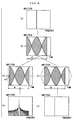
- the inventors have made simulations of comparing the system according to this embodiment with the conventional system with respect to influences exerted by waves delayed by multipaths and those exerted by time axis delays respectively through a calculator. Each simulation was executed on such conditions that the carrier number was 512, only data of a 256-th carrier had an amplitude "1" and a phase "0", and all data of the remaining carriers were "0".
- Fig. 7 illustrates the results of the simulation for comparing the system according to this embodiment with the conventional system as to the influences exerted by waves delayed by multipaths.
- (a), (b), (c) and (d) show data distortion states in the case of transforming direct, indirect, composite and composite waves in the conventional system to signals on the frequency axis by Fourier operations respectively.
- (e), (f), (g) and (h) show data distortion states in the case of converting direct, indirect, composite and composite waves in the system according to this embodiment to signals on the frequency axis by Fourier operations respectively.
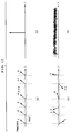
- Fig. 8 illustrates the results of the simulation for comparing the system according to this embodiment with the conventional system as to the influences exerted by time delays caused by transmission paths etc.
- (a) shows a spectrum obtained under such conditions that only the data of the 256-th carrier had an amplitude "1" and a phase "0”
- (b) shows a signal waveform in the case of transforming the data at (a) to a signal on the time axis by an inverse Fourier operation.
- (c) and (d) show data distortion states in the case of transforming composite and composite waves causing time delays in the conventional system to signals on the frequency axis by Fourier operations respectively.
- (e) and (f) show data distortion states in the case of transforming composite and composite waves causing time delays in the system according to this embodiment to signals on the frequency axis by Fourier operations respectively.
- Fig. 9 is a block diagram showing the structure of a transmitter 3 according to a second embodiment of the present invention.
- a memory 14 holds an output of a specific pattern generator 31, i.e., a complex signal group D0 having a predetermined specific pattern with signals which mutually vary in phase at random.
- Such a complex signal group D0 can be formed by a pseudo-noise signal generator comprising a PN series pseudo-random signal generator for generating a pseudo-random signal which is at a level between zero and 1 and a multiplier for multiplying the pseudo-random signal by 2 ⁇ for generating a unit vector signal in a phase having a random value in the range of zero to 2 ⁇ and an amplitude of 1, for example.
- the complex signal group D0 can be formed by a frequency sweep signal generator for generating a known frequency sweep signal in a phase having a random value in the range of zero to 2 ⁇ .
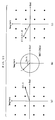
- Fig. 10 illustrates a complex multiplication operation in the complex multiplier 13.
- (a) in Fig. 10 shows arrangement of signal points which can be taken by the carrier modulation signals when 16 QAM is employed as a modulation system,
- (b) shows a unit vector i whose phase varies at random, and
- (c) shows a carrier modulation signal whose phase is randomized to a specific pattern.
- a carrier modulation signal included in a carrier modulation signal group which is allotted to one carrier is arranged at a signal point A on a complex plane.
- the signal A has a real number part of 3 and an imaginary number part of 1. It is also assumed that the unit vector i has a phase angle of 3 ⁇ /4 at this time.
- a carrier modulation signal A' shown at (c) in Fig. 10 is obtained as the result of a complex multiplication.
- the carrier modulation signal A' has a real number part of - 2.8 and an imaginary number part of 1.4, and takes a signal point which is not present in the arrangement of the 16 QAM.
- the phase of the unit vector i varies at random, and hence the complex multiplier 13 outputs a carrier modulation signal group having signals whose phases are mutually randomized to an inverse Fourier transformer 15 even if respective carrier modulation signals included in a carrier modulation signal group which is outputted from a carrier modulation signal generator 12 are in phase with each other.
- the complex multiplier 13 repeats such an operation for a prescribed period. Further, the complex multiplier 13 periodically outputs only the data D0.
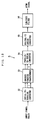
- Fig. 11 shows a series of such operations. Assuming that S0 represents a symbol in which the data D0 is inserted, the transmitter 3 periodically outputs the data D0 of the symbol S0 while outputting data Dm of a symbol Sm in other case, as shown in Fig. 12.
- the inverse Fourier transformer 15 allots the carrier modulation signal group D'm to respective carriers which are lined up on the frequency axis in every symbol, and collectively performs inverse Fourier transformation and parallel-to-serial conversion thereon, thereby converting the same to a digital OFDM signal.
- absolute reference phases of the carrier modulation signal group are at random values in the range of zero to 2 ⁇ whereby the OFDM signal outputted from the inverse Fourier transformer 15 can be suppressed from power concentration.
- the remaining circuit blocks in the transmitter 3, i.e., those from a guard interval insertion part 16 to a low-pass filter 19, operate similarly to those in the transmitter 1.
- the guard interval insertion part 16 inserts a data component D0 which is identical to that of a rear end part of the symbol S0 in a corresponding front guard interval, while inserting a data component which is identical to that of a front end part of the symbol S0 in a corresponding rear guard interval, similarly to the case of the symbol Sm.
- a receiver of the same structure as the receiver 2 shown in Fig. 2 can basically be employed.
- a memory 26 of the receiver stores receiving data ZD0 of a reference complex signal group D0 which is stored in the memory 14 of the transmitter 3.
- amplitude/phase distortion of a receiving carrier modulation signal group appearing on the frequency axis after Fourier transformation is entirely uniform even if reflected waves are superposed on direct waves by a multipath and symbol intervals of the direct waves are superposed with guard intervals of the reflected waves, and can be removed by simple operations (multiplication and division).
- demodulated data can be obtained with no influence by a time delay even if such a time delay is caused in the OFDM signal between the transmission and receiving sides, whereby a time window can be readily adjusted on the time axis.
- the present invention is not restricted to this but data may alternatively be transmitted through a wireless transmission path.
- television picture data for multichannels are carried on the respective carriers in the aforementioned embodiments
- picture data for one channel may alternatively be time-shared and sequenced in a parallel manner, to be allotted to respective carriers.
- voice data, text data or the like may be carried on the respective carriers, in place of the picture data.
- the present invention may alternatively be carried out in another system such as LAN or WAN, in place of the CATV.
- the reference complex signal group outputted from the memory 14 is periodically inputted in the inverse Fourier transformer 15 through the complex multiplier 13 in the transmitter 3 shown in Fig. 9, the reference complex signal group may alternatively be directly inputted in the inverse Fourier transformer 15.
- the transmitter 3 shown in Fig. 9 employs the complex signal group D0 including signals having a predetermined specific pattern and phases which mutually vary at random as the reference complex signal group to be included in the carrier modulation signal group
- the reference complex signal group to be included in the carrier modulation signal group may alternatively be formed by a complex signal group including signals having a predetermined specific pattern which are in phase with each other under a situation causing no power concentration in the OFDM signal.
- amplitude/phase distortion can be removed by simple operations (multiplication and division), similarly to the first embodiment.
Landscapes
- Engineering & Computer Science (AREA)
- Computer Networks & Wireless Communication (AREA)
- Signal Processing (AREA)
- Digital Transmission Methods That Use Modulated Carrier Waves (AREA)
- Detection And Prevention Of Errors In Transmission (AREA)
- Noise Elimination (AREA)
Applications Claiming Priority (6)
| Application Number | Priority Date | Filing Date | Title |
|---|---|---|---|
| JP31690094 | 1994-12-20 | ||
| JP31690094 | 1994-12-20 | ||
| JP316900/94 | 1994-12-20 | ||
| JP6073295 | 1995-03-20 | ||
| JP6073295 | 1995-03-20 | ||
| JP60732/95 | 1995-03-20 |
Publications (3)
| Publication Number | Publication Date |
|---|---|
| EP0719004A2 true EP0719004A2 (de) | 1996-06-26 |
| EP0719004A3 EP0719004A3 (de) | 1999-12-01 |
| EP0719004B1 EP0719004B1 (de) | 2011-06-22 |
Family
ID=26401782
Family Applications (1)
| Application Number | Title | Priority Date | Filing Date |
|---|---|---|---|
| EP95119990A Expired - Lifetime EP0719004B1 (de) | 1994-12-20 | 1995-12-18 | OFDM-System mit zusätzlichem Schutz gegen Mehrpfadeffekte |
Country Status (2)
| Country | Link |
|---|---|
| US (1) | US5682376A (de) |
| EP (1) | EP0719004B1 (de) |
Cited By (16)
| Publication number | Priority date | Publication date | Assignee | Title |
|---|---|---|---|---|
| EP0863644A3 (de) * | 1997-03-04 | 2000-01-05 | AT&T Corp. | Mehrton DPSK-Modem auf FFT-Basis |
| DE19858106A1 (de) * | 1998-12-16 | 2000-06-29 | Ericsson Telefon Ab L M | Empfänger und Verfahren zum Verhindern einer Zwischensymbolstörung in einem Hochgeschwindigkeitsübertragungssystem |
| FR2788907A1 (fr) * | 1999-01-27 | 2000-07-28 | St Microelectronics Sa | Generation d'intervalle de garde dans une transmission en modulation dmt |
| EP0859494A3 (de) * | 1997-02-17 | 2000-08-23 | Matsushita Electric Industrial Co., Ltd. | Synchronisierung vom lokalen Oszillator, in Mehrträgersystem |
| EP1065855A1 (de) * | 1999-06-29 | 2001-01-03 | Sony International (Europe) GmbH | Anpassung der Schutzintervalle in einem OFDM-Kommunikationssystem |
| EP0851641A3 (de) * | 1996-12-26 | 2001-03-21 | Sony Corporation | Kommunikationsverfahren und Empfangsvorrichtung für OFDM-Systeme |
| EP0851638A3 (de) * | 1996-12-26 | 2001-03-21 | Sony Corporation | Empfangsverfahren und Empfangsgerät für OFDM-System |
| AT408396B (de) * | 1998-12-21 | 2001-11-26 | Ericsson Austria Ag | Verfahren zur übertragung von daten |
| WO2001035591A3 (en) * | 1999-11-09 | 2002-01-17 | Aware Inc | Par reduction by carriers phase randomization in multicarrier communications |
| GB2385756A (en) * | 2002-01-24 | 2003-08-27 | Lg Electronics Inc | FFT window position recovery system utilising first and second guard interv inserted into divided symbols |
| US6961369B1 (en) | 1999-11-09 | 2005-11-01 | Aware, Inc. | System and method for scrambling the phase of the carriers in a multicarrier communications system |
| WO2006109868A1 (en) * | 2005-04-08 | 2006-10-19 | Matsushita Electric Industrial Co., Ltd. | Communication apparatus and communication method thereof |
| WO2007042900A1 (en) * | 2005-10-14 | 2007-04-19 | Nokia Corporation | Phase noise canceling ofdm receiver |
| CN100384114C (zh) * | 1998-12-22 | 2008-04-23 | 松下电器产业株式会社 | 正交频分复用通信装置及方法 |
| GB2515854A (en) * | 2013-07-04 | 2015-01-07 | Sony Corp | Transmitter and receiver and methods of transmitting and receiving |
| CN110047503A (zh) * | 2018-09-25 | 2019-07-23 | 上海无线通信研究中心 | 一种声波的多径效应抑制方法及装置 |
Families Citing this family (54)
| Publication number | Priority date | Publication date | Assignee | Title |
|---|---|---|---|---|
| US5774450A (en) * | 1995-01-10 | 1998-06-30 | Matsushita Electric Industrial Co., Ltd. | Method of transmitting orthogonal frequency division multiplexing signal and receiver thereof |
| EP0790722B1 (de) * | 1996-02-16 | 2003-12-03 | STMicroelectronics S.r.l. | Automatische Detektion des Übertragungsmodus in Empfängern von digitalen Tonsignalen |
| US6678311B2 (en) | 1996-05-28 | 2004-01-13 | Qualcomm Incorporated | High data CDMA wireless communication system using variable sized channel codes |
| CA2183140C (en) * | 1996-08-12 | 2001-11-20 | Telecommunications Research Laboratories | Ofdm timing and frequency recovery system |
| US5995483A (en) | 1996-08-22 | 1999-11-30 | Tellabs Operations, Inc. | Apparatus and method for upstream clock synchronization in a multi-point OFDM/DMT digital communication system |
| US6285654B1 (en) * | 1996-08-22 | 2001-09-04 | Tellabs Operations, Inc. | Apparatus and method for symbol alignment in a multi-point OFDM or DMT digital communications system |
| US6122246A (en) * | 1996-08-22 | 2000-09-19 | Tellabs Operations, Inc. | Apparatus and method for clock synchronization in a multi-point OFDM/DMT digital communications system |
| US6771590B1 (en) | 1996-08-22 | 2004-08-03 | Tellabs Operations, Inc. | Communication system clock synchronization techniques |
| US6118758A (en) | 1996-08-22 | 2000-09-12 | Tellabs Operations, Inc. | Multi-point OFDM/DMT digital communications system including remote service unit with improved transmitter architecture |
| US6950388B2 (en) * | 1996-08-22 | 2005-09-27 | Tellabs Operations, Inc. | Apparatus and method for symbol alignment in a multi-point OFDM/DMT digital communications system |
| FR2754125B1 (fr) * | 1996-09-30 | 2004-07-09 | Sc Reprosol | Dispositif et procede d'egalisation vectorielle d'un signal ofdm |
| KR100221336B1 (ko) * | 1996-12-28 | 1999-09-15 | 전주범 | 직교 주파수 분할 다중화 수신 시스템의 프레임 동기 장치 및 그 방법 |
| KR100226698B1 (ko) * | 1996-12-28 | 1999-10-15 | 전주범 | 직교 주파수 분할 다중화 수신 시스템의 채널 등화 장치 |
| FI102340B (fi) * | 1997-01-16 | 1998-11-13 | Nokia Telecommunications Oy | Tiedonsiirtomenetelmä ja radiojärjestelmä |
| CN1207865C (zh) * | 1997-03-26 | 2005-06-22 | 西门子公司 | 经移动通信系统的无线电接口发送用户信号的数据符的方法和发送设备 |
| CA2258935A1 (en) * | 1997-04-30 | 1998-11-05 | Sony Corporation | Device and method for transmitting digital data |
| US6151296A (en) * | 1997-06-19 | 2000-11-21 | Qualcomm Incorporated | Bit interleaving for orthogonal frequency division multiplexing in the transmission of digital signals |
| JPH11163807A (ja) * | 1997-09-29 | 1999-06-18 | Matsushita Electric Ind Co Ltd | 通信システム、送信器および受信器 |
| EP0929172B1 (de) | 1998-01-06 | 2010-06-02 | MOSAID Technologies Inc. | System zur Mehrträgermodulation, mit veränderbaren Symbolgeschwindigkeiten |
| US6546055B1 (en) * | 1998-01-12 | 2003-04-08 | The Board Of Trustees Of The Leland Stanford Junior University | Carrier offset determination for RF signals having a cyclic prefix |
| DE19802398C1 (de) * | 1998-01-22 | 1999-05-06 | Siemens Ag | Verfahren zur Verarbeitung eines Signals aus Datensymbolen |
| US6631175B2 (en) | 1998-04-03 | 2003-10-07 | Tellabs Operations, Inc. | Spectrally constrained impulse shortening filter for a discrete multi-tone receiver |
| DK1068704T3 (da) | 1998-04-03 | 2012-09-17 | Tellabs Operations Inc | Filter til impulssvarforkortning, med yderligere spektrale begrænsninger, til multibærebølgeoverførsel |
| US7440498B2 (en) | 2002-12-17 | 2008-10-21 | Tellabs Operations, Inc. | Time domain equalization for discrete multi-tone systems |
| KR100314353B1 (ko) * | 1998-04-28 | 2001-12-28 | 전주범 | 직교분할대역수신시스템 |
| JP4066523B2 (ja) * | 1998-07-22 | 2008-03-26 | ソニー株式会社 | Ofdm信号発生方法及びofdm信号発生装置 |
| US6111919A (en) * | 1999-01-20 | 2000-08-29 | Intellon Corporation | Synchronization of OFDM signals |
| US6442130B1 (en) * | 1999-01-21 | 2002-08-27 | Cisco Technology, Inc. | System for interference cancellation |
| US6539063B1 (en) | 1999-02-18 | 2003-03-25 | Ibiquity Digital Corporation | System and method for recovering symbol timing offset and carrier frequency error in an OFDM digital audio broadcast system |
| DE60028276T2 (de) * | 1999-03-26 | 2007-05-03 | Nec Corp. | Verringerung von Verzögerung in Mehrträgerempfängern |
| US6356528B1 (en) | 1999-04-15 | 2002-03-12 | Qualcomm Incorporated | Interleaver and deinterleaver for use in a diversity transmission communication system |
| US6269132B1 (en) | 1999-04-26 | 2001-07-31 | Intellon Corporation | Windowing function for maintaining orthogonality of channels in the reception of OFDM symbols |
| US6074086A (en) * | 1999-04-26 | 2000-06-13 | Intellon Corporation | Synchronization of OFDM signals with improved windowing |
| US6859504B1 (en) | 1999-06-29 | 2005-02-22 | Sharp Laboratories Of America, Inc. | Rapid settling automatic gain control with minimal signal distortion |
| US6505037B1 (en) * | 1999-06-29 | 2003-01-07 | Sharp Laboratories Of America, Inc. | Data unit detection including antenna diversity |
| US6529868B1 (en) | 2000-03-28 | 2003-03-04 | Tellabs Operations, Inc. | Communication system noise cancellation power signal calculation techniques |
| US6975585B1 (en) | 2000-07-27 | 2005-12-13 | Conexant Systems, Inc. | Slotted synchronous frequency division multiplexing for multi-drop networks |
| DE60037583T2 (de) * | 2000-08-24 | 2009-01-08 | Sony Deutschland Gmbh | Kommunikationseinrichtung zum Senden und Empfangen von OFDM Signalen in einem Funkkommunikationssystem |
| US7020095B2 (en) * | 2001-06-16 | 2006-03-28 | Maxim Integrated Products, Inc. | System and method for modulation of non-data bearing carriers in a multi-carrier modulation system |
| US7170961B2 (en) * | 2002-01-08 | 2007-01-30 | Patrick Vandenameele-Lepla | Method and apparatus for frequency-domain tracking of residual frequency and channel estimation offsets |
| KR100824369B1 (ko) * | 2002-05-28 | 2008-04-22 | 삼성전자주식회사 | 오에프디엠 송신기 및 그의 ofdm 심볼에 보호구간삽입방법 |
| KR100859866B1 (ko) * | 2002-05-30 | 2008-09-24 | 삼성전자주식회사 | 디지털 방송신호의 전송효율을 향상시킬 수 있는오에프디엠송신기 및 그의 신호처리방법 |
| KR100884402B1 (ko) * | 2002-06-20 | 2009-02-17 | 삼성전자주식회사 | 데이터의 영역 별 수신 우선 순위에 따라 상이한 개수의파일럿 톤을 삽입하는 디지털방송 송신기 |
| EP1553714B1 (de) | 2002-07-16 | 2020-07-01 | Optis Wireless Technology, LLC | Kommunikationsverfahren und übertragungsgerät |
| KR20070061215A (ko) * | 2005-12-08 | 2007-06-13 | 한국전자통신연구원 | 다중 반송파를 이용한 광대역 무선 채널 측정 장치의송수신 장치 |
| WO2007066949A2 (en) * | 2005-12-08 | 2007-06-14 | Electronics And Telecommunications Research Institute | Transmitting/receiving apparatus of wideband wireless channel apparatus using multiple carriers |
| US7907673B2 (en) * | 2006-10-26 | 2011-03-15 | Telefonaktiebolaget L M Ericsson (Publ) | Robust and low-complexity combined signal power estimation |
| US7929624B2 (en) * | 2006-10-26 | 2011-04-19 | Telefonaktiebolaget L M Ericsson (Publ) | Cell ID detection in cellular communication systems |
| US8730933B2 (en) * | 2008-09-18 | 2014-05-20 | Qualcomm Incorporated | Method and apparatus for multiplexing data and reference signal in a wireless communication system |
| TWI382683B (zh) * | 2009-05-06 | 2013-01-11 | Ind Tech Res Inst | 預補償光纖色散所引起的延遲的方法、應用該方法的多子載波訊號產生器、以及應用該訊號產生器的光正交分頻多工系統之傳送器 |
| US9288026B2 (en) * | 2009-06-22 | 2016-03-15 | Qualcomm Incorporated | Transmission of reference signal on non-contiguous clusters of resources |
| JP2011014982A (ja) * | 2009-06-30 | 2011-01-20 | Fujitsu Ltd | 無線受信装置 |
| US9831933B1 (en) | 2016-08-10 | 2017-11-28 | The United States Of America As Represented By Secretary Of The Navy | Techniques and methods for frequency division multiplexed digital beamforming |
| US9998304B1 (en) * | 2017-06-06 | 2018-06-12 | Trellisware Technologies, Inc. | Methods and systems for estimating and mitigating OFDM interference |
Family Cites Families (11)
| Publication number | Priority date | Publication date | Assignee | Title |
|---|---|---|---|---|
| GB9020170D0 (en) * | 1990-09-14 | 1990-10-24 | Indep Broadcasting Authority | Orthogonal frequency division multiplexing |
| JP2904986B2 (ja) * | 1992-01-31 | 1999-06-14 | 日本放送協会 | 直交周波数分割多重ディジタル信号送信装置および受信装置 |
| DE69322322T2 (de) * | 1992-07-08 | 1999-06-17 | Koninklijke Philips Electronics N.V., Eindhoven | Verkettete Kodierung für OFDM-Übertragung |
| FR2693861A1 (fr) * | 1992-07-16 | 1994-01-21 | Philips Electronique Lab | Récepteur de signaux à répartition multiplexée de fréquences orthogonales muni d'un dispositif de synchronisation de fréquences. |
| FR2701178A1 (fr) * | 1993-02-03 | 1994-08-05 | Philips Electronique Lab | Système de communication par étalement de spectre à multiutilisateurs. |
| CA2115118A1 (en) * | 1993-02-08 | 1994-08-09 | Arie Geert Cornelis Koppelaar | Method of transmitting a data stream, transmitter and receiver |
| US5371548A (en) * | 1993-07-09 | 1994-12-06 | Cable Television Laboratories, Inc. | System for transmission of digital data using orthogonal frequency division multiplexing |
| EP0660559B1 (de) * | 1993-12-22 | 2005-04-27 | Koninklijke Philips Electronics N.V. | Mehrträger-Frequenzsprungkommunikationssystem |
| SE501608C2 (sv) * | 1994-01-18 | 1995-03-27 | Telia Ab | Förfarande och arrangemang för synkronisering vid OFDM- modulering |
| GB9413481D0 (en) * | 1994-07-05 | 1994-08-24 | British Broadcasting Corp | Improvements to digital transmission systems |
| JP3577754B2 (ja) * | 1994-09-09 | 2004-10-13 | ソニー株式会社 | 通信方法及び装置 |
-
1995
- 1995-12-14 US US08/572,719 patent/US5682376A/en not_active Expired - Lifetime
- 1995-12-18 EP EP95119990A patent/EP0719004B1/de not_active Expired - Lifetime
Non-Patent Citations (1)
| Title |
|---|
| None |
Cited By (38)
| Publication number | Priority date | Publication date | Assignee | Title |
|---|---|---|---|---|
| EP0851638A3 (de) * | 1996-12-26 | 2001-03-21 | Sony Corporation | Empfangsverfahren und Empfangsgerät für OFDM-System |
| EP0851641A3 (de) * | 1996-12-26 | 2001-03-21 | Sony Corporation | Kommunikationsverfahren und Empfangsvorrichtung für OFDM-Systeme |
| EP0859494A3 (de) * | 1997-02-17 | 2000-08-23 | Matsushita Electric Industrial Co., Ltd. | Synchronisierung vom lokalen Oszillator, in Mehrträgersystem |
| US6148024A (en) * | 1997-03-04 | 2000-11-14 | At&T Corporation | FFT-based multitone DPSK modem |
| EP0863644A3 (de) * | 1997-03-04 | 2000-01-05 | AT&T Corp. | Mehrton DPSK-Modem auf FFT-Basis |
| DE19858106A1 (de) * | 1998-12-16 | 2000-06-29 | Ericsson Telefon Ab L M | Empfänger und Verfahren zum Verhindern einer Zwischensymbolstörung in einem Hochgeschwindigkeitsübertragungssystem |
| DE19858106B4 (de) * | 1998-12-16 | 2014-09-25 | Telefonaktiebolaget Lm Ericsson (Publ) | Empfänger und Verfahren zum Verhindern einer Zwischensymbolstörung in einem Hochgeschwindigkeitsübertragungssystem |
| US6870893B2 (en) | 1998-12-16 | 2005-03-22 | Telefonaktiebolaget Lm Ericsson | Receiver and method for avoiding intersymbol interference in a high speed transmission system |
| AT408396B (de) * | 1998-12-21 | 2001-11-26 | Ericsson Austria Ag | Verfahren zur übertragung von daten |
| CN100384114C (zh) * | 1998-12-22 | 2008-04-23 | 松下电器产业株式会社 | 正交频分复用通信装置及方法 |
| EP1024635A1 (de) * | 1999-01-27 | 2000-08-02 | STMicroelectronics S.A. | Schutzintervallerzeugung in einer Übertragung mit DMT-Modulation |
| FR2788907A1 (fr) * | 1999-01-27 | 2000-07-28 | St Microelectronics Sa | Generation d'intervalle de garde dans une transmission en modulation dmt |
| EP1065855A1 (de) * | 1999-06-29 | 2001-01-03 | Sony International (Europe) GmbH | Anpassung der Schutzintervalle in einem OFDM-Kommunikationssystem |
| US7471721B2 (en) | 1999-11-09 | 2008-12-30 | Aware, Inc. | System and method for scrambling the phase of the carriers in a multicarrier communications system |
| US8718158B2 (en) | 1999-11-09 | 2014-05-06 | Tq Delta, Llc | System and method for scrambling the phase of the carriers in a multicarrier communications system |
| US9755876B2 (en) | 1999-11-09 | 2017-09-05 | Tq Delta, Llc | System and method for scrambling the phase of the carriers in a multicarrier communications system |
| US8929470B2 (en) | 1999-11-09 | 2015-01-06 | Tq Delta, Llc | System and method for scrambling the phase of the carriers in a multicarrier communications system |
| US7292627B2 (en) | 1999-11-09 | 2007-11-06 | Aware, Inc. | System and method for scrambling the phase of the carriers in a multicarrier communications system |
| WO2001035591A3 (en) * | 1999-11-09 | 2002-01-17 | Aware Inc | Par reduction by carriers phase randomization in multicarrier communications |
| US9014243B2 (en) | 1999-11-09 | 2015-04-21 | Tq Delta, Llc | System and method for scrambling using a bit scrambler and a phase scrambler |
| US10187240B2 (en) | 1999-11-09 | 2019-01-22 | Tq Delta, Llc | System and method for scrambling the phase of the carriers in a multicarrier communications system |
| US7769104B2 (en) | 1999-11-09 | 2010-08-03 | Aware, Inc. | System and method for scrambling the phase of the carriers in a multicarrier communications system |
| US8073041B1 (en) | 1999-11-09 | 2011-12-06 | Aware, Inc. | System and method for descrambling the phase of the carriers in a multicarrier communications system |
| US8090008B2 (en) | 1999-11-09 | 2012-01-03 | Aware, Inc. | System and method for scrambling the phase of the carriers in a multicarrier communications system |
| US8218610B2 (en) | 1999-11-09 | 2012-07-10 | Aware, Inc. | System and method for descrambling the phase of carriers in a multicarrier communications system |
| US8355427B2 (en) | 1999-11-09 | 2013-01-15 | Tq Delta, Llc | System and method for descrambling the phase of carriers in a multicarrier communications system |
| US6961369B1 (en) | 1999-11-09 | 2005-11-01 | Aware, Inc. | System and method for scrambling the phase of the carriers in a multicarrier communications system |
| GB2385756A (en) * | 2002-01-24 | 2003-08-27 | Lg Electronics Inc | FFT window position recovery system utilising first and second guard interv inserted into divided symbols |
| GB2385756B (en) * | 2002-01-24 | 2004-09-22 | Lg Electronics Inc | FFT window position recovery system and method |
| WO2006109868A1 (en) * | 2005-04-08 | 2006-10-19 | Matsushita Electric Industrial Co., Ltd. | Communication apparatus and communication method thereof |
| WO2007042900A1 (en) * | 2005-10-14 | 2007-04-19 | Nokia Corporation | Phase noise canceling ofdm receiver |
| US7733993B2 (en) | 2005-10-14 | 2010-06-08 | Nokia Corporation | Phase noise canceling OFDM receiver |
| GB2515861A (en) * | 2013-07-04 | 2015-01-07 | Sony Corp | Transmitter and receiver and methods of transmitting and receiving |
| GB2515854A (en) * | 2013-07-04 | 2015-01-07 | Sony Corp | Transmitter and receiver and methods of transmitting and receiving |
| US10404507B2 (en) | 2013-07-04 | 2019-09-03 | Sony Corporation | Implicit signaling in OFDM preamble with embedded signature sequence, and cyclic prefix and postfix aided signature detection |
| US10999111B2 (en) | 2013-07-04 | 2021-05-04 | Saturn Licensing Llc | Implicit signalling in OFDM preamble with embedded signature sequence, and cyclic prefix and postfix aided signature detection |
| US11496345B2 (en) | 2013-07-04 | 2022-11-08 | Saturn Licensing Llc | Implicit signaling in OFDM preamble with embedded signature sequence, and cyclic prefix and postfix aided signature detection |
| CN110047503A (zh) * | 2018-09-25 | 2019-07-23 | 上海无线通信研究中心 | 一种声波的多径效应抑制方法及装置 |
Also Published As
| Publication number | Publication date |
|---|---|
| US5682376A (en) | 1997-10-28 |
| EP0719004A3 (de) | 1999-12-01 |
| EP0719004B1 (de) | 2011-06-22 |
Similar Documents
| Publication | Publication Date | Title |
|---|---|---|
| US5682376A (en) | Method of transmitting orthogonal frequency division multiplex signal, and transmitter and receiver employed therefor | |
| US7020218B2 (en) | Sliding-window transform with integrated windowing | |
| EP1183774B1 (de) | Synchronisation von ofdm signalen mit verbesserter fensterfunktion | |
| AU660965B2 (en) | System for broadcasting and receiving digital data, receiver and transmitter for use in such system | |
| US7394848B2 (en) | Method and apparatus for time equalization | |
| JP3539522B2 (ja) | 直交周波数分割多重信号の伝送方法ならびにその送信装置および受信装置 | |
| EP0839423B1 (de) | Pulsformung für mehrträgermodulation | |
| KR960007813B1 (ko) | 직각 진폭 변조 동기화 방법 | |
| US7058140B2 (en) | Sliding-window multi-carrier frequency division multiplexing system | |
| US4300161A (en) | Time compression multiplexing of video signals | |
| EP1181797B1 (de) | Eine fensterungsfunktion zur erhaltung von orthogonalität beim empfang von ofdm-symbolen | |
| US5416767A (en) | Method of transmitting a data stream, transmitter and receiver | |
| US6151372A (en) | Diversity receiver | |
| JP2001094524A (ja) | 通信システム、送信装置、受信装置、送信方法、受信方法、および、情報記録媒体 | |
| US6058145A (en) | Method of demodulating a multi-frequency quadrature modulated signal | |
| US5144641A (en) | Spread spectrum communication device | |
| EP0993161A2 (de) | Mehrträgerübertragung zweier Datenmengen | |
| TW200412044A (en) | Communication apparatus | |
| GB2291314A (en) | Coding an orthogonal frequency division multiplexed (OFDM) signal | |
| KR20000074899A (ko) | 주파수도약/직교주파수분할다중방식 통신시스템 | |
| EP0613267A2 (de) | OFDM-System mit Verringerung des Übersprechens | |
| US5220584A (en) | System for demodulation and synchronizing multiple tone waveforms | |
| JP3592783B2 (ja) | 伝送路等化器 | |
| KR100195748B1 (ko) | 직교 주파수 분할 다중 수신 시스템 | |
| JP3514965B2 (ja) | 受信装置 |
Legal Events
| Date | Code | Title | Description |
|---|---|---|---|
| PUAI | Public reference made under article 153(3) epc to a published international application that has entered the european phase |
Free format text: ORIGINAL CODE: 0009012 |
|
| AK | Designated contracting states |
Kind code of ref document: A2 Designated state(s): DE FR GB NL SE |
|
| RIC1 | Information provided on ipc code assigned before grant |
Free format text: 6H 04L 5/06 A, 6H 04L 27/26 B |
|
| PUAL | Search report despatched |
Free format text: ORIGINAL CODE: 0009013 |
|
| AK | Designated contracting states |
Kind code of ref document: A3 Designated state(s): DE FR GB NL SE |
|
| 17P | Request for examination filed |
Effective date: 20000120 |
|
| RAP1 | Party data changed (applicant data changed or rights of an application transferred) |
Owner name: PANASONIC CORPORATION |
|
| GRAP | Despatch of communication of intention to grant a patent |
Free format text: ORIGINAL CODE: EPIDOSNIGR1 |
|
| GRAS | Grant fee paid |
Free format text: ORIGINAL CODE: EPIDOSNIGR3 |
|
| GRAA | (expected) grant |
Free format text: ORIGINAL CODE: 0009210 |
|
| AK | Designated contracting states |
Kind code of ref document: B1 Designated state(s): DE FR GB NL SE |
|
| REG | Reference to a national code |
Ref country code: GB Ref legal event code: FG4D |
|
| REG | Reference to a national code |
Ref country code: DE Ref legal event code: R096 Ref document number: 69536173 Country of ref document: DE Effective date: 20110728 |
|
| REG | Reference to a national code |
Ref country code: SE Ref legal event code: TRGR |
|
| REG | Reference to a national code |
Ref country code: NL Ref legal event code: T3 |
|
| PLBE | No opposition filed within time limit |
Free format text: ORIGINAL CODE: 0009261 |
|
| STAA | Information on the status of an ep patent application or granted ep patent |
Free format text: STATUS: NO OPPOSITION FILED WITHIN TIME LIMIT |
|
| 26N | No opposition filed |
Effective date: 20120323 |
|
| REG | Reference to a national code |
Ref country code: DE Ref legal event code: R097 Ref document number: 69536173 Country of ref document: DE Effective date: 20120323 |
|
| REG | Reference to a national code |
Ref country code: DE Ref legal event code: R082 Ref document number: 69536173 Country of ref document: DE Representative=s name: BARDEHLE PAGENBERG PARTNERSCHAFT PATENTANWAELT, DE |
|
| REG | Reference to a national code |
Ref country code: DE Ref legal event code: R082 Ref document number: 69536173 Country of ref document: DE Representative=s name: BARDEHLE PAGENBERG PARTNERSCHAFT MBB PATENTANW, DE Effective date: 20130826 Ref country code: DE Ref legal event code: R082 Ref document number: 69536173 Country of ref document: DE Representative=s name: BARDEHLE PAGENBERG PARTNERSCHAFT PATENTANWAELT, DE Effective date: 20130826 Ref country code: DE Ref legal event code: R081 Ref document number: 69536173 Country of ref document: DE Owner name: PANASONIC INTELLECTUAL PROPERTY CORPORATION OF, US Free format text: FORMER OWNER: PANASONIC CORPORATION, KADOMA, OSAKA, JP Effective date: 20130826 Ref country code: DE Ref legal event code: R081 Ref document number: 69536173 Country of ref document: DE Owner name: PANASONIC INTELLECTUAL PROPERTY CORPORATION OF, US Free format text: FORMER OWNER: MATSUSHITA ELECTRIC INDUSTRIAL CO., LTD., KADOMA-SHI, OSAKA, JP Effective date: 20110608 Ref country code: DE Ref legal event code: R081 Ref document number: 69536173 Country of ref document: DE Owner name: HARRIS CORPORATION (N. D. GES. D. STAATES DELA, US Free format text: FORMER OWNER: PANASONIC CORPORATION, KADOMA, OSAKA, JP Effective date: 20130826 Ref country code: DE Ref legal event code: R081 Ref document number: 69536173 Country of ref document: DE Owner name: HARRIS CORPORATION (N. D. GES. D. STAATES DELA, US Free format text: FORMER OWNER: MATSUSHITA ELECTRIC INDUSTRIAL CO., LTD., KADOMA-SHI, OSAKA, JP Effective date: 20110608 Ref country code: DE Ref legal event code: R081 Ref document number: 69536173 Country of ref document: DE Owner name: HARRIS CORPORATION (N. D. GES. D. STAATES DELA, US Free format text: FORMER OWNER: MATSUSHITA ELECTRIC INDUSTRIAL CO., LTD., KADOMA-SHI, JP Effective date: 20110608 Ref country code: DE Ref legal event code: R081 Ref document number: 69536173 Country of ref document: DE Owner name: HARRIS CORPORATION (N. D. GES. D. STAATES DELA, US Free format text: FORMER OWNER: PANASONIC CORPORATION, KADOMA, JP Effective date: 20130826 |
|
| REG | Reference to a national code |
Ref country code: GB Ref legal event code: 732E Free format text: REGISTERED BETWEEN 20130926 AND 20131002 |
|
| REG | Reference to a national code |
Ref country code: FR Ref legal event code: TP Owner name: HARRIS CORPORATION, US Effective date: 20130927 |
|
| REG | Reference to a national code |
Ref country code: NL Ref legal event code: SD Effective date: 20141002 |
|
| PGFP | Annual fee paid to national office [announced via postgrant information from national office to epo] |
Ref country code: GB Payment date: 20141229 Year of fee payment: 20 |
|
| PGFP | Annual fee paid to national office [announced via postgrant information from national office to epo] |
Ref country code: NL Payment date: 20141226 Year of fee payment: 20 Ref country code: FR Payment date: 20141217 Year of fee payment: 20 |
|
| PGFP | Annual fee paid to national office [announced via postgrant information from national office to epo] |
Ref country code: DE Payment date: 20141230 Year of fee payment: 20 |
|
| PGFP | Annual fee paid to national office [announced via postgrant information from national office to epo] |
Ref country code: SE Payment date: 20150102 Year of fee payment: 20 |
|
| REG | Reference to a national code |
Ref country code: DE Ref legal event code: R082 Ref document number: 69536173 Country of ref document: DE Representative=s name: BARDEHLE PAGENBERG PARTNERSCHAFT MBB PATENTANW, DE Ref country code: DE Ref legal event code: R081 Ref document number: 69536173 Country of ref document: DE Owner name: PANASONIC INTELLECTUAL PROPERTY CORPORATION OF, US Free format text: FORMER OWNER: HARRIS CORPORATION (N. D. GES. D. STAATES DELAWARE), MELBOURNE, FLA., US |
|
| REG | Reference to a national code |
Ref country code: NL Ref legal event code: SD Effective date: 20150707 |
|
| REG | Reference to a national code |
Ref country code: GB Ref legal event code: 732E Free format text: REGISTERED BETWEEN 20150709 AND 20150715 |
|
| REG | Reference to a national code |
Ref country code: FR Ref legal event code: TP Owner name: PANASONIC INTELLECTUAL PROPERTY CORPORATION OF, US Effective date: 20150917 |
|
| REG | Reference to a national code |
Ref country code: DE Ref legal event code: R071 Ref document number: 69536173 Country of ref document: DE |
|
| REG | Reference to a national code |
Ref country code: NL Ref legal event code: MK Effective date: 20151217 |
|
| REG | Reference to a national code |
Ref country code: GB Ref legal event code: PE20 Expiry date: 20151217 |
|
| PG25 | Lapsed in a contracting state [announced via postgrant information from national office to epo] |
Ref country code: GB Free format text: LAPSE BECAUSE OF EXPIRATION OF PROTECTION Effective date: 20151217 |
|
| REG | Reference to a national code |
Ref country code: SE Ref legal event code: EUG |