EP0719033A2 - Procédé et appareil de traitement d'images et de formation d'images - Google Patents
Procédé et appareil de traitement d'images et de formation d'images Download PDFInfo
- Publication number
- EP0719033A2 EP0719033A2 EP95309245A EP95309245A EP0719033A2 EP 0719033 A2 EP0719033 A2 EP 0719033A2 EP 95309245 A EP95309245 A EP 95309245A EP 95309245 A EP95309245 A EP 95309245A EP 0719033 A2 EP0719033 A2 EP 0719033A2
- Authority
- EP
- European Patent Office
- Prior art keywords
- density
- image
- pixel
- data
- pixels
- Prior art date
- Legal status (The legal status is an assumption and is not a legal conclusion. Google has not performed a legal analysis and makes no representation as to the accuracy of the status listed.)
- Granted
Links
- 238000000034 method Methods 0.000 title claims description 46
- 238000003672 processing method Methods 0.000 title claims description 10
- 239000000463 material Substances 0.000 claims description 46
- 238000012546 transfer Methods 0.000 claims description 36
- 238000012545 processing Methods 0.000 claims description 24
- 238000000151 deposition Methods 0.000 claims description 2
- 238000011156 evaluation Methods 0.000 claims description 2
- 230000001678 irradiating effect Effects 0.000 claims 1
- 230000017105 transposition Effects 0.000 abstract description 8
- 230000002542 deteriorative effect Effects 0.000 abstract 1
- 238000010586 diagram Methods 0.000 description 22
- 238000010276 construction Methods 0.000 description 15
- 230000008569 process Effects 0.000 description 13
- 230000000694 effects Effects 0.000 description 9
- 235000019580 granularity Nutrition 0.000 description 9
- 238000004140 cleaning Methods 0.000 description 7
- 230000015572 biosynthetic process Effects 0.000 description 6
- 239000004020 conductor Substances 0.000 description 6
- 239000003921 oil Substances 0.000 description 6
- 239000003086 colorant Substances 0.000 description 5
- 239000003795 chemical substances by application Substances 0.000 description 4
- 239000011248 coating agent Substances 0.000 description 4
- 238000000576 coating method Methods 0.000 description 4
- 230000006866 deterioration Effects 0.000 description 4
- 230000008901 benefit Effects 0.000 description 2
- 230000008859 change Effects 0.000 description 2
- 230000009467 reduction Effects 0.000 description 2
- 229920002379 silicone rubber Polymers 0.000 description 2
- 230000000007 visual effect Effects 0.000 description 2
- YCKRFDGAMUMZLT-UHFFFAOYSA-N Fluorine atom Chemical compound [F] YCKRFDGAMUMZLT-UHFFFAOYSA-N 0.000 description 1
- XUIMIQQOPSSXEZ-UHFFFAOYSA-N Silicon Chemical compound [Si] XUIMIQQOPSSXEZ-UHFFFAOYSA-N 0.000 description 1
- 238000013459 approach Methods 0.000 description 1
- 239000012141 concentrate Substances 0.000 description 1
- 229920001971 elastomer Polymers 0.000 description 1
- 229910052731 fluorine Inorganic materials 0.000 description 1
- 239000011737 fluorine Substances 0.000 description 1
- 230000006870 function Effects 0.000 description 1
- 229910052736 halogen Inorganic materials 0.000 description 1
- 150000002367 halogens Chemical class 0.000 description 1
- 239000002184 metal Substances 0.000 description 1
- 239000000203 mixture Substances 0.000 description 1
- 230000010355 oscillation Effects 0.000 description 1
- 238000004321 preservation Methods 0.000 description 1
- 238000005086 pumping Methods 0.000 description 1
- 239000004065 semiconductor Substances 0.000 description 1
- 238000000926 separation method Methods 0.000 description 1
- 229910052710 silicon Inorganic materials 0.000 description 1
- 239000010703 silicon Substances 0.000 description 1
- GGCZERPQGJTIQP-UHFFFAOYSA-N sodium;9,10-dioxoanthracene-2-sulfonic acid Chemical compound [Na+].C1=CC=C2C(=O)C3=CC(S(=O)(=O)O)=CC=C3C(=O)C2=C1 GGCZERPQGJTIQP-UHFFFAOYSA-N 0.000 description 1
- 230000001360 synchronised effect Effects 0.000 description 1
Images






Classifications
-
- H—ELECTRICITY
- H04—ELECTRIC COMMUNICATION TECHNIQUE
- H04N—PICTORIAL COMMUNICATION, e.g. TELEVISION
- H04N1/00—Scanning, transmission or reproduction of documents or the like, e.g. facsimile transmission; Details thereof
- H04N1/40—Picture signal circuits
- H04N1/405—Halftoning, i.e. converting the picture signal of a continuous-tone original into a corresponding signal showing only two levels
- H04N1/4055—Halftoning, i.e. converting the picture signal of a continuous-tone original into a corresponding signal showing only two levels producing a clustered dots or a size modulated halftone pattern
- H04N1/4057—Halftoning, i.e. converting the picture signal of a continuous-tone original into a corresponding signal showing only two levels producing a clustered dots or a size modulated halftone pattern the pattern being a mixture of differently sized sub-patterns, e.g. spots having only a few different diameters
-
- H—ELECTRICITY
- H04—ELECTRIC COMMUNICATION TECHNIQUE
- H04N—PICTORIAL COMMUNICATION, e.g. TELEVISION
- H04N1/00—Scanning, transmission or reproduction of documents or the like, e.g. facsimile transmission; Details thereof
- H04N1/40—Picture signal circuits
- H04N1/405—Halftoning, i.e. converting the picture signal of a continuous-tone original into a corresponding signal showing only two levels
- H04N1/4055—Halftoning, i.e. converting the picture signal of a continuous-tone original into a corresponding signal showing only two levels producing a clustered dots or a size modulated halftone pattern
- H04N1/4056—Halftoning, i.e. converting the picture signal of a continuous-tone original into a corresponding signal showing only two levels producing a clustered dots or a size modulated halftone pattern the pattern varying in one dimension only, e.g. dash length, pulse width modulation [PWM]
Definitions
- the invention relates to image processing method and apparatus and image forming method and apparatus using such method and apparatus.
- each pixel is expressed as a density by multi-values in a dividing image of predetermined pixels, what is called a digital image, by an electrophotography process and exposure amounts of all pixels are modulated in accordance with an image signal value of each pixel, thereby reconstructing image information at a high fidelity.
- a density gradation of an output image becomes nonlinear (generally, an enough density is not obtained in a highlight density region and a gamma value is large in a halftone density region) for an input image signal, so that a picture quality deteriorates.
- an output image is set to 200 d.p.i. in the main-scanning direction and to 400 l.p.i. in the sub-scanning direction -(direction perpendicular to the main scanning direction), and the pixel density in the main-scanning direction (direction for light scanning) is set to the half density and a density gradation of the output image is made linearly correspond to the input image, thereby forming an image.
- the invention is made in consideration of such problems and it is an object of one aspect of the invention to provide image processing method and apparatus and image forming method and apparatus which can improve a gradation reproducibility.
- An object of another aspect of the invention is to provide image processing method and apparatus and image forming method which can improve a gradation reproducibility by a construction that is simpler than the conventional one.
- An object of another aspect of the invention is to provide image processing method and apparatus and image forming method which can prevent a generation of a pseudo outline and can preferably form an image even in a highlight density region.
- an image forming apparatus comprising: input means for inputting digital image data every pixel; evaluating means for evaluating a density of the image data inputted by the input means by at least three stages; concentrating means for concentrating the digital image data every pixel in accordance with the stage evaluated by the evaluating means; modulating means for performing a signal modulation in accordance with a level of the digital image data concentrated by the concentrating means; and image forming means for forming an image in accordance with the digital image data modulated by the modulating means.
- An object of a further aspect of the invention is to improve a gradation of an image forming apparatus of an electrophotography system.
- An object of a still further aspect of the invention is to provide a novel image processing method for an image forming apparatus of the electrophotography system.
- the laser beam printer has a photosensitive drum 7 as a photosensitive material which is supported in a printer main body 10 so as to be rotatable in the direction shown by an arrow R2.
- a laser beam which was modulated and oscillated by light scanning means (light scanning apparatus) 1 is optically scanned to the photosensitive drum 7 through a return mirror 2.
- charging means 3 for uniformly charging the surface of the photosensitive drum 7 along a rotating direction of the photosensitive drum 7; developing means 4 for forming a toner image by depositing a toner to an electrostatic latent image formed on the photosensitive drum 7; transfer charging means 5 for transferring the toner image on the photosensitive drum 7 onto a transfer material; and cleaning means 6 for rotating the toner remaining on the photosensitive drum 7 after the toner image was transferred.
- a sheet cassette 8 on which transfer material is stacked is attached in the printer main body 10.
- a paper feed roller 9a and a registration roller 9b to feed the transfer material in the sheet cassette 8 to a position between the photosensitive drum 7 and the transfer charging means 5 are provided in the printer main body 10.
- a dot image forming block (not shown) for analyzing code data from a host computer (not shown) and drawing a dot image into a memory is provided for the light scanning apparatus 1.
- Exposure amount modulating means 15 for modulating an exposure amount in accordance with image information and expressing a light/dark state of an image is provided for the dot image forming block.
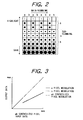
- the exposure amount modulating means 15 modulates density data of two pixels by one (a) [pixel shown by "a" in Fig. 2] of the two pixels and forms one dot and doesn't record the other pixel (b) [pixel shown by "b” in Fig. 2].
- the exposure amount modulating means 15 individually modulates each pixel, thereby forming an image.
- the light scanning apparatus 1 converts the density data based on the image information to an exposure amount of the laser beam through the exposure amount modulating means 15.
- the laser beam which was modulated and oscillated by the light scanning apparatus 1 optically scans the surface of the photosensitive drum 7 which rotates in the direction of the arrow R2 in the diagram through the return mirror 2, thereby forming a potential latent image onto the photosensitive drum.
- the surface of the photosensitive drum 7 has previously been charged by the charging means 3.
- a toner as a developing agent is deposited onto the drum surface by the developing means 4 in accordance with the surface potential of the photosensitive drum 7 on which the latent image was potentially formed, thereby forming a visible image.
- a transfer material is pulled out from the sheet cassette 8 of the transfer material by the paper feed roller 9a and is conveyed by the registration roller 9b at a timing synchronized with the rotation of the photosensitive drum 7.
- the transfer charging means 5 transfers the visible image formed on the surface of the photosensitive drum 7 onto the transfer material at a timing matched with the timing to convey the transfer material.
- the transfer material to which the visible image was transferred is conveyed to fixing means 12 by conveying means 11. After the toner was fixed to the transfer material by the fixing means 12, the transfer material is ejected out onto a paper ejection tray 13 provided so as to be projected to the outside of the printer main body 10. After completion of the transfer step, the toner remaining on the surface of the photosensitive drum 7 is removed by the cleaning means 6. An image is formed while repeating the series of processing steps as mentioned above.
- the image is decomposed to pixels arranged in the main-scanning direction of a raster-shape as shown in Fig. 2.
- a highlight density region as density data in which image densities of two pixels a and b which are adjoining in the main-scanning direction are, for example, equal to or less than 1/3 of the maximum image density (in case of the data in a range in the sub-scanning direction shown at A in Fig. 2)
- the exposure amount modulating means 15 on the light scanning apparatus 1 in the embodiment 1 adds the density data of two pixels, modulates the addition result by one pixel a, forms one dot, and doesn't perform the recording of the other pixel b.
- the exposure amount modulating means 15 individually modulates each pixel and forms an image.
- Fig. 3 shows the relation of the individual or synthesized output data which is modulated for the synthesized input data of the two adjoining pixels a and b.
- a dot which is formed by modulating the density data of the two adjoining pixels by one of the two pixels is dense and large.
- the dot is thin and small and an exposure amount which is generated for each pixel is small, so that the toner is not deposited. Therefore, an inconvenience such that the image is extinguished in the highlight density region or a coarseness of the image which occurs because a size of each dot that is formed by the toner doesn't become stable and varies are reduced.
- a density reproducibility and a density uniformity in the highlight density region are improved.
- the density data of the two adjoining pixels is modulated by one pixel c [pixel shown by "c” in Fig. 4] and two dots are formed and the other pixel d [pixel shown by "d” in Fig. 4] is recorded.
- the exposure amount modulating means 15 which is used in the embodiment 2 sets the pixel c which was modulated in the highlight density region to a fixed value as shown in Fig.
- the density data of two pixels is modulated by one of the two pixels and the other pixel is not recorded, thereby reducing the pixel density in only the highlight density region to the half in the main-scanning direction. Therefore, even if the deterioration in resolution or the increase in moire intensity occur in the highlight density region in which the image densities are equal to or less than 1/3 of the maximum image density, since the density region is the highlight density region, such phenomena are visually inconspicuous. Thus, a sharpness as a whole output image doesn't deteriorate, the generation intensity of the moire is not raised, the image in the highlight density portion can be stably outputted, and an image of a high picture quality can be outputted.
- the density data of two adjoining pixels is modulated by the density data of one of the two pixels and the other pixel is not recorded.
- the light scanning means for forming the latent image onto the photosensitive material is provided with the exposure amount modulating means for modulating the exposure amount in accordance with the pixel density information and expressing a dark/light state of the image for the pixels divided into a predetermined size on the photosensitive material.
- the exposure amount modulating means divides the image density region into the highlight density region, halftone density region, or dark density region, modulates the density data of a predetermined number of continuous pixels in the light scanning direction by the density data of some of the pixels in the highlight density region, and doesn't record the remaining pixels. It is possible to prevent the formation of a dot which is so small that the image formation cannot be stably performed.
- the resolution doesn't deteriorate and an image with a high sharpness can be outputted.
- An image of the highlight density portion can be stably outputted without raising the generation intensity of the moire.
- An image of a high picture quality can be outputted.
- one pixel modulated in the highlight density region is set to the fixed value and as for the other pixel, the data in which the fixed value is subtracted from the density data of two pixels is modulated, so that a pseudo outline is not generated in the output image.
- the dark density region by individually modulating each pixel, the resolution in the dark density region doesn't deteriorate. Thus, the image of a high sharpness can be outputted. The generation intensity of the moire is also suppressed. The image of a high picture quality can be outputted.
- Fig. 6 is a diagram showing a schematic construction of an image forming apparatus of a form of the third embodiment of the invention. Although a construction of the image forming apparatus is substantially the same as that of the apparatus shown in Fig. 1, it will be explained hereinbelow.
- Reference numeral 101 denotes a light scanning unit having a laser diode and a laser diode oscillation control circuit (not shown).
- the light scanning unit 101 oscillates in accordance with image data which is transferred from a control unit 114 and forms an electrostatic latent image onto a drum cylinder 107.
- Reference numeral 102 denotes a return mirror for scanning a laser beam from the light scanning unit 101 onto the drum cylinder 107.
- Reference numeral 103 denotes a charging unit for charging a photosensitive conductor material on the surface of the drum cylinder 107.
- Reference numeral 104 denotes a developing unit for developing the electrostatic latent image formed on the photosensitive conductor material on the surface of the drum cylinder 107.
- Reference numeral 105 denotes a transfer unit for transferring the formed image which was developed by the developing unit 104 onto a transfer material.
- Reference numeral 106 denotes a cleaning unit for removing the remaining toner or the like after completion of the transfer by the transfer unit 105.
- Reference numeral 107 denotes the drum cylinder.
- a photosensitive conductor material is coated onto the surface of the drum cylinder 107.
- the drum cylinder 107 rotates in the direction shown by an arrow in the diagram.
- Reference numeral 108 denotes a cassette to supply transfer material (not shown); 109 a paper feed roller to take out the transfer material (not shown) from the cassette; 110 a conveying roller for conveying the transfer material (not shown); and 111 a conveying belt to convey the transfer material.
- Reference numeral 112 denotes a fixing unit for fixing the image formed by transferring the developing agent onto the transfer material.
- Reference numeral 113 denotes an ejection tray to hold the transfer material ejected to the outside of the apparatus.
- Reference numeral 114 denotes the control unit for performing a density process, which will be explained hereinafter, to the image read data inputted from a scanner unit 115 and transferring the processed data to the light scanning unit 101.
- Reference numeral 115 denotes the scanner unit for optically reading an original image, converting the signal obtained to a digital signal, and transferring to the control unit 114.
- the light scanning unit 101 operates in a manner such that an oscillated light which is generated from a built-in laser diode (not shown) is reflected by the return mirror 102.
- a developing agent for example, toner
- the visible image deposited on the surface of the photosensitive conductor material is transferred by the transfer unit 105 to the transfer material (not shown) which is conveyed by the conveying roller 110 at a predetermined timing.
- the transfer material (not shown) to which the visible image was transferred is conveyed by the conveying belt 111 to the fixing unit 112.
- the visible image transferred onto the transfer material is semipermanently fixed by the fixing unit 112. After that, the transfer material is ejected onto the ejection tray 113 on the outside of the apparatus.
- the developing agent remaining on the drum cylinder 107 is removed by the cleaning unit 106 by rotating the drum cylinder 107.
- the image data which is transferred to the control unit 114 is the image data read out from the scanner, namely, although the apparatus shown in Fig. 1 is a copying apparatus, the embodiment can be also easily applied to a printer which handles image data that is transferred from a host computer.
- Fig. 7 is a block diagram showing a main section of the control unit 114 of the form of the embodiment.
- Reference numeral 121 denotes a CPU for performing controls of a reading of image data into a line memory 122, a process of a density processing unit 123, a transfer of the processed image data to the light scanning unit, and the like.
- Reference numeral 122 denotes a line memory for storing the image data inputted from the scanner unit 115.
- Reference numeral 123 denotes the density processing unit for detecting density data of the image data that is sequentially read out from the line memory 122 and executing processes of the density data of the form of the embodiment, which will be explained hereinlater.
- the density processed data is outputted to the light scanning unit 101.
- the density processing unit 123 in the case where the density data of two adjoining pixels in the raster direction (main-scanning direction) is a and b and the image density is equal to or less than the halftone density, namely, in the case where the image density is smaller than C [C denotes the maximum density of an image to be formed by the image forming apparatus] (C > a + b), the density data of the pixel of density data b is transposed to the pixel of density data a in accordance with arithmetic operations of the following equations (1), thereby newly converting to the pixels having density data of a' and b'.
- the output result in each gradation of the pixel of the density data a and the pixel of the density data b is as shown in Fig. 8.
- the pixels which are adjoining in the main-scanning direction have the same value.
- the density data of the pixel of the density data b is transposed to the pixel of the density data a in accordance with the equations (1) and the resultant data is generated as output image data, so that a difference occurs between the output results of the pixel of the density data a and the pixel of the density data b.
- the output results of the output image data of the pixel of the density data a and the pixel of the density data b are the same.
- the output image data for the input image data of the pixel of the density data a and the pixel of the density data b have characteristics as shown in Fig. 9.
- a transposition ratio of the density data from the pixel of the density data b to the pixel of the density data a gradually increases from the density region in which the density data of each pixel has the half value of the maximum value, namely, from the halftone density region to the highlight density region.
- the density data is minimum, all of the density data of the pixels of the density data b is transposed to the pixel of the density data a.
- the relation between the input and output of the image data in which the pixel of the density data a and the pixel of the density data b are added is linear as shown in Fig. 10.
- the density of the output data is preserved, the pixel of the density data a and the pixel of the density data b lie within a low density region and the pixel densities equivalently decrease, so that the gradation reproducibility in the low density region is improved.
- the resolution is preserved.
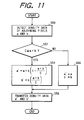
- Fig. 11 is a flowchart showing the operation of the density processing unit of the form of the embodiment.
- step S50 the density data a and b of the adjoining pixels among the pixels arranged in the raster direction of the line memory 122 is detected.
- step S52 the sum (a + b) of the density data of the pixels is calculated on the basis of the density data of the pixels which were detected.
- step S54 the processing routine advances to step S54.
- step S56 follows.
- step S54 When (a + b) is equal to or smaller than C, in step S54, a' and b' are calculated as new density data in accordance with the equations (1) and are set to the density data of the pixels.
- step S58 the density data a' and b' is transferred to the light scanning unit 101 as density data of the image data.
- the image data which was sequentially stored in the line memory 122 is properly converted to a desired density by the density processing unit 123 and is transferred to the light scanning unit 101.
- the transposition ratio of the pixel of the density data b can be also changed as shown by the equations (2).
- a' a + b[1 - ⁇ (a + b ⁇ /C)x]
- b' b ⁇ (a + b)/C ⁇ x
- the transposition ratio of the b density changes in accordance with an xth-order function (x is a positive real number of 1 or more)
- x is a positive real number of 1 or more
- the transposition ratio of the density data rises, the gradation can be smoothly expressed in the highlight region, and the gradation reproducibility is improved.
- the resolution in the highlight region deteriorates.
- a preferred value of x is set to 2 to 3.
- the pixel density of the main-scanning in the highlight density region is close to the half and the gradation reproducibility to the output image data for the input image data can be improved.
- the output image data can be drawn at a high fidelity by the pixel density of the input image data, so that the resolution of the output image data can be improved.
- the case using the laser beam printer has been described.
- the invention can be also applied to an ink jet printer or the like for recording by an emission of an ink.
- the value of x in the equations (2) can be also set from a console panel or a host computer.
- the method shown in the embodiment can be applied to a system constructed by a plurality of equipment or can be also applied to an apparatus comprising one equipment. It will be obviously understood that the invention can be also applied to a case where it is embodied by supplying a program to a system or an apparatus.
- a memory medium in which a program according to the invention has been stored constructs the invention. By reading the program from the memory medium to the system or apparatus, the system or apparatus operates in accordance with a predetermined method.
- the image forming apparatus and method which can improve the gradation reproducibility while preferably preserving the resolution of the recording image data can be provided.
- an image processing method whereby even in an apparatus such that an image forming density of the image forming apparatus can be visually resolved in least distance of distinct vision, an image can be formed so that a linear density of a formed image cannot be visually resolved in least distance of distinct vision.
- a resolution of the main-scanning direction of the image forming apparatus is set to 400 d.p.i.
- the density processing unit 123 in the case where the density data of two adjoining pixels in the raster direction (main-scanning direction) is set to a and b and the image density is equal to or less than the halftone density, namely, when the image density is smaller than C/2 [C denotes the maximum density of an image to be formed by the image forming apparatus] (C/2 > a + b), the density data is transposed in accordance with the following arithmetic operations, thereby newly converting to the pixel having the density data of a' and b'.
- the dot arrangement in the low density region becomes a zigzag lattice arrangement and lines of a resolution which is equal to 283 l.p.i. (lines per inch) at an angle of 45° for the main-scanning direction are formed. Since those lines have a density of 250 d.p.i. or more as will be explained hereinlater, the density level is set to a level such that the dot structure cannot be confirmed by the human eyes in least distance of distinct vision.
- Fig. 12 shows a dot pattern which is obtained by processing the image data of the density gradation which gradually increases from the top to the bottom, namely, from the upper position to the lower position in the sub-scanning direction.
- dots are formed like a lattice of an angle of 45° and have a construction of 45° and 283 l.p.i.
- a limit which can be visually resolved by the human eyes in least distance of distinct vision is about 250 l.p.i. and the dot construction cannot be seen by the eyes.
- the stable dots can be formed as mentioned above and an effect of reduction of the image noises can be obtained.
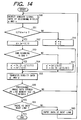
- step S50 the density data a and b of the adjoining pixels [the odd-number designated pixel and the even-number designated pixel] among the pixels arranged in the raster direction in the image data of a plurality of lines stored in the line memory 122 is detected.
- step S51 on the basis of the density data of the pixels which was detected, the sum (a + b) of the density data of the pixels is calculated.
- step S52 the processing routine advances to step S52.
- step S56 follows.
- step S52 When (a + b) is equal to or smaller than C/2, d is calculated in step S52.
- the processing routine advances to step S54. If NO in step S53, namely, the sub-scanning is performed for the even pixel, step S57 follows.
- steps S54 and S57 a' and b' are calculated by the equations shown above and are set to the data of the pixels.
- step S56 When (a + b) is larger than C/2, the density data a and b detected in step S56 is set to the data of the pixels.
- step S55 the density data a' and b' is transferred to the light scanning unit 101 as density data of the images.
- the transposition of the image data for concentration of the dots has been performed by the calculating equations shown in steps S54 and S57 in Fig. 14. According to the calculating equations, however, a degree of concentration of the dots doesn't linearly change but non-linearly changes in accordance with the level of the image signal.
- the dots can be efficiently concentrated and a large effect is obtained.
- Fig. 13 shows image density converting characteristics in the case where the processing steps S51 to S54 and S57 shown in Fig. 14 were executed.
- a solid line shows the characteristics of a when the sub-scanning is performed to the odd pixel, that is, line number of the sub-scanning direction is odd and a broken line shows the characteristics of b.
- the solid line shows b and the broken line shows a.
- the embodiment relates to the case where the invention is applied to a full color image forming apparatus of the electrophotography system having a plurality of drums.
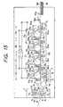
- Fig. 15 is a cross sectional view showing a construction of the full color image forming apparatus of the electrophotography system of the embodiment.
- the apparatus comprises four stations to form images of four colors of magenta, cyan, yellow, and black.
- Photosensitive drums 701a to 701d are uniformly charged by primary charging units 702a to 702d.
- Laser beams emitted from semiconductor lasers (not shown) driven by image signals of the respective colors are scanned and exposed onto the photosensitive drums 701a to 701d by a polygon mirror 17, thereby forming latent images.
- the latent images are developed by developing units 703a to 703d, so that toner images are formed on the photosensitive drums 701a to 701d.
- a recording material 706 put on a recording material tray 60 is picked up by a pickup roller 713a and conveyed into the apparatus by a registration roller 713b.
- the toner images formed on the drums 701a to 701d are transferred onto the recording material 706 which is conveyed by a transfer belt 708.
- the recording material is subsequently conveyed. Registration timings of a plurality of color images on the recording material 706 are matched and images are sequentially multiple transferred by transfer charging units 704a to 704d.
- the transfer sheet 708 is separated by a separation charging unit 14 and by a curvature of a transfer sheet holding roller 710 and is fixed onto the recording material by a fixing roller 71 and a pressurizing roller 72.
- the recording material is subsequently ejected to the outside of the image forming apparatus.
- the fixing roller 71 is formed by coating a silicon rubber and a fluorine rubber onto the surface of a metallic pipe.
- the pressurizing roller 72 is formed by coating a silicon rubber onto the surface of a metal roller.
- Halogen heaters 75 and 76 are controlled by a thermistor 79 attached to the surface of the pressurizing roller 72 and by a temperature control circuit (not shown), thereby controlling the surface temperature to a predetermined value suitable for fixing.
- a silicon oil in an oil pan is pumped and moved to an oil coating roller 77 through a pumping roller 78.
- a predetermined amount of oil is held on the fixing roller 71.
- Each of cleaning devices 73 and 74 uses a beltlike cleaning web member and can always perform the cleaning by a fresh surface by the feeding and take-up of the web.
- the phase of a pattern period of the dot formation is changed by the image forming color.
- Fig. 16 shows an example of formation of a specific dot construction pattern.
- Black circles indicate dots of magenta and black and the dot pattern is formed by the same algorithm as that of the embodiment shown in Fig. 14.
- the black dot fundamentally is not overlaid to the dots of magenta and cyan. Or, a probability such that the black dot is overlaid is small. Therefore, at least the drop of the color information of magenta and cyan can be prevented.
- Fig. 17 is a diagram showing the relation between a toner grain size and an RMS granularity.
- An axis of abscissa of Fig. 17 shows the number of lines of a screen (l.p.i.) and an axis of ordinate indicates the RMS granularity.
- Toners in which the average toner grain sizes are equal to 12, 8, and 5 ⁇ m are used and their RMS granularities are plotted while changing the number of lines of the screen.
- the average toner grain size is smaller than 10 ⁇ m in the case where the number of lines of the screen is equal to 200 l.p.i.
- Fig. 18 shows visual sense MTF characteristics in least distance of distinct vision (about 35 cm).
- An axis of abscissa denotes the resolution and an axis of ordinate indicates the MTF.
- the density level is set to a level at which the dot structure is not recognized by the observer.
- the types shown by A, B, and C in Fig. 19 relate to the commercially available apparatuses. Laser beam sizes and toner grain sizes corresponding to the types are set to the values as shown in the diagram. According to the commercially available types, the image processing shown in the present specification and drawings is not adopted.
- the laser beam size is equal to 45 ⁇ m ⁇ 65 ⁇ m and the toner grain size lies within a range from 5 to 6 ⁇ m. Further, the image processing method shown in the specification is adopted.
- the toner of the grain size of 5 ⁇ m is adopted from the above characteristics, the image signal of 400 l.p.i. is used, the image processing to concentrate the dots is performed, an image is formed at an angle of 45° and a resolution of 283 l.p.i.
- the image noises are reduced as much as possible.
- the image in which the dot structure cannot be recognized under the ordinary observing conditions could be formed.
- the scanning means for scanning a digital image signal necessary to form a color image and forming an image
- comparing means for comparing the scanned digital image signal with a predetermined image signal value
- modulating means for modulating the signal in accordance with the image signal for a group of pixels divided to a predetermined size and expressing an image dark/light state
- the signal value is modulated by the modulating means in the pixels divided into the predetermined size
- the size of the pixel group divided into the predetermined size is set to a size which cannot be visually resolved in least distance of distinct vision
Landscapes
- Engineering & Computer Science (AREA)
- Multimedia (AREA)
- Signal Processing (AREA)
- Color, Gradation (AREA)
- Facsimile Image Signal Circuits (AREA)
- Laser Beam Printer (AREA)
- Fax Reproducing Arrangements (AREA)
Applications Claiming Priority (9)
| Application Number | Priority Date | Filing Date | Title |
|---|---|---|---|
| JP316704/94 | 1994-12-20 | ||
| JP31670494 | 1994-12-20 | ||
| JP31670494 | 1994-12-20 | ||
| JP17598995 | 1995-07-12 | ||
| JP175989/95 | 1995-07-12 | ||
| JP17598995 | 1995-07-12 | ||
| JP32733495 | 1995-12-15 | ||
| JP7327334A JPH0983799A (ja) | 1994-12-20 | 1995-12-15 | 画像処理方法及び装置それを用いた画像形成方法及び装置 |
| JP327334/95 | 1995-12-15 |
Publications (3)
| Publication Number | Publication Date |
|---|---|
| EP0719033A2 true EP0719033A2 (fr) | 1996-06-26 |
| EP0719033A3 EP0719033A3 (fr) | 1997-05-02 |
| EP0719033B1 EP0719033B1 (fr) | 2001-11-14 |
Family
ID=27324189
Family Applications (1)
| Application Number | Title | Priority Date | Filing Date |
|---|---|---|---|
| EP95309245A Expired - Lifetime EP0719033B1 (fr) | 1994-12-20 | 1995-12-19 | Procédé et appareil de traitement d'images |
Country Status (4)
| Country | Link |
|---|---|
| US (3) | US6016206A (fr) |
| EP (1) | EP0719033B1 (fr) |
| JP (1) | JPH0983799A (fr) |
| DE (1) | DE69523882T2 (fr) |
Cited By (3)
| Publication number | Priority date | Publication date | Assignee | Title |
|---|---|---|---|---|
| WO2002082801A1 (fr) * | 2001-03-09 | 2002-10-17 | Hewlett-Packard Company | Procede et systeme de diffusion d'erreur par points partiels |
| EP1435728A3 (fr) * | 2003-01-06 | 2005-11-16 | Agfa Corporation | Procédé et système pour l'obtention de demi-teintes utilisant un tramage hybride AM/FM pour des zones de tonalités claires et sombres |
| EP1257113A3 (fr) * | 2001-05-11 | 2006-04-12 | Seiko Epson Corporation | Impression par plusieurs éléments d'image comme unité pour la reproduction de gradations |
Families Citing this family (15)
| Publication number | Priority date | Publication date | Assignee | Title |
|---|---|---|---|---|
| US6226019B1 (en) * | 1997-12-26 | 2001-05-01 | Canon Kabushiki Kaisha | Imaging forming apparatus for forming an image by digital processing |
| JPH11205603A (ja) * | 1998-01-19 | 1999-07-30 | Toshiba Corp | 画像処理装置と画像形成装置 |
| DE69900123T2 (de) * | 1998-03-12 | 2001-10-18 | Brother Kogyo K.K., Nagoya | Druckgerät, Druckersystem und Speichermedium |
| JPH11295939A (ja) * | 1998-04-07 | 1999-10-29 | Hitachi Ltd | 電子写真記録装置 |
| US6791713B1 (en) * | 1998-10-13 | 2004-09-14 | Ricoh Company, Ltd. | Image forming apparatus |
| DE60035549T2 (de) * | 1999-06-07 | 2008-04-17 | Canon K.K. | Bildaufzeichnungsgerät und Verfahren |
| JP2002328551A (ja) * | 2001-04-27 | 2002-11-15 | Ricoh Co Ltd | 画像形成方法および画像形成装置 |
| US6781719B2 (en) * | 2002-06-27 | 2004-08-24 | Hewlett-Packard Development Company, L.P. | Halftone imaging with reduced dot isolation |
| JP2004306555A (ja) * | 2003-04-10 | 2004-11-04 | Seiko Epson Corp | 印刷処理装置及び印刷処理方法 |
| US7602411B2 (en) * | 2003-06-12 | 2009-10-13 | Oki Data Corporation | Image forming apparatus |
| US7373011B2 (en) * | 2004-10-07 | 2008-05-13 | Polaroid Corporation | Density-dependent sharpening |
| US7755654B2 (en) * | 2006-07-25 | 2010-07-13 | Hewlett-Packard Development Company, L.P. | Pixel |
| US8200022B2 (en) * | 2008-03-24 | 2012-06-12 | Verint Systems Ltd. | Method and system for edge detection |
| JP4875723B2 (ja) * | 2009-04-24 | 2012-02-15 | シャープ株式会社 | 画像形成装置 |
| JP6322922B2 (ja) * | 2013-08-08 | 2018-05-16 | 株式会社リコー | 画像形成方法、画像形成装置 |
Family Cites Families (13)
| Publication number | Priority date | Publication date | Assignee | Title |
|---|---|---|---|---|
| JPS6062779A (ja) * | 1983-08-31 | 1985-04-10 | Nec Corp | インクジェット記録方法 |
| US4890121A (en) * | 1985-01-31 | 1989-12-26 | Kabushiki Kaisha Toshiba | Halftone image printing device |
| US5148287A (en) * | 1988-10-20 | 1992-09-15 | Canon Kabushiki Kaisha | Image processing apparatus with good highlight reproduction |
| US5148387A (en) * | 1989-02-22 | 1992-09-15 | Hitachi, Ltd. | Logic circuit and data processing apparatus using the same |
| JPH02303863A (ja) * | 1989-05-19 | 1990-12-17 | Canon Inc | 画像形成装置 |
| US5124802A (en) * | 1989-09-26 | 1992-06-23 | Canon Kabushiki Kaisha | Electrostatic lasar printer with a short side length of a modulation area formed by pulse width modulation set relative to a detected toner particle size |
| JP2824999B2 (ja) * | 1990-02-01 | 1998-11-18 | キヤノン株式会社 | 画像処理装置 |
| JP2715337B2 (ja) | 1990-10-26 | 1998-02-18 | キヤノン株式会社 | 画像形成方法 |
| JPH04316276A (ja) * | 1991-04-16 | 1992-11-06 | Ricoh Co Ltd | 画像形成装置 |
| JP3244811B2 (ja) * | 1992-02-04 | 2002-01-07 | キヤノン株式会社 | 記録装置及び画像処理方法 |
| US5418618A (en) * | 1992-03-09 | 1995-05-23 | Mita Industrial Co., Ltd. | Tone processing method for forming a halftone image |
| EP0564868A3 (en) * | 1992-04-06 | 1993-11-10 | Konishiroku Photo Ind | Image forming apparatus |
| JPH0683951A (ja) * | 1992-09-02 | 1994-03-25 | Ricoh Co Ltd | 画像形成装置及びその2値画像データのスムージング拡大処理方法 |
-
1995
- 1995-12-15 JP JP7327334A patent/JPH0983799A/ja not_active Withdrawn
- 1995-12-19 DE DE69523882T patent/DE69523882T2/de not_active Expired - Fee Related
- 1995-12-19 US US08/575,141 patent/US6016206A/en not_active Expired - Fee Related
- 1995-12-19 EP EP95309245A patent/EP0719033B1/fr not_active Expired - Lifetime
-
1999
- 1999-10-29 US US09/429,492 patent/US6304341B1/en not_active Expired - Fee Related
- 1999-10-29 US US09/430,026 patent/US6190058B1/en not_active Expired - Fee Related
Cited By (4)
| Publication number | Priority date | Publication date | Assignee | Title |
|---|---|---|---|---|
| WO2002082801A1 (fr) * | 2001-03-09 | 2002-10-17 | Hewlett-Packard Company | Procede et systeme de diffusion d'erreur par points partiels |
| US6778299B2 (en) | 2001-03-09 | 2004-08-17 | Hewlett-Packard Development Company, L.P. | Error diffusion with partial dots method and system |
| EP1257113A3 (fr) * | 2001-05-11 | 2006-04-12 | Seiko Epson Corporation | Impression par plusieurs éléments d'image comme unité pour la reproduction de gradations |
| EP1435728A3 (fr) * | 2003-01-06 | 2005-11-16 | Agfa Corporation | Procédé et système pour l'obtention de demi-teintes utilisant un tramage hybride AM/FM pour des zones de tonalités claires et sombres |
Also Published As
| Publication number | Publication date |
|---|---|
| US6304341B1 (en) | 2001-10-16 |
| JPH0983799A (ja) | 1997-03-28 |
| DE69523882T2 (de) | 2002-06-13 |
| DE69523882D1 (de) | 2001-12-20 |
| EP0719033B1 (fr) | 2001-11-14 |
| EP0719033A3 (fr) | 1997-05-02 |
| US6016206A (en) | 2000-01-18 |
| US6190058B1 (en) | 2001-02-20 |
Similar Documents
| Publication | Publication Date | Title |
|---|---|---|
| EP0719033B1 (fr) | Procédé et appareil de traitement d'images | |
| US5467196A (en) | Image forming apparatus which forms halftone images mixed with characters and fine lines | |
| JP5512522B2 (ja) | Mtfの適応可能な補正のための方法、装置、およびコンピュータプログラム | |
| EP0264754A2 (fr) | Procédé d'enregistrement d'images en semi-demi-teintes | |
| US7224488B2 (en) | Method of correcting threshold array, dot pattern data structure, method of correcting pixel layout of image, and method of determining threshold array for generating image | |
| US5708514A (en) | Error diffusion method in a multi-level image recording apparatus utilizing adjacent-pixel characteristics | |
| US6704123B1 (en) | Method for applying tonal correction to a binary halftone image | |
| US8610962B2 (en) | Screen design for process variation artifact reduction | |
| EP1017018B1 (fr) | Procédé et appareil pour la rotation d'image à haute facilité d'adressage | |
| US6954556B2 (en) | Smoothing method, smoothing circuit and image output apparatus | |
| US6552824B2 (en) | Method of processing pixels with binary or multibit error diffusion | |
| EP0465074B1 (fr) | Appareil pour former des images | |
| JP3373556B2 (ja) | 画像形成装置 | |
| US6765692B1 (en) | Image processing method and apparatus and image forming method and apparatus using the same | |
| JP3862769B2 (ja) | 画像記録装置 | |
| JP3147458B2 (ja) | デジタル画像形成法 | |
| JP2003287931A (ja) | 画像形成装置およびその調整方法 | |
| JP3244081B2 (ja) | 電子写真装置及び電子写真の画像処理方法 | |
| US6226108B1 (en) | Image processing apparatus and method for reproducing high quality image in low-density portion | |
| JP2000094756A (ja) | 電子写真の画像処理装置及びその方法 | |
| JP3789126B2 (ja) | 画像記録装置 | |
| JPH10166658A (ja) | 画像形成装置 | |
| JPH1117947A (ja) | 画像形成方法及び画像形成装置 | |
| US5446561A (en) | Method and apparatus for digital scale halftoning with variable screen structure for electrophotographic printing devices | |
| JPH0869139A (ja) | 画像形成方法および装置 |
Legal Events
| Date | Code | Title | Description |
|---|---|---|---|
| PUAI | Public reference made under article 153(3) epc to a published international application that has entered the european phase |
Free format text: ORIGINAL CODE: 0009012 |
|
| AK | Designated contracting states |
Kind code of ref document: A2 Designated state(s): DE FR GB IT |
|
| PUAL | Search report despatched |
Free format text: ORIGINAL CODE: 0009013 |
|
| AK | Designated contracting states |
Kind code of ref document: A3 Designated state(s): DE FR GB IT |
|
| 17P | Request for examination filed |
Effective date: 19970917 |
|
| 17Q | First examination report despatched |
Effective date: 19991026 |
|
| RTI1 | Title (correction) |
Free format text: IMAGE PROCESSING METHOD AND APPARATUS |
|
| GRAG | Despatch of communication of intention to grant |
Free format text: ORIGINAL CODE: EPIDOS AGRA |
|
| RTI1 | Title (correction) |
Free format text: IMAGE PROCESSING METHOD AND APPARATUS |
|
| GRAG | Despatch of communication of intention to grant |
Free format text: ORIGINAL CODE: EPIDOS AGRA |
|
| GRAH | Despatch of communication of intention to grant a patent |
Free format text: ORIGINAL CODE: EPIDOS IGRA |
|
| GRAH | Despatch of communication of intention to grant a patent |
Free format text: ORIGINAL CODE: EPIDOS IGRA |
|
| GRAA | (expected) grant |
Free format text: ORIGINAL CODE: 0009210 |
|
| AK | Designated contracting states |
Kind code of ref document: B1 Designated state(s): DE FR GB IT |
|
| PG25 | Lapsed in a contracting state [announced via postgrant information from national office to epo] |
Ref country code: IT Free format text: LAPSE BECAUSE OF FAILURE TO SUBMIT A TRANSLATION OF THE DESCRIPTION OR TO PAY THE FEE WITHIN THE PRE;WARNING: LAPSES OF ITALIAN PATENTS WITH EFFECTIVE DATE BEFORE 2007 MAY HAVE OCCURRED AT ANY TIME BEFORE 2007. THE CORRECT EFFECTIVE DATE MAY BE DIFFERENT FROM THE ONE RECORDED.SCRIBED TIME-LIMIT Effective date: 20011114 Ref country code: FR Free format text: LAPSE BECAUSE OF FAILURE TO SUBMIT A TRANSLATION OF THE DESCRIPTION OR TO PAY THE FEE WITHIN THE PRESCRIBED TIME-LIMIT Effective date: 20011114 |
|
| REF | Corresponds to: |
Ref document number: 69523882 Country of ref document: DE Date of ref document: 20011220 |
|
| REG | Reference to a national code |
Ref country code: GB Ref legal event code: IF02 |
|
| PLBE | No opposition filed within time limit |
Free format text: ORIGINAL CODE: 0009261 |
|
| STAA | Information on the status of an ep patent application or granted ep patent |
Free format text: STATUS: NO OPPOSITION FILED WITHIN TIME LIMIT |
|
| EN | Fr: translation not filed | ||
| 26N | No opposition filed | ||
| PGFP | Annual fee paid to national office [announced via postgrant information from national office to epo] |
Ref country code: GB Payment date: 20061218 Year of fee payment: 12 |
|
| PGFP | Annual fee paid to national office [announced via postgrant information from national office to epo] |
Ref country code: DE Payment date: 20070219 Year of fee payment: 12 |
|
| GBPC | Gb: european patent ceased through non-payment of renewal fee |
Effective date: 20071219 |
|
| PG25 | Lapsed in a contracting state [announced via postgrant information from national office to epo] |
Ref country code: DE Free format text: LAPSE BECAUSE OF NON-PAYMENT OF DUE FEES Effective date: 20080701 |
|
| PG25 | Lapsed in a contracting state [announced via postgrant information from national office to epo] |
Ref country code: GB Free format text: LAPSE BECAUSE OF NON-PAYMENT OF DUE FEES Effective date: 20071219 |