EP0719078A2 - Zusammenbau von Leiterplatten mit einer verbesserten Isolierung der Bezugsebene - Google Patents
Zusammenbau von Leiterplatten mit einer verbesserten Isolierung der Bezugsebene Download PDFInfo
- Publication number
- EP0719078A2 EP0719078A2 EP95109836A EP95109836A EP0719078A2 EP 0719078 A2 EP0719078 A2 EP 0719078A2 EP 95109836 A EP95109836 A EP 95109836A EP 95109836 A EP95109836 A EP 95109836A EP 0719078 A2 EP0719078 A2 EP 0719078A2
- Authority
- EP
- European Patent Office
- Prior art keywords
- pca
- reference plane
- single file
- layer
- apertures
- Prior art date
- Legal status (The legal status is an assumption and is not a legal conclusion. Google has not performed a legal analysis and makes no representation as to the accuracy of the status listed.)
- Granted
Links
- 238000002955 isolation Methods 0.000 title claims abstract description 20
- 238000004891 communication Methods 0.000 claims abstract description 14
- 239000004020 conductor Substances 0.000 claims description 21
- 239000007787 solid Substances 0.000 claims description 8
- 238000013461 design Methods 0.000 description 7
- 230000000694 effects Effects 0.000 description 4
- 230000001965 increasing effect Effects 0.000 description 4
- 238000005259 measurement Methods 0.000 description 4
- RYGMFSIKBFXOCR-UHFFFAOYSA-N Copper Chemical compound [Cu] RYGMFSIKBFXOCR-UHFFFAOYSA-N 0.000 description 2
- 230000008901 benefit Effects 0.000 description 2
- 229910052802 copper Inorganic materials 0.000 description 2
- 239000010949 copper Substances 0.000 description 2
- 238000000034 method Methods 0.000 description 2
- DSPDJPFEBQTXDO-UHFFFAOYSA-N 1-[2-(3-pyrrolidin-1-ylprop-1-ynyl)piperidin-1-yl]ethanone Chemical compound CC(=O)N1CCCCC1C#CCN1CCCC1 DSPDJPFEBQTXDO-UHFFFAOYSA-N 0.000 description 1
- 230000000712 assembly Effects 0.000 description 1
- 238000000429 assembly Methods 0.000 description 1
- 230000005540 biological transmission Effects 0.000 description 1
- 230000008859 change Effects 0.000 description 1
- 238000006243 chemical reaction Methods 0.000 description 1
- 238000010586 diagram Methods 0.000 description 1
- 230000006872 improvement Effects 0.000 description 1
- 230000001939 inductive effect Effects 0.000 description 1
- 238000004519 manufacturing process Methods 0.000 description 1
- 230000004048 modification Effects 0.000 description 1
- 238000012986 modification Methods 0.000 description 1
- 230000000149 penetrating effect Effects 0.000 description 1
- 230000005855 radiation Effects 0.000 description 1
- 230000009467 reduction Effects 0.000 description 1
- 230000001105 regulatory effect Effects 0.000 description 1
- 238000000926 separation method Methods 0.000 description 1
- 239000011800 void material Substances 0.000 description 1
Images


Classifications
-
- H—ELECTRICITY
- H05—ELECTRIC TECHNIQUES NOT OTHERWISE PROVIDED FOR
- H05K—PRINTED CIRCUITS; CASINGS OR CONSTRUCTIONAL DETAILS OF ELECTRIC APPARATUS; MANUFACTURE OF ASSEMBLAGES OF ELECTRICAL COMPONENTS
- H05K9/00—Screening of apparatus or components against electric or magnetic fields
- H05K9/0007—Casings
- H05K9/002—Casings with localised screening
- H05K9/0039—Galvanic coupling of ground layer on printed circuit board [PCB] to conductive casing
-
- H—ELECTRICITY
- H05—ELECTRIC TECHNIQUES NOT OTHERWISE PROVIDED FOR
- H05K—PRINTED CIRCUITS; CASINGS OR CONSTRUCTIONAL DETAILS OF ELECTRIC APPARATUS; MANUFACTURE OF ASSEMBLAGES OF ELECTRICAL COMPONENTS
- H05K1/00—Printed circuits
- H05K1/02—Details
- H05K1/0213—Electrical arrangements not otherwise provided for
- H05K1/0216—Reduction of cross-talk, noise or electromagnetic interference
-
- H—ELECTRICITY
- H05—ELECTRIC TECHNIQUES NOT OTHERWISE PROVIDED FOR
- H05K—PRINTED CIRCUITS; CASINGS OR CONSTRUCTIONAL DETAILS OF ELECTRIC APPARATUS; MANUFACTURE OF ASSEMBLAGES OF ELECTRICAL COMPONENTS
- H05K1/00—Printed circuits
- H05K1/02—Details
- H05K1/0213—Electrical arrangements not otherwise provided for
- H05K1/0254—High voltage adaptations; Electrical insulation details; Overvoltage or electrostatic discharge protection ; Arrangements for regulating voltages or for using plural voltages
- H05K1/0262—Arrangements for regulating voltages or for using plural voltages
-
- H—ELECTRICITY
- H05—ELECTRIC TECHNIQUES NOT OTHERWISE PROVIDED FOR
- H05K—PRINTED CIRCUITS; CASINGS OR CONSTRUCTIONAL DETAILS OF ELECTRIC APPARATUS; MANUFACTURE OF ASSEMBLAGES OF ELECTRICAL COMPONENTS
- H05K2201/00—Indexing scheme relating to printed circuits covered by H05K1/00
- H05K2201/09—Shape and layout
- H05K2201/09209—Shape and layout details of conductors
- H05K2201/0929—Conductive planes
- H05K2201/093—Layout of power planes, ground planes or power supply conductors, e.g. having special clearance holes therein
-
- H—ELECTRICITY
- H05—ELECTRIC TECHNIQUES NOT OTHERWISE PROVIDED FOR
- H05K—PRINTED CIRCUITS; CASINGS OR CONSTRUCTIONAL DETAILS OF ELECTRIC APPARATUS; MANUFACTURE OF ASSEMBLAGES OF ELECTRICAL COMPONENTS
- H05K2201/00—Indexing scheme relating to printed circuits covered by H05K1/00
- H05K2201/09—Shape and layout
- H05K2201/09209—Shape and layout details of conductors
- H05K2201/09654—Shape and layout details of conductors covering at least two types of conductors provided for in H05K2201/09218 - H05K2201/095
- H05K2201/09663—Divided layout, i.e. conductors divided in two or more parts
-
- H—ELECTRICITY
- H05—ELECTRIC TECHNIQUES NOT OTHERWISE PROVIDED FOR
- H05K—PRINTED CIRCUITS; CASINGS OR CONSTRUCTIONAL DETAILS OF ELECTRIC APPARATUS; MANUFACTURE OF ASSEMBLAGES OF ELECTRICAL COMPONENTS
- H05K2201/00—Indexing scheme relating to printed circuits covered by H05K1/00
- H05K2201/09—Shape and layout
- H05K2201/09209—Shape and layout details of conductors
- H05K2201/09654—Shape and layout details of conductors covering at least two types of conductors provided for in H05K2201/09218 - H05K2201/095
- H05K2201/0969—Apertured conductors
Definitions
- This invention relates to a printed circuit assembly (PCA) and, more specifically, to a reference plane layer in a PCA having improved Input/Output (I/O) isolation for reducing common mode cable emissions.
- PCA printed circuit assembly
- I/O Input/Output
- common mode potential In computer systems and related printed circuit assemblies (PCAs), digital integrated circuits (ICs) radiate switching noise which can cause emission problems beyond the FCC limits. Similarly, common mode potential (CMP) in a PCA can cause emission problems beyond the limits.
- common mode potential In a PCA, common mode potential is caused by power plane voltage in relation to a ground plane, and their respective current flow. Either the power plane or the ground plane may be considered a reference plane and, in this context, is a solid sheet of conducting material.
- common mode potential or common mode interference can be described as:
- a PCA uses Input/Output (I/O) communications circuitry in conjunction with cabling connections for interconnecting separate circuitry, components, or devices.
- I/O Input/Output
- a common standard for I/O communications is small computer systems interface (SCSI).
- SCSI small computer systems interface
- the reference plane is typically a solid sheet of conducting material in the PCA and does not lend itself to allowing for isolation of the circuitry as stated.
- a non conductive void can be formed in a reference plane by literally removing portions of the plane to isolate the applicable circuitry connections, such voids, in and of themselves, create a slot antenna effect and tend to increase undesirable emissions, i.e., in the form of differential loop emissions, rather than decrease such emissions.
- objects of the present invention are to improve reference plane isolation in a PCA to reduce unacceptable common mode cable emissions without significantly increasing differential mode emissions.
- a printed circuit assembly includes a reference plane layer having a plurality of apertures patterned therein to improve reference plane isolation for reducing electromagnetic emissions and, more specifically, common mode cable emissions.
- a component layer of the PCA includes general PCA functional circuitry (i.e., non Input/Output (I/O) circuitry), such as digital integrated circuitry, and I/O communication circuitry thereon.
- I/O Input/Output
- the apertures are aligned in a double row of substantially single file patterns on the reference plane.
- the single file patterns are positioned substantially parallel to and adjacent each other. Also, each aperture in each single file pattern is staggered with respect to a corresponding aperture in the adjacent single file pattern.
- the patterned apertures are placed relative to the component layer in a manner such that they are substantially perpendicular to signal traces and substantially separate the non I/O circuitry from the I/O communication circuitry for reducing electromagnetic emissions and, more specifically, I/O communication emissions.
- the apertures are aligned in an individual, substantially single file pattern on the reference plane.
- Figure 1 is an exploded perspective view of a PCA having multiple layers and including a reference plane layer of the present invention.
- Figure 2 is a partial plan view of a substantially single file aperture pattern in a PCA reference plane layer of the present invention.
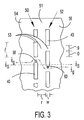
- Figure 3 is a partial plan view of the preferred embodiment having a double row of substantially single file aperture patterns in a PCA reference plane layer.
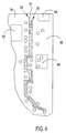
- Figure 4 is a partial plan view of a reference plane having the preferred embodiment double row of slots that substantially separate and isolate the I/O reference plane from the circuit reference plane.
- Figure 1 is an exploded perspective view of PCA 10 having multiple layers (planes) and including a reference plane layer 22 of the present invention. In final assembly, all layers are in contact and electrical trace connections are made. Although six layers are shown in this drawing, it is understood by those of ordinary skill in the art that these six layers are merely representative of this particular PCA. PCA's in general may include any number and variation of layers for embodying the present invention isolated reference plane.
- Top layer 12 is a signal trace and component layer, including digital integrated circuits 14, I/O communication circuitry 15, multiple I/O cable connectors 16, power connectors 18, and multiple signal traces (conductors) 20.
- I/O communication circuitry 15 and cable connectors 16 comply with the small computer systems interface (SCSI) standard.
- SCSI small computer systems interface
- signal traces are included on top layer 12, it is understood that this is only a depicted embodiment and that signal traces in general may not necessarily be on the same layer as the components but may be routed through vias to other layers of the PCA, depending on design criteria or preference.
- digital ICs 14 are merely representative of the general PCA functional circuitry (i.e., non Input/Output (I/O) circuitry), and that other circuitry could likewise be used, such as analog or discrete circuitry.
- the second layer 22 is a ground plane, and in this embodiment, the reference plane.
- the ground plane is, typically, a thin, solid conducting copper sheet.
- a plurality of apertures 23 are patterned in reference plane 22 to improve I/O reference plane isolation for reducing electromagnetic and common mode cable emissions when a cable is connected to cable connectors 16 of top layer 12.
- the apertures are slot shaped, and are aligned in a double row of substantially single file patterns on the reference plane.
- Each single file pattern is positioned substantially parallel to and adjacent the other.
- each aperture in each single file pattern is staggered (offset) with respect to a corresponding aperture in the adjacent single file pattern.
- the single file patterns of apertures 23 are placed on reference plane 22 such that, relative to top signal trace layer 12 in the PCA, they are substantially perpendicular to signal traces 20 (or at least more perpendicular than not in the preferred embodiment). Furthermore, with respect to component layer 12, the apertures substantially separate digital integrated circuitry (non I/O circuitry) 14 from I/O communication circuitry 15 for reducing I/O communication emissions that occur when a cable is connected (not shown) to cable connectors 16.
- the double row of single file apertures 23 are on ground plane 22, and such is considered the reference plane.
- the apertures may similarly be placed on power plane 28.
- ground plane 22 or power plane 28 may be the reference plane, depending on design criteria.
- apertures 23 are defined and placed such that a division of the substantially solid, conducting reference plane occurs creating an isolation effect between integrated circuitry 14 and I/O circuitry 15.
- Apertures 23 are also defined and placed such that differential loop emissions are minimized (the differential loop emissions being caused by return current flow around the apertures).
- the definition and placement of the apertures (1) increases the impedance between the aperture divided portions of the reference plane, and (2) increases the mutual inductance between signal traces 20 of top layer 12 and reference (ground) plane 22. By increasing the impedance, reference plane isolation is improved, and by increasing the mutual inductance the differential current loops in the ground plane (or power plane) are reduced.
- reference plane 22 also includes multiple holes 21 for connections between top layer 12 and third signal trace layer 24. Similar to third layer 24, fourth layer 26 is also a signal trace layer.
- reference plane 22 is a substantially solid conducting sheet having apertures 23 defined therein for isolation purposes
- an alternate method for constructing a reference plane on a PCA is to use a signal layer instead of an internal plane layer and form the reference conductor out of a grid of traces each connected together and all connected to the reference potential.
- the grid can be a uniform pattern of traces or a connection of random-shaped traces. From the standpoint of this invention, it does not matter. Regardless of the pattern of the reference grid, the implementation of this invention is to remove conductors in a single or double row of apertures as stated above. If the reference plane is solid, the shape of the apertures is obvious.
- the detailed shape of the slots may not be as evident since the "slots" may be represented by missing traces in the shape of the slots, but the results are the same.
- the idea is to separate the I/O circuitry currents from the rest of the PCA circuitry currents in such a way as to minimize the I/O reference plane/grid common mode potential.
- the fifth layer 28 is a power plane, have multiple segmented and electrically isolated sections 30, each having different voltages. Except for these isolations, it is substantially a continuous copper sheet having multiple holes and connections similar to ground plane 22.
- the bottom (sixth) layer 32 like top layer 12, contains integrated circuits (not shown) and multiple signal traces 36.
- FIG. 2 a partial plan view is shown which illustrates an individual, substantially single file pattern of apertures (slots) 40 in ground (reference) plane 42.
- the use of the isolated I/O reference plane is to reduce common mode cable emissions that usually emit in the frequency range between 30 and 500 MHz.
- I/O reference plane 44 on one side of ground plane 42 as divided by slots 40, and circuit reference plane 46 on the other side, it is difficult to prevent signal conductors (i.e., traces on their respective PCA layers) from crossing the slots because of routing, design, and fabrication constraints.
- signal conductors i.e., traces on their respective PCA layers
- the return current i g flowing in reference plane 42
- differential loop emissions are caused at frequencies above 300 MHz, depending on the dimensions of the boundary.
- the differential loop emission is a result of the forced different paths between signal trace i s and return signal i g .
- the return ground current in the reference plane would be forced to loop further around the bottom of the slot creating a larger differential loop, and thus larger emissions. Accordingly, when using multiple shorter slots 40, the largest differential loop due to current i g occurs in the case where signal trace current i s is centered over slot 40 as shown in the diagram. It should be noted here that i g in its return path "images" or tries to image signal trace current i s and tends to maximize the mutual inductance and, therefore, minimize the total inductance of the signal ground loop.
- This invention maintains I/O reference plane isolation while minimizing the effects of differential mode emissions by creating the plane isolation out of a series of slots 40, each with a maximum linear dimension small enough to prevent differential loop emissions in the frequency range of interest.
- the maximum frequency range of interest is 2 GHz, the FCC top frequency for emission control.
- the maximum linear slot dimension "m" is the parameter that controls the effective differential loop emission frequency. For example, a square with sides equal to 1 unit emits the same as a circle of diameter 1.41 units. This is due to the maximum linear dimension of the square being the diagonal between two corners, or ⁇ 2.
- the signals i g flowing around slot 40 in ground plane conductor 42 form an emission source analogous to a dipole antenna.
- the emissions from this antenna increase as the slot dimensions increase toward the wavelength of the signal. In other words, it is important to maintain slot lengths that are short in comparison to the wavelength of the emission signal of interest in the dielectric of the printed circuit board.
- the signal of interest here is the maximum frequency specified by the FCC for this class, i.e., 2 GHz.
- the width "w" of slot 40, and end-to-end gap "g" are set at the minimum design criteria measurement relating to a minimum manufacturable distance for this type of device. In this case, 0.005 inches for both measurements is about the minimum manufacturable distance.
- the impedance of the conductors 41 between the ends of the slots affects the isolation between the two conductive planes 44 and 46.
- the dimension of the inter-plane connections 41 is defined by "w” and "g". Namely, the conductor is effectively "w" long and "g" wide.
- each slot 40 in single file pattern 50 is offset staggered distance "o" with reference to each corresponding slot 40 in pattern 52.
- each slot 40 in single file pattern 50 is spaced distance "r” from each corresponding slot 40 in pattern 52.
- measurement "r” is also preferably set at the minimum design criteria measurement relating to a minimum manufacturable distance for this type of device, i.e., about 0.005 inches.
- distance "o” is preferably 1 ⁇ 2 the length "l”.
- magnetic field 60 created due to ground return current i g flowing around the first row of slots 52, will destructively interfere with the magnetic field 58, created due to return current i g continuing to flow around the second row of slots 50.
- the shielding loss is small, especially when the length "l" of the slot and the row-to-row spacing "r" are kept at a minimum, and as mentioned, the overlap (stagger) dimension "o" is about 1 ⁇ 2 the length "l".
- the double row of slots 50 and 52 is shown substantially separating the circuit reference plane 54 from the I/O reference plane 56.
- the zig-zag nature of the rows is due to the placement of the IC components on a component layer of the PCA (see top layer 12 of Figure 1).
- this placement of the slots is to effectively and substantially separate the digital integrated circuitry components 62 (which actually reside on the component layer) from the I/O circuitry 64 (also on the component layer).
- a power plane layer (30 of Figure 1) is being isolated as a reference plane
- a functionally similar type of separation would be used depending on the location of any adjacent layer components (32 of Figure 1).
Landscapes
- Engineering & Computer Science (AREA)
- Microelectronics & Electronic Packaging (AREA)
- Physics & Mathematics (AREA)
- Electromagnetism (AREA)
- Structure Of Printed Boards (AREA)
- Shielding Devices Or Components To Electric Or Magnetic Fields (AREA)
- Production Of Multi-Layered Print Wiring Board (AREA)
Applications Claiming Priority (2)
| Application Number | Priority Date | Filing Date | Title |
|---|---|---|---|
| US370770 | 1994-12-22 | ||
| US08/370,770 US5523921A (en) | 1994-12-22 | 1994-12-22 | Printed circuit assembly having improved reference plane isolation |
Publications (3)
| Publication Number | Publication Date |
|---|---|
| EP0719078A2 true EP0719078A2 (de) | 1996-06-26 |
| EP0719078A3 EP0719078A3 (de) | 1997-05-14 |
| EP0719078B1 EP0719078B1 (de) | 1999-02-24 |
Family
ID=23461098
Family Applications (1)
| Application Number | Title | Priority Date | Filing Date |
|---|---|---|---|
| EP95109836A Expired - Lifetime EP0719078B1 (de) | 1994-12-22 | 1995-06-23 | Zusammenbau von Leiterplatten mit einer verbesserten Isolierung der Bezugsebene |
Country Status (4)
| Country | Link |
|---|---|
| US (1) | US5523921A (de) |
| EP (1) | EP0719078B1 (de) |
| JP (1) | JPH08242079A (de) |
| DE (1) | DE69507938T2 (de) |
Families Citing this family (15)
| Publication number | Priority date | Publication date | Assignee | Title |
|---|---|---|---|---|
| DE9300868U1 (de) * | 1993-01-22 | 1994-05-26 | Siemens AG, 80333 München | Einstückiges Isolierteil, insbesondere Spritzgießteil |
| US5841074A (en) * | 1996-03-12 | 1998-11-24 | International Business Machines Corporation | Backplane power distribution system having impedance variations in the form of spaced voids |
| US6727435B1 (en) * | 1996-03-12 | 2004-04-27 | International Business Machines Corporation | Backplane power distribution system |
| US5686871A (en) * | 1996-07-12 | 1997-11-11 | Ast Research, Inc. | Method for minimizing radio frequency emissions from plug-in adapter cards in computer systems |
| JP3036629B2 (ja) * | 1996-10-07 | 2000-04-24 | 富士ゼロックス株式会社 | プリント配線基板装置 |
| JP3926880B2 (ja) * | 1997-03-31 | 2007-06-06 | 富士通株式会社 | 多層プリント板 |
| US6498708B2 (en) | 1999-05-27 | 2002-12-24 | Emerson Electric Co. | Method and apparatus for mounting printed circuit board components |
| US6510058B1 (en) * | 2000-07-14 | 2003-01-21 | Sensormatic Electronics Corporation | Printed circuit board configuration having reduced EMC/EMI interference in electromechanical relay circuits |
| US6496383B1 (en) * | 2000-08-09 | 2002-12-17 | Advanced Micro Devices, Inc. | Integrated circuit carrier arrangement for reducing non-uniformity in current flow through power pins |
| US6614662B2 (en) | 2000-12-14 | 2003-09-02 | Hewlett-Packard Development Company, L.P. | Printed circuit board layout |
| US6618787B2 (en) | 2000-12-14 | 2003-09-09 | Hewlett-Packard Development Company, L.P. | Computer printed circuit system board with LVD SCSI device direct connector |
| US6977345B2 (en) * | 2002-01-08 | 2005-12-20 | International Business Machines Corporation | Vents with signal image for signal return path |
| US7418779B2 (en) * | 2005-02-03 | 2008-09-02 | International Business Machines Corporation | Method for balancing power plane pin currents in a printed wiring board using collinear slots |
| KR100945952B1 (ko) * | 2007-11-30 | 2010-03-05 | 삼성전기주식회사 | 기판 판넬 |
| US9468090B2 (en) | 2012-10-29 | 2016-10-11 | Cisco Technology, Inc. | Current redistribution in a printed circuit board |
Family Cites Families (5)
| Publication number | Priority date | Publication date | Assignee | Title |
|---|---|---|---|---|
| US4605915A (en) * | 1984-07-09 | 1986-08-12 | Cubic Corporation | Stripline circuits isolated by adjacent decoupling strip portions |
| US4954929A (en) * | 1989-08-22 | 1990-09-04 | Ast Research, Inc. | Multi-layer circuit board that suppresses radio frequency interference from high frequency signals |
| US5119047A (en) * | 1990-11-19 | 1992-06-02 | General Dynamics Corp., Air Defense Systems Div. | Stripline shielding and grounding system |
| US5165055A (en) * | 1991-06-28 | 1992-11-17 | Digital Equipment Corporation | Method and apparatus for a PCB and I/O integrated electromagnetic containment |
| GB9215707D0 (en) * | 1992-07-23 | 1992-09-09 | Cambridge Computer | Rf waveguide signal transition apparatus |
-
1994
- 1994-12-22 US US08/370,770 patent/US5523921A/en not_active Expired - Lifetime
-
1995
- 1995-06-23 EP EP95109836A patent/EP0719078B1/de not_active Expired - Lifetime
- 1995-06-23 DE DE69507938T patent/DE69507938T2/de not_active Expired - Lifetime
- 1995-12-22 JP JP7350125A patent/JPH08242079A/ja active Pending
Non-Patent Citations (1)
| Title |
|---|
| None |
Also Published As
| Publication number | Publication date |
|---|---|
| EP0719078A3 (de) | 1997-05-14 |
| US5523921A (en) | 1996-06-04 |
| EP0719078B1 (de) | 1999-02-24 |
| DE69507938D1 (de) | 1999-04-01 |
| DE69507938T2 (de) | 1999-09-23 |
| JPH08242079A (ja) | 1996-09-17 |
Similar Documents
| Publication | Publication Date | Title |
|---|---|---|
| EP0719078B1 (de) | Zusammenbau von Leiterplatten mit einer verbesserten Isolierung der Bezugsebene | |
| US7026904B2 (en) | Multiple layer inductor and method of making the same | |
| US6614325B1 (en) | RF/IF signal distribution network utilizing broadside coupled stripline | |
| US5357050A (en) | Apparatus and method to reduce electromagnetic emissions in a multi-layer circuit board | |
| AU704127B2 (en) | Printed wiring board | |
| US5334800A (en) | Flexible shielded circuit board | |
| US6473314B1 (en) | RF power amplifier assembly employing multi-layer RF blocking filter | |
| US5003273A (en) | Multilayer printed circuit board with pseudo-coaxial transmission lines | |
| US5039824A (en) | Printed circuit having twisted conductor lines printed thereon | |
| US3757028A (en) | Terference printed board and similar transmission line structure for reducing in | |
| CA2154156C (en) | A circuit board arrangement including shielding grids, and constructing thereof | |
| US8595924B2 (en) | Method of electromagnetic noise suppression devices using hybrid electromagnetic bandgap structures | |
| JP3234556B2 (ja) | 回路ボードの信号線路インピーダンスの制御方法及び装置 | |
| US20080204127A1 (en) | Method for Ultimate Noise Isolation in High-Speed Digital Systems on Packages and Printed Circuit Boards (PCBS) | |
| US5446243A (en) | Post processing shielding | |
| US20110279197A1 (en) | Common mode filter | |
| US20030218516A1 (en) | Miniature directional coupler | |
| Dockey et al. | New techniques for reducing printed circuit board common-mode radiation | |
| US5912597A (en) | Printed circuit board | |
| US20050083147A1 (en) | Circuit board and method in which the impedance of a transmission-path is selected by varying at least one opening in a proximate conductive plane | |
| EP1568099B1 (de) | Eine schaltung, die ein differenzsignal abgreift | |
| US4525689A (en) | N×m stripline switch | |
| EP0862237B1 (de) | Einstellbarer Entzerrer mit passiver Verstärkung | |
| US6194750B1 (en) | Integrated circuit comprising means for high frequency signal transmission |
Legal Events
| Date | Code | Title | Description |
|---|---|---|---|
| PUAI | Public reference made under article 153(3) epc to a published international application that has entered the european phase |
Free format text: ORIGINAL CODE: 0009012 |
|
| AK | Designated contracting states |
Kind code of ref document: A2 Designated state(s): DE FR GB |
|
| PUAL | Search report despatched |
Free format text: ORIGINAL CODE: 0009013 |
|
| AK | Designated contracting states |
Kind code of ref document: A3 Designated state(s): DE FR GB |
|
| 17P | Request for examination filed |
Effective date: 19971014 |
|
| GRAG | Despatch of communication of intention to grant |
Free format text: ORIGINAL CODE: EPIDOS AGRA |
|
| GRAG | Despatch of communication of intention to grant |
Free format text: ORIGINAL CODE: EPIDOS AGRA |
|
| GRAH | Despatch of communication of intention to grant a patent |
Free format text: ORIGINAL CODE: EPIDOS IGRA |
|
| 17Q | First examination report despatched |
Effective date: 19980730 |
|
| GRAH | Despatch of communication of intention to grant a patent |
Free format text: ORIGINAL CODE: EPIDOS IGRA |
|
| GRAA | (expected) grant |
Free format text: ORIGINAL CODE: 0009210 |
|
| AK | Designated contracting states |
Kind code of ref document: B1 Designated state(s): DE FR GB |
|
| REF | Corresponds to: |
Ref document number: 69507938 Country of ref document: DE Date of ref document: 19990401 |
|
| ET | Fr: translation filed | ||
| PLBE | No opposition filed within time limit |
Free format text: ORIGINAL CODE: 0009261 |
|
| STAA | Information on the status of an ep patent application or granted ep patent |
Free format text: STATUS: NO OPPOSITION FILED WITHIN TIME LIMIT |
|
| 26N | No opposition filed | ||
| REG | Reference to a national code |
Ref country code: GB Ref legal event code: 732E |
|
| REG | Reference to a national code |
Ref country code: FR Ref legal event code: TP |
|
| REG | Reference to a national code |
Ref country code: GB Ref legal event code: IF02 |
|
| PGFP | Annual fee paid to national office [announced via postgrant information from national office to epo] |
Ref country code: FR Payment date: 20100630 Year of fee payment: 16 |
|
| REG | Reference to a national code |
Ref country code: FR Ref legal event code: ST Effective date: 20120229 |
|
| REG | Reference to a national code |
Ref country code: GB Ref legal event code: 732E Free format text: REGISTERED BETWEEN 20120329 AND 20120404 |
|
| PG25 | Lapsed in a contracting state [announced via postgrant information from national office to epo] |
Ref country code: FR Free format text: LAPSE BECAUSE OF NON-PAYMENT OF DUE FEES Effective date: 20110630 |
|
| PGFP | Annual fee paid to national office [announced via postgrant information from national office to epo] |
Ref country code: DE Payment date: 20130523 Year of fee payment: 19 Ref country code: GB Payment date: 20130527 Year of fee payment: 19 |
|
| REG | Reference to a national code |
Ref country code: DE Ref legal event code: R119 Ref document number: 69507938 Country of ref document: DE |
|
| GBPC | Gb: european patent ceased through non-payment of renewal fee |
Effective date: 20140623 |
|
| REG | Reference to a national code |
Ref country code: DE Ref legal event code: R119 Ref document number: 69507938 Country of ref document: DE Effective date: 20150101 |
|
| PG25 | Lapsed in a contracting state [announced via postgrant information from national office to epo] |
Ref country code: DE Free format text: LAPSE BECAUSE OF NON-PAYMENT OF DUE FEES Effective date: 20150101 |
|
| PG25 | Lapsed in a contracting state [announced via postgrant information from national office to epo] |
Ref country code: GB Free format text: LAPSE BECAUSE OF NON-PAYMENT OF DUE FEES Effective date: 20140623 |