EP0720079A1 - Méthode d'extraction de la tension de seuil et circuit la mettant en oeuvre - Google Patents
Méthode d'extraction de la tension de seuil et circuit la mettant en oeuvre Download PDFInfo
- Publication number
- EP0720079A1 EP0720079A1 EP94830595A EP94830595A EP0720079A1 EP 0720079 A1 EP0720079 A1 EP 0720079A1 EP 94830595 A EP94830595 A EP 94830595A EP 94830595 A EP94830595 A EP 94830595A EP 0720079 A1 EP0720079 A1 EP 0720079A1
- Authority
- EP
- European Patent Office
- Prior art keywords
- terminal
- output
- transistors
- terminals
- circuit
- Prior art date
- Legal status (The legal status is an assumption and is not a legal conclusion. Google has not performed a legal analysis and makes no representation as to the accuracy of the status listed.)
- Granted
Links
Images


Classifications
-
- G—PHYSICS
- G05—CONTROLLING; REGULATING
- G05F—SYSTEMS FOR REGULATING ELECTRIC OR MAGNETIC VARIABLES
- G05F3/00—Non-retroactive systems for regulating electric variables by using an uncontrolled element, or an uncontrolled combination of elements, such element or such combination having self-regulating properties
- G05F3/02—Regulating voltage or current
- G05F3/08—Regulating voltage or current wherein the variable is DC
- G05F3/10—Regulating voltage or current wherein the variable is DC using uncontrolled devices with non-linear characteristics
- G05F3/16—Regulating voltage or current wherein the variable is DC using uncontrolled devices with non-linear characteristics being semiconductor devices
- G05F3/20—Regulating voltage or current wherein the variable is DC using uncontrolled devices with non-linear characteristics being semiconductor devices using diode- transistor combinations
- G05F3/24—Regulating voltage or current wherein the variable is DC using uncontrolled devices with non-linear characteristics being semiconductor devices using diode- transistor combinations wherein the transistors are of the field-effect type only
- G05F3/242—Regulating voltage or current wherein the variable is DC using uncontrolled devices with non-linear characteristics being semiconductor devices using diode- transistor combinations wherein the transistors are of the field-effect type only with compensation for device parameters, e.g. channel width modulation, threshold voltage, processing, or external variations, e.g. temperature, loading, supply voltage
-
- G—PHYSICS
- G05—CONTROLLING; REGULATING
- G05F—SYSTEMS FOR REGULATING ELECTRIC OR MAGNETIC VARIABLES
- G05F3/00—Non-retroactive systems for regulating electric variables by using an uncontrolled element, or an uncontrolled combination of elements, such element or such combination having self-regulating properties
- G05F3/02—Regulating voltage or current
- G05F3/08—Regulating voltage or current wherein the variable is DC
- G05F3/10—Regulating voltage or current wherein the variable is DC using uncontrolled devices with non-linear characteristics
- G05F3/16—Regulating voltage or current wherein the variable is DC using uncontrolled devices with non-linear characteristics being semiconductor devices
- G05F3/20—Regulating voltage or current wherein the variable is DC using uncontrolled devices with non-linear characteristics being semiconductor devices using diode- transistor combinations
- G05F3/26—Current mirrors
- G05F3/262—Current mirrors using field-effect transistors only
Definitions
- the present invention relates to a transistor threshold extraction method in accordance with the preamble of claim 1 and a circuit in accordance with the preamble of claim 4.
- Threshold extraction finds various applications in the field of the characterisation of electronic devices, level translation, absolute or relative temperature measurement, temperature compensation, and compensation of process parameters.
- a specific panorama of this subject is set forth in the article by Zhenhua Wang, “Automatic Vt Extractors... and Their Applications", in IEEE Journal of Solid-State Circuits, Vol. 27 No. 9 pages 1277-1285, September 1992.
- This article makes known the circuit shown in FIG. 1 annexed hereto. It comprises two N-channel MOS transistors M1 and M2 having the same threshold voltage and a current mirror MC having an input terminal IM and an output terminal OM.
- the source terminals S1 and S2 of the transistors M1 and M2 are connected to a ground terminal GND, their drain terminals D1 and D2 are respectively connected to the terminals IM and OM, and their gate terminals G1 and G2 are respectively connected to the input IT and output OT.
- the gate and drain terminals of the transistor M2 are connected together.
- the potential at the output OT is given by a linear combination of the input potential IT and the threshold voltage of the transistors M1 and M2. This depends only on geometric parameters with the exception however of the potential at the input IT.
- said article proposes a variation of the circuit mentioned above in which by selecting the ratio W/L of the transistor M1 equal to one fourth of the ratio W/L of the transistor M2 and connecting to the output of the above circuit an amplifier with gain of two, there is achieved at the output a potential equal to the sum of the potential at the input IT and of the threshold voltage of the transistors M1 and M2.
- Said circuits have the advantage of extracting the threshold voltage free from body effect since the source terminal of the N-channel transistors is connected to the substrate (in the case of N-well process) or to the process well (in the case of P-well process).
- Other circuits require having separate wells in which to insert the transistors which are desired free of body effect, or limitation of threshold extraction to transistors of a single polarity.
- the purpose of the present invention is to supply an alternative circuit to that of the known art.
- the present invention also relates to a circuitry system using and comprising a circuit in accordance with the present invention for operation independently and/or dispersion parameters having the characteristic set forth in claim 13.
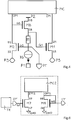
- the circuit of FIG. 2 comprises N-channel MOS transistors M1 and M2 having essentially the same threshold voltage and a current mirror MC having an input terminal IM and an output terminal OM. It has an output OT.
- the source terminals S1 and S2 of the transistors M1 and M2 are connected to a ground terminal GND while their drain terminals D1 and D2 are connected respectively to the terminals IM and OM and their gate terminals G1 and G2 are connected respectively to the positive and negative terminals of a voltage generator VG.
- the gate and drain terminals of the transistor M2 are connected together by means of a feedback path FP consisting of a short circuit.
- the output OT is connected to the terminal G2.
- FIG. 2 is also shown a very simple implementation of the mirror MC.
- This consists of two P-channel MOS transistors M3 and M4. Their source terminals are connected to a supply terminal VDD, their gate terminals are connected together, the drain terminal of the transistor M3 is connected to the terminal OM of the mirror MC and the drain terminal and the gate terminal of the transistor M4 are connected together to the terminal IM.
- the potential at the output OT is given by the sum of the threshold voltage of the transistors M1 and M2 and of the voltage of the generator VG multiplied by a constant as follows: A * K 2/ K 1 1- A * K 2/ K 1 where A is the current gain between input and output of the mirror MC, and K1 and K2 are the ratios W/L respectively of the transistors M1 and M2.
- This constant depends only on geometrical parameters and can thus be well controlled and made either very large or very small depending on requirements.
- this circuit is sized in such a way that the MOS transistors are operated normally under saturation conditions. It is recalled that in a first approximation the current of an MOS transistor in saturation does not depend on its voltage VDS.
- FIG. 3 shows a circuit analogous to that of FIG. 2 but based on two transistors M5 and M6, again of the MOS type but P channel. In this case the source terminals of the transistors are connected to a supply terminal VDD.
- FIG. 4 shows a variation of the circuit of FIG. 2 wherein in particular the path FP consists of a transistor and a two-terminal circuit element and the generator VG consists of the same two elements with the addition of a current generator.
- the path FP consists of a transistor and a two-terminal circuit element
- the generator VG consists of the same two elements with the addition of a current generator.
- P1, P2, P3 There are also shown by generalities three different potential references indicated by P1, P2, P3.
- the terminals S1 and S2 are connected to the third reference potential P3 which can coincide in a particular case with the ground terminal GND. If this potential does not coincide with the ground, a threshold subject to body effect will be extracted.
- the circuit comprises an N-channel MOS bias transistor MB having its drain terminal DB connected to the second reference potential P2, e.g. the supply terminal VDD, its gate terminal GB connected to the terminal OM and its source terminal SB connected to the terminal G1 and comprises a two-terminal circuit element B1 connected between the terminals G1 and G2 and a current generator IG connected between the terminal G2 and the first reference voltage P1, e.g. the ground terminal GND.
- the generator IG causes a constant current to flow in the transistor MB which holds it in saturation and in the two-terminal circuit element B1 which involves a constant potential difference between the terminals G1 and G2. Since the transistor MB is held in saturation the potentials of the terminals G2 and D2 are mutually interlocked.
- the two-terminal circuit element B1 can be provided by a resistor in a very simple manner or by diode-connected MOS transistors, by true diodes, etc..
- this circuit exhibits two work points, e.g. if the voltage falling at the ends of the two-terminal circuit element B1 is lower than the threshold. In these cases a start-up circuit is required to carry the circuit into the desired work point after starting. This is common practice in self-biasing circuits like this one.
- FIG. 1 shows a very advantageous variation of the circuit of FIG. 4 differentiated by the presence of a second two-terminal circuit element B2.
- This circuit also comprises a second two-terminal circuit element B2 essentially equal to the two-terminal circuit element B1 inserted between the terminal G2 and the generator IG.
- the output OT is connected to the node connecting the second two-terminal circuit element B2 and the generator IG.
- the generator IG causes the same current to flow both in the two-terminal circuit element B1 and the two-terminal circuit element B2 and, since these are essentially equal, at their ends is established essentially the same potential difference.
- the output is thus at a potential equal to the threshold of the transistors M1 and M2.
- Said threshold is extremely accurate because the effects of the two two-terminal circuit elements compensate for each other. In an integrated embodiment the technological and geometrical equality is relatively easy to provide.
- Said circuit can also be described differently by stating that it comprises a voltage divider VD having an intermediate output E3, a first terminal E1 and a second terminal E2 and consisting of two essentially equal two-terminal circuit elements B1 and B2 and stating that the output E3 is connected to the terminal G2, the terminal E1 is connected to the terminal G1 and to the terminal SB, and the terminal E2 is connected to the generator IG and the output OT.
- VD voltage divider VD having an intermediate output E3, a first terminal E1 and a second terminal E2 and consisting of two essentially equal two-terminal circuit elements B1 and B2 and stating that the output E3 is connected to the terminal G2, the terminal E1 is connected to the terminal G1 and to the terminal SB, and the terminal E2 is connected to the generator IG and the output OT.
- FIG. 6 A last circuit in accordance with the present invention is shown in FIG. 6.
- This consists of a threshold extractor circuit TE like one of those described above or even e.g. that of the known art shown in FIG.1 and of a stage having an input connected to the output OT and having an output UT of its own. This stage is identical to the extractor circuit of the known art shown in FIG. 1.
- This comprises two N-channel MOS transistors M7 and M8 having the same threshold voltage as that of the transistors M1 and M2 and another current mirror MC2 having an input terminal IM2 and an output terminal OM2.
- This is equipped with an input connected to the output OT and an output UT of its own.
- the source terminals S7 and S8 of the transistors M7 and M8 are connected to the ground terminal GND, their drain terminals D7 and D8 are respectively connected to the terminals IM2 and OM2, their gate terminals G7 and G8 are connected respectively to the input OT and the output UT.
- the gate and drain terminals of the transistor M8 are connected together.
- This new constant depends only on geometric parameters and can thus be controlled and made either much greater or much smaller than the old constant depending on requirements.
- the above described circuits serve to extract the threshold of N-channel MOS transistors. If it were necessary to extract the threshold of P-channel transistors it would be necessary to use dual circuits. Some examples of said duality are that the ground terminals GND must be replaced by supply terminals VDD, the supply terminals VDD by ground terminals GND, the N-channel transistors by P-channel transistors, the P-channel transistors by N-channel transistors, etc.
- the circuit of FIG. 3 is e.g. the dual (in the above sense) of the circuit of FIG. 2.
- the two transistors are applied two different and well controlled voltages.
- the present invention finds advantageous application in a circuit system for operation independently of temperature and/or dispersion of process parameters.
- Such a system comprises:
- bias network The purpose of such a bias network is to generate a bias current or voltage linked to the threshold of a reference element. Assuming that the threshold has a value which depends on a physical parameter and assuming that block operation also has an analogous dependence on the same parameter, by acting on the bias currents and/or voltages applied to the block in relation to the value of said threshold it is possible to compensate for the variations of said parameter (in time or from device to device) to achieve constant block operation.
Landscapes
- Engineering & Computer Science (AREA)
- Microelectronics & Electronic Packaging (AREA)
- Physics & Mathematics (AREA)
- Nonlinear Science (AREA)
- Electromagnetism (AREA)
- General Physics & Mathematics (AREA)
- Radar, Positioning & Navigation (AREA)
- Automation & Control Theory (AREA)
- Control Of Electrical Variables (AREA)
- Amplifiers (AREA)
Priority Applications (3)
| Application Number | Priority Date | Filing Date | Title |
|---|---|---|---|
| DE69434039T DE69434039T2 (de) | 1994-12-30 | 1994-12-30 | Verfahren zur Spannungschwelleextraktierung und Schaltung nach dem Verfahren |
| EP94830595A EP0720079B1 (fr) | 1994-12-30 | 1994-12-30 | Méthode d'extraction de la tension de seuil et circuit la mettant en oeuvre |
| US08/575,690 US5672960A (en) | 1994-12-30 | 1995-12-19 | Threshold extracting method and circuit using the same |
Applications Claiming Priority (1)
| Application Number | Priority Date | Filing Date | Title |
|---|---|---|---|
| EP94830595A EP0720079B1 (fr) | 1994-12-30 | 1994-12-30 | Méthode d'extraction de la tension de seuil et circuit la mettant en oeuvre |
Publications (2)
| Publication Number | Publication Date |
|---|---|
| EP0720079A1 true EP0720079A1 (fr) | 1996-07-03 |
| EP0720079B1 EP0720079B1 (fr) | 2004-09-29 |
Family
ID=8218606
Family Applications (1)
| Application Number | Title | Priority Date | Filing Date |
|---|---|---|---|
| EP94830595A Expired - Lifetime EP0720079B1 (fr) | 1994-12-30 | 1994-12-30 | Méthode d'extraction de la tension de seuil et circuit la mettant en oeuvre |
Country Status (3)
| Country | Link |
|---|---|
| US (1) | US5672960A (fr) |
| EP (1) | EP0720079B1 (fr) |
| DE (1) | DE69434039T2 (fr) |
Cited By (2)
| Publication number | Priority date | Publication date | Assignee | Title |
|---|---|---|---|---|
| CN103576065A (zh) * | 2012-07-24 | 2014-02-12 | 中芯国际集成电路制造(上海)有限公司 | 一种晶体管阈值电压的测试电路 |
| CN103675636A (zh) * | 2012-09-20 | 2014-03-26 | 中芯国际集成电路制造(上海)有限公司 | 一种晶体管阈值电压的测试电路 |
Families Citing this family (10)
| Publication number | Priority date | Publication date | Assignee | Title |
|---|---|---|---|---|
| EP0720078B1 (fr) * | 1994-12-30 | 1999-04-28 | Co.Ri.M.Me. | Méthode d'extraction de la tension de seuil et circuit la mettant en oeuvre |
| US6323725B1 (en) * | 1999-03-31 | 2001-11-27 | Qualcomm Incorporated | Constant transconductance bias circuit having body effect cancellation circuitry |
| EP1178383B1 (fr) * | 2000-08-03 | 2012-10-03 | STMicroelectronics Srl | Circuit pour générer un signal de tension insensible aux variations de température et peu sensible aux variations des variables de fabrication |
| US6489827B1 (en) * | 2000-10-30 | 2002-12-03 | Marvell International, Ltd. | Reduction of offset voltage in current mirror circuit |
| US6452454B1 (en) * | 2000-11-13 | 2002-09-17 | Conexant Systems, Inc. | Temperature compensation module |
| US6806762B2 (en) * | 2001-10-15 | 2004-10-19 | Texas Instruments Incorporated | Circuit and method to facilitate threshold voltage extraction and facilitate operation of a capacitor multiplier |
| US7215185B2 (en) * | 2005-05-26 | 2007-05-08 | Texas Instruments Incorporated | Threshold voltage extraction for producing a ramp signal with reduced process sensitivity |
| US7696826B2 (en) * | 2006-12-04 | 2010-04-13 | Skyworks Solutions, Inc. | Temperature compensation of collector-voltage control RF amplifiers |
| US8082796B1 (en) | 2008-01-28 | 2011-12-27 | Silicon Microstructures, Inc. | Temperature extraction from a pressure sensor |
| US8004350B2 (en) * | 2009-06-03 | 2011-08-23 | Infineon Technologies Ag | Impedance transformation with transistor circuits |
Citations (4)
| Publication number | Priority date | Publication date | Assignee | Title |
|---|---|---|---|---|
| US3823332A (en) * | 1970-01-30 | 1974-07-09 | Rca Corp | Mos fet reference voltage supply |
| GB2071955A (en) * | 1980-03-17 | 1981-09-23 | Philips Nv | Field-effect transistor current stabilizer |
| EP0397408A1 (fr) * | 1989-05-09 | 1990-11-14 | Advanced Micro Devices, Inc. | Générateur de tension de référence |
| EP0610064A2 (fr) * | 1993-02-01 | 1994-08-10 | STMicroelectronics Limited | Commutation à transistor |
Family Cites Families (5)
| Publication number | Priority date | Publication date | Assignee | Title |
|---|---|---|---|---|
| DE3545039A1 (de) * | 1985-12-19 | 1987-07-02 | Sgs Halbleiterbauelemente Gmbh | Spannungsbegrenzungsschaltung |
| JPH0666600B2 (ja) * | 1989-10-02 | 1994-08-24 | 株式会社東芝 | 電流検出回路 |
| EP0561469A3 (fr) * | 1992-03-18 | 1993-10-06 | National Semiconductor Corporation | Miroir de courant en cascade du type à enrichissement/appauvrissement |
| FR2703856B1 (fr) * | 1993-04-09 | 1995-06-30 | Sgs Thomson Microelectronics | Architecture d'amplificateur et application a un generateur de tension de bande interdite . |
| US5349286A (en) * | 1993-06-18 | 1994-09-20 | Texas Instruments Incorporated | Compensation for low gain bipolar transistors in voltage and current reference circuits |
-
1994
- 1994-12-30 DE DE69434039T patent/DE69434039T2/de not_active Expired - Fee Related
- 1994-12-30 EP EP94830595A patent/EP0720079B1/fr not_active Expired - Lifetime
-
1995
- 1995-12-19 US US08/575,690 patent/US5672960A/en not_active Expired - Lifetime
Patent Citations (4)
| Publication number | Priority date | Publication date | Assignee | Title |
|---|---|---|---|---|
| US3823332A (en) * | 1970-01-30 | 1974-07-09 | Rca Corp | Mos fet reference voltage supply |
| GB2071955A (en) * | 1980-03-17 | 1981-09-23 | Philips Nv | Field-effect transistor current stabilizer |
| EP0397408A1 (fr) * | 1989-05-09 | 1990-11-14 | Advanced Micro Devices, Inc. | Générateur de tension de référence |
| EP0610064A2 (fr) * | 1993-02-01 | 1994-08-10 | STMicroelectronics Limited | Commutation à transistor |
Non-Patent Citations (3)
| Title |
|---|
| SANSEN ET AL.: "A CMOS temperature-compensated Current Reference.", IEEE JOURNAL OF SOLID-STATE CIRCUITS, vol. 23, no. 3, NEW YORK US, pages 821 - 824, XP001397601 * |
| Y:P: TSIVIDIS ET AL.: "Threshold voltage generation and supply-independent biasing in c.m.o.s. integrated circuits.", IEE PROCEEDINGS G ELECTRONIC CIRCUITS & SYSTEMS., vol. 3, no. 1, STEVENAGE GB, pages 1 - 4, XP001405477 * |
| ZHENHUA WANG: "Automatic Vt extractors based on a ..... and their application.", IEEE JOURNAL OF SOLID-STATE CIRCUITS, vol. 27, no. 9, pages 1277 - 1285 * |
Cited By (2)
| Publication number | Priority date | Publication date | Assignee | Title |
|---|---|---|---|---|
| CN103576065A (zh) * | 2012-07-24 | 2014-02-12 | 中芯国际集成电路制造(上海)有限公司 | 一种晶体管阈值电压的测试电路 |
| CN103675636A (zh) * | 2012-09-20 | 2014-03-26 | 中芯国际集成电路制造(上海)有限公司 | 一种晶体管阈值电压的测试电路 |
Also Published As
| Publication number | Publication date |
|---|---|
| US5672960A (en) | 1997-09-30 |
| DE69434039D1 (de) | 2004-11-04 |
| EP0720079B1 (fr) | 2004-09-29 |
| DE69434039T2 (de) | 2006-02-23 |
Similar Documents
| Publication | Publication Date | Title |
|---|---|---|
| EP0194031B1 (fr) | Circuit CMOS de tension de référence de bande interdite | |
| US5357149A (en) | Temperature sensor circuit and constant-current circuit | |
| EP0720079B1 (fr) | Méthode d'extraction de la tension de seuil et circuit la mettant en oeuvre | |
| US4464588A (en) | Temperature stable CMOS voltage reference | |
| US4935690A (en) | CMOS compatible bandgap voltage reference | |
| EP0601540A1 (fr) | Générateur de tension de référence du type régulateur bandgap utilisé dans des circuits de transistors CMOS | |
| GB2290642A (en) | Operational transconductance amplifier and MOS multiplier | |
| US6057727A (en) | Accurate constant current generator | |
| US6111397A (en) | Temperature-compensated reference voltage generator and method therefor | |
| US6124704A (en) | Reference voltage source with temperature-compensated output reference voltage | |
| US5099205A (en) | Balanced cascode current mirror | |
| US4628280A (en) | Amplifier arrangement | |
| EP0301184B1 (fr) | Générateur de tension de référence CMOS | |
| US5083079A (en) | Current regulator, threshold voltage generator | |
| US5043652A (en) | Differential voltage to differential current conversion circuit having linear output | |
| US5703477A (en) | Current driver circuit with transverse current regulation | |
| US5459427A (en) | DC level shifting circuit for analog circuits | |
| US5952874A (en) | Threshold extracting method and circuit using the same | |
| US5656964A (en) | CMOS low-voltage four-quadrant multiplier | |
| EP0397408A1 (fr) | Générateur de tension de référence | |
| EP0019279B1 (fr) | Circuit comparateur de tension | |
| US6040720A (en) | Resistorless low-current CMOS voltage reference generator | |
| EP0725328A1 (fr) | Méthode pour changer le niveau de tension et circuit correspondant | |
| EP0655669B1 (fr) | Circuit de génération de tension de référence stable | |
| US4333025A (en) | N-Channel MOS comparator |
Legal Events
| Date | Code | Title | Description |
|---|---|---|---|
| PUAI | Public reference made under article 153(3) epc to a published international application that has entered the european phase |
Free format text: ORIGINAL CODE: 0009012 |
|
| AK | Designated contracting states |
Kind code of ref document: A1 Designated state(s): DE FR GB IT |
|
| 17P | Request for examination filed |
Effective date: 19961231 |
|
| 17Q | First examination report despatched |
Effective date: 19970206 |
|
| GRAP | Despatch of communication of intention to grant a patent |
Free format text: ORIGINAL CODE: EPIDOSNIGR1 |
|
| GRAS | Grant fee paid |
Free format text: ORIGINAL CODE: EPIDOSNIGR3 |
|
| GRAA | (expected) grant |
Free format text: ORIGINAL CODE: 0009210 |
|
| AK | Designated contracting states |
Kind code of ref document: B1 Designated state(s): DE FR GB IT |
|
| REG | Reference to a national code |
Ref country code: GB Ref legal event code: FG4D |
|
| REF | Corresponds to: |
Ref document number: 69434039 Country of ref document: DE Date of ref document: 20041104 Kind code of ref document: P |
|
| PGFP | Annual fee paid to national office [announced via postgrant information from national office to epo] |
Ref country code: DE Payment date: 20041125 Year of fee payment: 11 |
|
| ET | Fr: translation filed | ||
| PLBE | No opposition filed within time limit |
Free format text: ORIGINAL CODE: 0009261 |
|
| STAA | Information on the status of an ep patent application or granted ep patent |
Free format text: STATUS: NO OPPOSITION FILED WITHIN TIME LIMIT |
|
| 26N | No opposition filed |
Effective date: 20050630 |
|
| PGFP | Annual fee paid to national office [announced via postgrant information from national office to epo] |
Ref country code: GB Payment date: 20051125 Year of fee payment: 12 |
|
| PGFP | Annual fee paid to national office [announced via postgrant information from national office to epo] |
Ref country code: FR Payment date: 20051228 Year of fee payment: 12 |
|
| PG25 | Lapsed in a contracting state [announced via postgrant information from national office to epo] |
Ref country code: IT Free format text: LAPSE BECAUSE OF NON-PAYMENT OF DUE FEES;WARNING: LAPSES OF ITALIAN PATENTS WITH EFFECTIVE DATE BEFORE 2007 MAY HAVE OCCURRED AT ANY TIME BEFORE 2007. THE CORRECT EFFECTIVE DATE MAY BE DIFFERENT FROM THE ONE RECORDED. Effective date: 20051230 |
|
| PG25 | Lapsed in a contracting state [announced via postgrant information from national office to epo] |
Ref country code: DE Free format text: LAPSE BECAUSE OF NON-PAYMENT OF DUE FEES Effective date: 20060701 |
|
| GBPC | Gb: european patent ceased through non-payment of renewal fee |
Effective date: 20061230 |
|
| REG | Reference to a national code |
Ref country code: FR Ref legal event code: ST Effective date: 20070831 |
|
| PG25 | Lapsed in a contracting state [announced via postgrant information from national office to epo] |
Ref country code: GB Free format text: LAPSE BECAUSE OF NON-PAYMENT OF DUE FEES Effective date: 20061230 |
|
| PG25 | Lapsed in a contracting state [announced via postgrant information from national office to epo] |
Ref country code: FR Free format text: LAPSE BECAUSE OF NON-PAYMENT OF DUE FEES Effective date: 20070102 |