EP0720097A2 - Méthode pour l'identification de défauts non testables et redondants de circuits logiques séquentiels - Google Patents
Méthode pour l'identification de défauts non testables et redondants de circuits logiques séquentiels Download PDFInfo
- Publication number
- EP0720097A2 EP0720097A2 EP95308960A EP95308960A EP0720097A2 EP 0720097 A2 EP0720097 A2 EP 0720097A2 EP 95308960 A EP95308960 A EP 95308960A EP 95308960 A EP95308960 A EP 95308960A EP 0720097 A2 EP0720097 A2 EP 0720097A2
- Authority
- EP
- European Patent Office
- Prior art keywords
- circuit
- faults
- logic
- time frame
- leads
- Prior art date
- Legal status (The legal status is an assumption and is not a legal conclusion. Google has not performed a legal analysis and makes no representation as to the accuracy of the status listed.)
- Withdrawn
Links
Images



Classifications
-
- G—PHYSICS
- G01—MEASURING; TESTING
- G01R—MEASURING ELECTRIC VARIABLES; MEASURING MAGNETIC VARIABLES
- G01R31/00—Arrangements for testing electric properties; Arrangements for locating electric faults; Arrangements for electrical testing characterised by what is being tested not provided for elsewhere
- G01R31/28—Testing of electronic circuits, e.g. by signal tracer
- G01R31/317—Testing of digital circuits
- G01R31/3181—Functional testing
- G01R31/3183—Generation of test inputs, e.g. test vectors, patterns or sequences
- G01R31/318371—Methodologies therefor, e.g. algorithms, procedures
-
- G—PHYSICS
- G01—MEASURING; TESTING
- G01R—MEASURING ELECTRIC VARIABLES; MEASURING MAGNETIC VARIABLES
- G01R31/00—Arrangements for testing electric properties; Arrangements for locating electric faults; Arrangements for electrical testing characterised by what is being tested not provided for elsewhere
- G01R31/28—Testing of electronic circuits, e.g. by signal tracer
- G01R31/317—Testing of digital circuits
- G01R31/3181—Functional testing
- G01R31/3183—Generation of test inputs, e.g. test vectors, patterns or sequences
- G01R31/318342—Generation of test inputs, e.g. test vectors, patterns or sequences by preliminary fault modelling, e.g. analysis, simulation
-
- G—PHYSICS
- G01—MEASURING; TESTING
- G01R—MEASURING ELECTRIC VARIABLES; MEASURING MAGNETIC VARIABLES
- G01R31/00—Arrangements for testing electric properties; Arrangements for locating electric faults; Arrangements for electrical testing characterised by what is being tested not provided for elsewhere
- G01R31/28—Testing of electronic circuits, e.g. by signal tracer
- G01R31/317—Testing of digital circuits
- G01R31/3181—Functional testing
- G01R31/3185—Reconfiguring for testing, e.g. LSSD, partitioning
- G01R31/318533—Reconfiguring for testing, e.g. LSSD, partitioning using scanning techniques, e.g. LSSD, Boundary Scan, JTAG
- G01R31/318583—Design for test
- G01R31/318586—Design for test with partial scan or non-scannable parts
Definitions
- the present invention relates generally to the field of automatic test generation (ATG) for sequential digital logic circuits and more particularly to the identification of redundant and untestable faults in such circuits.
- ATG automatic test generation
- ATG automatic test generation
- the ATG system then automatically generates circuit stimuli which, when applied to the primary inputs of a fabricated instance of the given circuit design, will result in a response at the circuit's primary outputs which will identify (with a reasonable degree of certainty) whether the fabricated circuit is operating in accordance with the given circuit design.
- ATG systems typically perform their task (and measure the quality of their result) based on a fault "model” in which only a comparatively small number of possible malfunctions are considered.
- the most common such model the "stuck-at” fault model, enumerates the set of malfunctions in which each circuit lead ( i.e ., each input to and each output from a circuit element) may be individually “stuck” at one of its possible values ( e.g ., logic 0 or logic 1). In this manner, the number of possible faults to be considered is limited to twice the number of circuit leads.
- the "stuck-at" fault model has become well accepted as providing a reasonable correspondence to the set of likely physical errors which typically result from the fabrication process.
- circuit stimuli which will be able to "detect” that fault. That is, the system's goal is to find circuit stimuli which, when applied to the primary inputs of a "defective" circuit (i.e ., one which has the given fault), will result in a response at the circuit's primary outputs which differs from that of a properly operational circuit.
- these circuit stimuli are generated as a result of an exhaustive search procedure involving substantial trial and error. For most typical circuit designs, however, quite a few of the faults may, if actually present in a fabricated instance of the circuit, cause no discernable change in the circuit behavior at all.
- a method of identifying redundant and untestable faults in a sequential logic circuit is provided. Specifically, a lead in the circuit is selected and the circuit is analyzed to determine which faults would be hypothetically undetectable at a given time frame if the selected circuit lead were unable to assume a first value (e.g ., a logic 0) at a starting time frame, and which faults would be hypothetically undetectable at the given time frame if the selected circuit lead were unable to assume a second value (e.g ., a logic 1) at the starting time frame. Then, faults that would be undetectable at the given time frame in both hypothetical cases are identified as redundant and untestable faults.
- the above analysis may advantageously be repeated for each of a plurality of time frames in a range of time frames including a starting time frame.
- the time frames may, for example, comprise the blocks of a conventional combinational iterative array circuit model of the sequential logic circuit.
- the selected circuit lead may, for example, be a circuit line stem (e.g ., a fanout point) or a reconvergent input of a reconvergent circuit element (e.g ., gate).
- a circuit line stem e.g ., a fanout point
- a reconvergent input of a reconvergent circuit element e.g ., gate
- the method of the present invention may be repeated for each such circuit line stem and each such reconvergent input of a reconvergent gate in order to identify most, if not all, of the untestable faults for the given logic circuit.
- the faults which would be hypothetically undetectable at a given time frame if the selected lead were unable to assume a given one of the first and second values at a starting time frame may be determined based on a sequential implication procedure.
- This implication procedure comprises the propagation of uncontrollability indicators and the backward propagation of unobservability indicators.
- an uncontrollability indicator for the given (first or second) value is assigned to the selected circuit lead and is propagated through the circuit and/or through a range of time frames according to a predetermined set of propagation rules.
- unobservability indicators are generated in the circuit at various time frames based on the uncontrollability indicators, and these unobservability indicators are then propagated backward through the circuit and/or backward through the range of time frames, also in accordance with a predetermined set of propagation rules.
- the hypothetically undetectable faults are then determined based on the resultant indicators and their corresponding circuit leads and associated time frames.
- a sequential logic circuit design may be modified to remove logical redundancy.
- the method of the present invention is used to identify a redundant and untestable fault, and a portion of the circuit is removed based on the identified fault.
- Fig. 1 shows an illustrative testing process for a logic circuit, the test having been generated by an illustrative embodiment of the method of the present invention.
- Fig. 2 shows an example combinational circuit having untestable faults.
- Fig. 3 shows a flowchart describing an illustrative method for identifying untestable faults in a combinational circuit.
- Fig. 4 shows selected illustrative rules for propagation of uncontrollability indicators and generation and backward propagation of unobservability indicators.
- Fig. 5 shows a flowchart of an illustrative implication procedure for use in the illustrative procedure of Fig. 3.
- Fig. 6 shows an example sequential circuit having untestable faults.
- Fig. 7 illustrates a plurality of time frames through which an untestable fault analysis of a sequential circuit may be performed.
- Fig. 8 shows a flowchart describing an illustrative embodiment of the method of the present invention for identifying untestable faults in sequential circuits.
- Fig. 9 shows illustrative rules for propagation of uncontrollability indicators and backward propagation of unobservability indicators through flip-flop circuit elements and across time frames.
- Fig. 10 shows a flowchart of an illustrative sequential implication procedure for use in the illustrative procedure of Fig. 8.
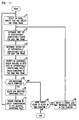
- Fig. 11 shows a flowchart describing an additional illustrative embodiment of the method of the present invention wherein redundancy may be eliminated from a sequential circuit.
- Fig. 1 shows an illustrative testing process for a logic circuit, the test having been generated by an illustrative embodiment of the method of the present invention.
- test generator 11 generates input stimuli and a corresponding expected output response based on a circuit description of the circuit to be tested.
- test generator 11 operates in accordance with an illustrative embodiment of the method of the present invention, as shown, for example, in Fig. 9, below.
- Test generator 11 may, for example, comprise a general purpose computer system and software executing thereon.
- Each fabricated instance of circuit 12 comprises a plurality of interconnected circuit elements 13 (e.g ., gates and flip-flops), one or more primary inputs 14 and one or more primary outputs 15 .
- ATE Automatic Test Equipment
- a typical ATE system comprises hardware components (in addition to the controlling computer) which are adapted to apply stimuli to a fabricated instance of a circuit, measure the responses from the fabricated instance of the circuit, and compare the measured response to a predetermined expected response.
- the fabricated instance of the circuit to be tested is usually "plugged into” the ATE system by means of a standardized interface.
- Fig. 2 illustrates an example combinational circuit having untestable faults.
- the example circuit comprises "And" gates 21 , 22 and 23 and "Or” gate 24 interconnected to each other and to primary inputs a , b and c and to primary output g .
- the fault f stuck-at-0 where the first input lead to "Or” gate 24 is permanently fixed to a logic 0 value.
- the first input lead to "Or” gate 24 is permanently fixed to a logic 0 value.
- a stuck-at fault e.g ., a stuck-at-0
- the given lead be "activated” to create a difference in value (e.g ., 0 vs . 1) between the faulty circuit and the properly operational circuit, and, furthermore, that the resultant difference in value be "propagated” to a primary output of the circuit where it can be observed by the testing process.
- the circuit lead In order to activate a stuck-at fault on a given circuit lead, it is merely necessary to set the circuit lead to a logic value opposite to the stuck-at value. For example, the lead must be set to a logic 1 in order to detect a stuck-at-0 fault.
- circuit leads c and d be set to a logic 1
- both circuit leads a and b be set to a logic 1.
- circuit lead e in order to propagate the f stuck-at-0 fault effect from f to a primary output, circuit lead e must be set to a logic 0 (since only when lead e is a logic 0 will "Or" gate 24 be sensitized to allow the logic value on lead f to propagate to primary output g ).
- at least one of circuit leads a and b must be set to a logic 0!
- Fig. 3 shows a flowchart describing an illustrative method for detecting untestable faults in combinational circuits such as the example circuit of Fig. 2.
- the illustrative procedure iteratively selects each of a plurality of the circuit leads in the circuit in turn.
- the procedure begins in step 31 by selecting one such (not previously selected) circuit lead for analysis.
- the selected leads may be limited to stems of circuit lines having reconvergent fanout (i.e ., the outputs of gates which have fanout branches which proceed along paths that ultimately reconverge as inputs to another gate) and to reconvergent inputs of reconvergent gates, rather than selecting each and every circuit lead in the circuit in turn.
- the selected leads are limited to only circuit line stems.
- some of the untestable faults in a given circuit may not be identified. Nonetheless, such a limited approach typically identifies most of the untestable faults which would be identified by including the analysis of reconvergent inputs, while a significant reduction in computation time is achieved by analyzing only circuit line stems.
- step 32 of the illustrative procedure of Fig. 3 "marks" that circuit lead as being (hypothetically) uncontrollable to a logic 0 ( i.e ., unable to assume a logic 0 value, regardless of the values applied to the primary inputs of the circuit).
- step 33 an implication procedure is applied which marks other circuit nodes as uncontrollable to an appropriate logic value or unobservable ( i.e ., unable to have its value propagated to a primary output) as appropriate by implication from the originally hypothesized uncontrollability condition.
- a first set of hypothetically untestable faults may be deduced. (See discussion of the implication rules shown in Fig. 4 and discussion of the implication procedure of Fig. 5 below.)
- step 34 marks the selected circuit lead as being (hypothetically) uncontrollable to a logic 1 (i.e ., unable to assume a logic 1 value).
- step 35 the implication procedure is again applied, thereby marking other circuit nodes as uncontrollable to an appropriate logic value or unobservable as appropriate by implication from the originally hypothesized uncontrollability condition. Based on this set of resultant uncontrollability and unobservability indicators, a second set of hypothetically untestable faults may be deduced.
- Decisio n 37 determines if there are more circuit leads to select (e.g ., whether all stems of circuit lines having reconvergent fanout and all reconvergent inputs of reconvergent gates have been analyzed) and repeats the above described procedure if there are more such leads to be analyzed. If there are no more circuit leads to analyze, step 38 performs the automatic test generation (ATG) process on the circuit, explicitly excluding those faults which have been identified as untestable by the procedure of steps 31 through 37 . As described above, the ATG process of step 38 produces circuit stimuli and expected output responses.
- ATG automatic test generation
- Fig. 4 shows certain illustrative rules for the propagation of uncontrollability indicators and backward propagation of unobservability indicators. These rules may be used by the illustrative implication procedure used in the procedure of Fig. 3 and shown in more detail in Fig. 5. Gates 41 , 42 and 43 and circuit line fanout point 44 illustrate rules for the propagation of uncontrollability indicators, and gates 45 , 46 and 47 illustrate rules for backward propagation of unobservability indicators. By convention, “ 0 ⁇ " will be used to denote the status of a circuit lead that is (hypothesized to be) uncontrollable to the logic value 0.
- Inverter gate 41 shows that when an inverter gate's input is marked with a " 0 ⁇ ,” its output may be marked with a " 1 ⁇ .” Similarly, when an inverter gate's input is marked with a “ 1 ⁇ ,” its output may be marked with a " 0 ⁇ .” Moreover, when an inverter gate's output is marked with a " 0 ⁇ ,” its input may be marked with a " 1 ⁇ ,” and when an inverter gate's output is marked with a " 1 ⁇ ,” its input may be marked with a " 0 ⁇ .” These rules result from the obvious fact that if an inverter's input cannot be set to a given value, its output cannot be set to the opposite value, and vice versa .
- "Nand” gate 42 shows that when all of a "Nand” gate's inputs are marked with a “ 0 ⁇ ,” its output may be marked with a “ 1 ⁇ ,” since if none of a “Nand” gate's inputs can be set to a logic 0, there is no way to set its output to a logic 1. Moreover, when a "Nand” gate's output is marked with a “ 1 ⁇ ,” all of its inputs may be marked with a " 0 ⁇ ,” since if a "Nand” gate's output cannot be set to a logic 1, there must be no way to set any of its inputs to a logic 0.
- "Nand” gate 43 shows that when any of a "Nand” gate's inputs are marked with a “ 1 ⁇ ,” its output may be marked with a " 0 ⁇ ,” since if any of a "Nand” gate's inputs cannot be set to a logic 1, there is no way to set its output to a logic 0.
- fanout point 44 shows that when a circuit line stem is marked with a " 0 ⁇ ,” each of its fanout branches may be marked with a " 0 ⁇ ,” and, similarly, when a circuit line stem is marked with a “ 1 ⁇ ,” each of its fanout branches may be marked with a " 1 ⁇ ,” since a fanout branch can only be set to a given value by setting its corresponding stem to that value. Moreover, when each fanout branch of a circuit line stem is marked with a " 0 ⁇ ,” the stem may be marked with a " 0 ⁇ ,” and, similarly, when each fanout branch is marked with a " 1 ⁇ ,” the stem may be marked with a " 1 ⁇ ,” for the same reason. Similar rules for the propagation of uncontrollability indicators which may be applied to other gate types or combinational circuit elements will be obvious to those skilled in the art.
- Inverter gate 45 shows that when an inverter gate's output is marked with a "*,” its input may also be marked with a "*.”
- “Nand” gate 46 shows that when a "Nand” gate's output is marked with a "*,” each of its inputs may be marked with a “*.” These rules result from the fact that if any gate's output cannot be observed, none of its inputs can be observed.
- "Nand” gate 47 shows that when one of its inputs is marked with a " 1 ⁇ ,” each of its other inputs may be marked with a "*,” since an input to a "Nand” gate can only be observed by setting all of the other inputs to a logic 1.
- Fig. 5 shows a flowchart of an illustrative implication procedure for use in steps 33 and 35 of the illustrative procedure of Fig. 3. Specifically, the procedure of Fig. 5 determines a set of faults that would (hypothetically) be untestable if a given, selected circuit lead were uncontrollable to a specified value. This illustrative procedure may, for example, use propagation rules such as those shown in Fig. 4 and described above.
- Step 51 assigns an initial uncontrollability indicator to the selected circuit lead.
- This uncontrollability indicator marks the selected lead as uncontrollable to the specified logic value (0 or 1) depending on whether the procedure is being used to implement step 33 or step 35 of the procedure of Fig. 3.
- step 52 uses predetermined uncontrollability indicator propagation rules (such as those shown on gates 41 , 42 and 43 and circuit line fanout point 44 in Fig. 4) to propagate uncontrollability indicators through the circuit.
- Step 53 uses predetermined unobservability indicator creation rules (such as that shown on gate 47 in Fig. 4) to assign initial unobservability indicators to appropriate circuit leads.
- Step 54 then uses predetermined unobservability indicator propagation rules (such as those shown on gates 45 and 46 in Fig. 4) to propagate unobservability indicators backward through the circuit.
- step 55 of the procedure of Fig. 5 chooses each circuit lead which has been marked with an uncontrollability indicator and, depending on the uncontrollability value with which it has been marked (as determined by decision 56 ), either the stuck-at-1 fault on that circuit lead (step 57 ) or the stuck-at-0 fault on that circuit lead (step 58 ) is added to the set of hypothetically untestable faults.
- Decision 59 returns to step 55 to choose another such circuit lead until each uncontrollabilty indicator has been processed.
- step 61 chooses each circuit lead which has been marked with an unobservability indicator, and step 62 adds both the stuck-at-0 fault and the stuck-at-1 fault on that circuit lead to the set of hypothetically untestable faults. Decision 63 returns to step 61 to choose another such circuit lead until each unobservability indicator has been processed.
- FIG. 6 shows an example sequential circuit having untestable faults.
- the example circuit comprises "Or” gates 64 and 69 , "And” gate 66 and “Flip-flop” elements 65 , 67 and 68 interconnected to each other and to primary inputs a , b and c and to primary output i .
- "Flip-flops" 65 , 67 and 68 are controlled by a common clock signal, CLK , as is typical for synchronous sequential circuits.
- each lead in the circuit can (at least in theory) assume a distinct logic value at each time frame. However, in a synchronous sequential circuit, only one such (stable) logic value may be assumed by a given circuit lead at each time frame. Thus, if the detection of a given fault requires that some circuit lead assume contradictory logic values at the same time frame , the fault is necessarily undetectable.
- circuit lead g In order to "activate” this fault at a given time frame (call it time “t"), it is necessary that circuit lead g assume the logic 1 value at time “t.” This implies that circuit lead f is a logic 1 at the previous time frame ( i.e ., time "t-1") which, in turn, implies that both circuit leads e and c1 are logic 1 at time “t-1.” Therefore circuit lead c must be a logic 1 at time "t-1.” However, in order to propagate the fault g stuck-at-0, it is necessary that circuit lead h be a logic 0 at the time when the fault has been activated ( i.e ., time "t").
- circuit lead c2 be a logic 0 at the previous time frame (i.e ., time "t-1"). Therefore, circuit lead c must be a logic 0 at time "t-1,” contradicting the requirement that circuit lead c must be a logic 1 at time "t-1.”
- untestable faults may be identified in a synchronous sequential circuit by analyzing logic value assignments over a plurality of time frames.
- a fault can be determined to be untestable by performing such an analysis until a contradiction is reached.
- the above analysis of the example sequential circuit of Fig. 6 employed a procedure similar to that typically performed by ATG systems -- that is, such an analysis requires, in general, a time-consuming exhaustive search.
- a method of identifying untestable faults in a sequential circuit determines faults the detection of which would require a selected circuit lead to simultaneously ( i.e ., at the same time frame) assume two distinct logic values.
- This illustrative method selects a circuit lead for analysis, and defines an arbitrary time frame (referred to herein as the starting time frame or time "0") at which time it is presumed that a conflict of logic value assignment at that circuit lead may hypothetically occur.
- a predetermined range of time frames which includes the starting time frame is specified.
- Faults whose activation and/or propagation (at any one of these time frames) are determined to require such a conflict of assigned logic values on the selected lead at the starting time frame are identified.
- a fault whose activation and/or propagation at a given time frame requires such a conflict is said to be undetectable at the given time frame.
- the starting time frame is chosen arbitrarily (i.e ., the starting time frame can be any time frame), these faults are necessarily untestable.
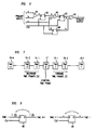
- Fig. 7 illustrates a plurality of time frames through which such an analysis of a sequential circuit may be performed.
- starting time frame 17 is identified as time "0," which represents the time frame at which conflicts are (hypothetically) presumed to occur.
- Forward time frames 18-1 through 18-f represent a predetermined number of relative time frames ("f" time frames identified as time frame “1” through time frame “f") immediately subsequent to the starting time frame.
- Backward time frames 19-1 through 19-b represent a predetermined number of relative time frames ("b" time frames identified as time frame “-1” through time frame "-b") immediately prior to the starting time frame.
- g stuck-at-0 requires a conflict on circuit lead c one time frame earlier than the time frame at which it is desired that the fault be activated and propagated.
- g stuck-at-0 is necessarily an untestable fault.
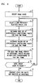
- Fig. 8 shows a flowchart describing an illustrative embodiment of the method of the present invention for identifying untestable faults in sequential circuits.
- step 71 specifies the time frame range for analysis. That is, a predetermined number of time frames subsequent to a starting time frame ("f") and a predetermined number of time frames prior to the starting time frame ("b"), such as is illustratively shown in Fig. 7, is specified.
- f a predetermined number of time frames subsequent to a starting time frame
- b predetermined number of time frames prior to the starting time frame
- predetermined numbers may be fixed at constant values (e.g ., five), or, in alternative embodiments, these numbers could be gradually increased while new untestable faults are found or until predefined maximum values (e.g ., five) are reached.
- Step 72 selects a (not previously selected) circuit lead for analysis.
- Step 73 determines a plurality of "first" sets of faults, one set for each of the "f+b+1" relative time frames, which would be (hypothetically) untestable if the selected circuit lead were uncontrollable to a logic 0 value at the starting time frame ( i.e ., time frame "0").
- step 74 determines a plurality of "second" sets of faults, one set for each of the "f+b+1" relative time frames, which would be (hypothetically) untestable if the selected circuit lead were uncontrollable to a logic 1 value at time frame "0."
- steps 73 and 74 each determine faults which either could not be activated at that time frame or, if activated, could not be propagated at that time frame, given the hypothetical assumption that the selected circuit lead cannot assume the corresponding logic value at time frame "0.”
- Step 75 then identifies as untestable the faults which are included in both the first and second sets of hypothetically untestable faults which correspond to the same (relative) time frame .
- step 77 performs the automatic test generation (ATG) process on the original sequential circuit, explicitly excluding those faults which have been identified as untestable by the procedure of steps 71 through 76 .
- ATG automatic test generation
- Steps 73 and 74 of the illustrative procedure of Fig. 8 may be performed with use of a sequential implication procedure which assigns uncontrollability and unobservability indicators to various circuit leads at the various time frames.
- a sequential implication procedure which assigns uncontrollability and unobservability indicators to various circuit leads at the various time frames.
- the implication procedure must handle flip-flop circuit elements and assign each of these indicators to specific time frames.
- a sequential implication procedure must be able to make such assignments across time frame boundaries.
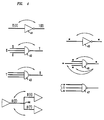
- Fig. 9 shows illustrative rules for propagation of uncontrollability indicators and backward propagation of unobservability indicators through flip-flop circuit elements.
- "Flip-flop” 48 shows that when a flip-flop's data input is marked with a " 0 ⁇ " at a given time frame ( e.g ., time "i"), its ("Q") output may be marked with a " 0 ⁇ " at the next time frame ( e.g ., time "i+1").
- flip-flop 49 shows that when a flip-flop's ("Q") output is marked with a "*" at a given time frame (e.g. , time “i"), its data input may be marked with a "*" at the previous time frame ( e.g ., time "i-1"). That is, if a flip-flop's output is unobservable at a given time frame, its data input is unobservable at the previous time frame.
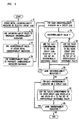
- Fig. 10 shows a flowchart of an illustrative sequential implication procedure for use in steps 73 and 74 of the illustrative procedure of Fig. 8. Specifically, the procedure of Fig. 10 determines, for each time frame in the time frame range, a set of faults that would (hypothetically) be undetectable at that time frame if a given, selected circuit lead were uncontrollable to a specified value at the starting time frame.
- This illustrative procedure may, for example, use propagation rules such as those shown in Figs. 4 and 9 and described above.
- Step 91 assigns an initial uncontrollability indicator to the selected circuit lead at the starting time frame (i.e ., time frame "0").
- This uncontrollability indicator marks the selected lead as uncontrollable to the specified logic value (0 or 1) depending on whether the procedure is being used to implement step 73 or step 74 of the procedure of Fig. 8.
- step 92 uses predetermined uncontrollability indicator propagation rules (such as those shown on gates 41 , 42 and 43 and circuit line fanout point 44 in Fig. 4, and on flip-flop 48 in Fig. 9) to propagate uncontrollability indicators through the circuit and across the various time frames within the time frame range. (Note that the propagation rule shown on flip-flop 48 in Fig.
- Step 93 uses predetermined unobservability indicator creation rules (such as that shown on gate 47 in Fig. 4) to assign initial unobservability indicators to appropriate circuit leads.
- Step 94 uses predetermined unobservability indicator propagation rules (such as those shown on gates 45 and 46 in Fig. 4 and on flip-flop 49 in Fig. 9) to propagate unobservability indicators backward through the circuit and backward across time frames within the time frame range. (Note that the propagation rule shown on flip-flop 49 in Fig. 9 will advantageously not be used if to do so would propagate an unobservability indicator to a time frame outside the time frame range.)
- step 95 selects, in turn, each of the time frames in the analyzed time frame range, and step 96 then chooses each circuit lead which has been marked with an uncontrollability indicator at that time frame. Then, depending on the uncontrollability value with which it has been marked (as determined by decision 97 ), either the stuck-at-1 fault on that circuit lead (step 98 ) or the stuck-at-0 fault on that circuit lead (step 99 ) is added to the set of hypothetically undetectable faults for the given time frame. Decision 100 returns to step 96 to choose another such circuit lead until each uncontrollabilty indicator for the given time frame has been processed.
- step 101 chooses each circuit lead which has been marked with an unobservability indicator at the given time frame, and step 62 adds both the stuck-at-0 fault and the stuck-at-1 fault on that circuit lead to the set of hypothetically undetectable faults for the given time frame.
- Decision 103 returns to step 101 to choose another such circuit lead until each unobservability indicator for the given time frame has been processed.
- decision 104 then returns to step 95 to process another time frame until all time frames in the time frame range have been processed, thereby producing a set of hypothetically undetectable faults for each time frame in the time frame range.
- Fig. 11 shows a flowchart describing an additional illustrative embodiment of the method of the present invention wherein redundancy may be eliminated from a sequential circuit. Since the method of the present invention identifies faults in a sequential circuit which are not only untestable but, in fact, redundant, a sequential circuit may be simplified in accordance with one illustrative embodiment of the method of the present invention by iteratively identifying untestable/redundant faults and reducing the circuit design in accordance therewith. The resultant circuit will be smaller, but logically equivalent to, the original circuit.
- the illustrative redundancy elimination procedure of Fig. 11 identifies one untestable fault (at a time), removes the redundant portion of the circuit implied by the untestability of that fault, and then iterates this process until no more untestable faults are identified.
- step 81 first selects for analysis an initial circuit lead from the given (current) version of the circuit and specifies a time frame range for analysis, thereby beginning a given iteration of the redundancy elimination procedure.
- Step 82 determines a plurality of first sets of hypothetically untestable faults, one set for each time frame, based on the assumption that the selected circuit lead could not, for example, be controlled to a logic 0 at the starting time frame.
- step 83 determines a plurality of second sets of hypothetically untestable faults, one set for each time frame, based on the assumption that the selected circuit lead could not, for example, be controlled to a logic 1 at the starting time frame.
- step 84 then identifies as untestable, faults included in both (first and second) sets of hypothetically untestable faults which correspond to the same time frame.
- Step 86 determines whether any faults have been identified as untestable in step 84 , and if so, step 86 selects any one of these identified untestable faults. Step 87 then removes the portion of the circuit which can be determined to be redundant based on the untestability of the selected fault. For example, if a stuck-at-0 fault on a given circuit lead is an untestable fault, then all circuitry which feeds into the given circuit lead may be removed (to the extent that it does not feed into any other circuit leads which are not being removed), and the given circuit lead may be affixed to a logic 0 value ( e.g ., tied to ground).
- a logic 0 value e.g ., tied to ground
- the selection of an untestable fault in step 86 may be made arbitrarily, or it may advantageously be based on the portion of the circuit that would be removed in step 87 based on its selection. (For example, untestable faults could advantageously be selected based on the quantity of circuitry that their selection would cause to be removed. In this manner, the efficiency of the redundancy elimination procedure may be improved.)
- the selected untestable fault may advantageously first be analyzed to ensure that the removal of the associated redundant circuitry will not result in an uninitializable circuit.
- This validation process may, for example, be carried out by checking the given node in each time frame to ensure that there is no time at which the node is uncontrollable to the faulty value.
- the circuit will not become uninitializable by the removal of the corresponding circuitry so long as node "n” does not appear as uncontrollable to a one in any of the time frames.
- step 87 After step 87 has removed the redundant circuitry, a new iteration of the redundancy elimination procedure begins by returning to step 81 .
- the new iteration will use the new version of the circuit as its current version.
- step 84 determines whether there are more circuit leads to be analyzed ( i.e ., selected) within the given iteration ( i.e ., since the circuit was last modified by step 87 ). If so, step 89 selects a circuit lead which has not yet been selected within the given iteration and returns to step 82 in a further attempt to identify untestable faults in the current version of the circuit. If decision 88 determines that there are no more circuit leads to be analyzed within the given iteration, then an entire iteration of the procedure has been performed without identifying any untestable faults -- that is, no untestable faults have been found in the current version of the circuit. Thus, the redundancy elimination procedure of Fig. 8 terminates, and the final version of the circuit may be adopted as logically equivalent to the original circuit design.
Landscapes
- Engineering & Computer Science (AREA)
- General Engineering & Computer Science (AREA)
- Physics & Mathematics (AREA)
- General Physics & Mathematics (AREA)
- Test And Diagnosis Of Digital Computers (AREA)
- Tests Of Electronic Circuits (AREA)
- For Increasing The Reliability Of Semiconductor Memories (AREA)
Applications Claiming Priority (2)
| Application Number | Priority Date | Filing Date | Title |
|---|---|---|---|
| US36607594A | 1994-12-29 | 1994-12-29 | |
| US366075 | 1994-12-29 |
Publications (2)
| Publication Number | Publication Date |
|---|---|
| EP0720097A2 true EP0720097A2 (fr) | 1996-07-03 |
| EP0720097A3 EP0720097A3 (fr) | 1998-10-14 |
Family
ID=23441565
Family Applications (1)
| Application Number | Title | Priority Date | Filing Date |
|---|---|---|---|
| EP95308960A Withdrawn EP0720097A3 (fr) | 1994-12-29 | 1995-12-11 | Méthode pour l'identification de défauts non testables et redondants de circuits logiques séquentiels |
Country Status (3)
| Country | Link |
|---|---|
| EP (1) | EP0720097A3 (fr) |
| JP (1) | JPH08304517A (fr) |
| CA (1) | CA2159036C (fr) |
Cited By (2)
| Publication number | Priority date | Publication date | Assignee | Title |
|---|---|---|---|---|
| FR2798472A1 (fr) * | 1999-09-15 | 2001-03-16 | Centre Nat Etd Spatiales | Procede de localisation d'elements defectueux dans un circuit integre |
| CN102770777A (zh) * | 2010-03-04 | 2012-11-07 | 罗伯特·博世有限公司 | 用于确定错误屏蔽因素的反向分析的改善 |
Family Cites Families (1)
| Publication number | Priority date | Publication date | Assignee | Title |
|---|---|---|---|---|
| JP2604606B2 (ja) * | 1987-11-24 | 1997-04-30 | 株式会社アドバンテスト | 回路試験装置 |
-
1995
- 1995-09-25 CA CA 2159036 patent/CA2159036C/fr not_active Expired - Fee Related
- 1995-12-11 EP EP95308960A patent/EP0720097A3/fr not_active Withdrawn
- 1995-12-26 JP JP7338407A patent/JPH08304517A/ja not_active Withdrawn
Cited By (5)
| Publication number | Priority date | Publication date | Assignee | Title |
|---|---|---|---|---|
| FR2798472A1 (fr) * | 1999-09-15 | 2001-03-16 | Centre Nat Etd Spatiales | Procede de localisation d'elements defectueux dans un circuit integre |
| WO2001020355A1 (fr) * | 1999-09-15 | 2001-03-22 | Centre National D'etudes Spatiales | Procede de localisation d'elements defectueux dans un circuit integre |
| US6526546B1 (en) | 1999-09-15 | 2003-02-25 | Centre National D'etudes Spatiales | Method for locating faulty elements in an integrated circuit |
| CN102770777A (zh) * | 2010-03-04 | 2012-11-07 | 罗伯特·博世有限公司 | 用于确定错误屏蔽因素的反向分析的改善 |
| CN102770777B (zh) * | 2010-03-04 | 2015-05-20 | 罗伯特·博世有限公司 | 用于确定错误屏蔽因素的反向分析的改善 |
Also Published As
| Publication number | Publication date |
|---|---|
| CA2159036A1 (fr) | 1996-06-30 |
| CA2159036C (fr) | 1999-01-26 |
| EP0720097A3 (fr) | 1998-10-14 |
| JPH08304517A (ja) | 1996-11-22 |
Similar Documents
| Publication | Publication Date | Title |
|---|---|---|
| US5043986A (en) | Method and integrated circuit adapted for partial scan testability | |
| US6868532B2 (en) | Method and program product for designing hierarchical circuit for quiescent current testing and circuit produced thereby | |
| Goel et al. | PODEM-X: An automatic test generation system for VLSI logic structures | |
| US6003150A (en) | Method for testing field programmable gate arrays | |
| US5132974A (en) | Method and apparatus for designing integrated circuits for testability | |
| US7661050B2 (en) | Method and system for formal verification of partial good self test fencing structures | |
| US6766473B2 (en) | Test pattern selection apparatus for selecting test pattern from a plurality of check patterns | |
| US5291495A (en) | Method for designing a scan path for a logic circuit and testing of the same | |
| US7039845B2 (en) | Method and apparatus for deriving a bounded set of path delay test patterns covering all transition faults | |
| EP0803814A1 (fr) | Testabilité améliorée par transformation d'horloge | |
| US5566187A (en) | Method for identifying untestable faults in logic circuits | |
| US10509072B2 (en) | Test application time reduction using capture-per-cycle test points | |
| US6862717B2 (en) | Method and program product for designing hierarchical circuit for quiescent current testing | |
| US5587919A (en) | Apparatus and method for logic optimization by redundancy addition and removal | |
| US6707313B1 (en) | Systems and methods for testing integrated circuits | |
| US6256770B1 (en) | Register transfer level (RTL) based scan insertion for integrated circuit design processes | |
| US7139948B2 (en) | Method for determining the impact on test coverage of scan chain parallelization by analysis of a test set for independently accessible flip-flops | |
| US20050102594A1 (en) | Method for test application and test content generation for AC faults in integrated circuits | |
| US7219287B1 (en) | Automated fault diagnosis in a programmable device | |
| US5559811A (en) | Method for identifying untestable and redundant faults in sequential logic circuits. | |
| US7900112B2 (en) | System and method for digital logic testing | |
| Cantoro et al. | A new technique to generate test sequences for reconfigurable scan networks | |
| US20020188904A1 (en) | Efficiency of fault simulation by logic backtracking | |
| EP0720097A2 (fr) | Méthode pour l'identification de défauts non testables et redondants de circuits logiques séquentiels | |
| US20170010325A1 (en) | Adaptive test time reduction |
Legal Events
| Date | Code | Title | Description |
|---|---|---|---|
| PUAI | Public reference made under article 153(3) epc to a published international application that has entered the european phase |
Free format text: ORIGINAL CODE: 0009012 |
|
| AK | Designated contracting states |
Kind code of ref document: A2 Designated state(s): DE FR GB |
|
| PUAL | Search report despatched |
Free format text: ORIGINAL CODE: 0009013 |
|
| AK | Designated contracting states |
Kind code of ref document: A3 Designated state(s): DE FR GB |
|
| 17P | Request for examination filed |
Effective date: 19990401 |
|
| STAA | Information on the status of an ep patent application or granted ep patent |
Free format text: STATUS: THE APPLICATION HAS BEEN WITHDRAWN |
|
| 18W | Application withdrawn |
Withdrawal date: 19990624 |