EP0720170A2 - Multiplicateur de tension amélioré et incorporé sur la puce pour mémoires à semi-conducteurs - Google Patents
Multiplicateur de tension amélioré et incorporé sur la puce pour mémoires à semi-conducteurs Download PDFInfo
- Publication number
- EP0720170A2 EP0720170A2 EP95830522A EP95830522A EP0720170A2 EP 0720170 A2 EP0720170 A2 EP 0720170A2 EP 95830522 A EP95830522 A EP 95830522A EP 95830522 A EP95830522 A EP 95830522A EP 0720170 A2 EP0720170 A2 EP 0720170A2
- Authority
- EP
- European Patent Office
- Prior art keywords
- capacitor
- voltage
- switches
- pin
- multiplier circuit
- Prior art date
- Legal status (The legal status is an assumption and is not a legal conclusion. Google has not performed a legal analysis and makes no representation as to the accuracy of the status listed.)
- Granted
Links
- 230000015654 memory Effects 0.000 title description 5
- 239000004065 semiconductor Substances 0.000 title description 2
- 239000003990 capacitor Substances 0.000 claims abstract description 53
- 239000000758 substrate Substances 0.000 claims description 2
- 230000003071 parasitic effect Effects 0.000 description 11
- 235000013599 spices Nutrition 0.000 description 11
- 238000004088 simulation Methods 0.000 description 8
- 238000010586 diagram Methods 0.000 description 6
- 238000000034 method Methods 0.000 description 6
- 238000013459 approach Methods 0.000 description 4
- 230000000694 effects Effects 0.000 description 4
- 238000007600 charging Methods 0.000 description 3
- 230000008878 coupling Effects 0.000 description 3
- 238000010168 coupling process Methods 0.000 description 3
- 238000005859 coupling reaction Methods 0.000 description 3
- 230000008569 process Effects 0.000 description 3
- 230000008859 change Effects 0.000 description 2
- 238000009792 diffusion process Methods 0.000 description 2
- 238000007599 discharging Methods 0.000 description 2
- 238000005516 engineering process Methods 0.000 description 2
- 230000009471 action Effects 0.000 description 1
- 238000010276 construction Methods 0.000 description 1
- 238000004870 electrical engineering Methods 0.000 description 1
- 238000007667 floating Methods 0.000 description 1
- 230000006870 function Effects 0.000 description 1
- 238000000926 separation method Methods 0.000 description 1
- 238000009966 trimming Methods 0.000 description 1
Images







Classifications
-
- G—PHYSICS
- G11—INFORMATION STORAGE
- G11C—STATIC STORES
- G11C5/00—Details of stores covered by group G11C11/00
- G11C5/14—Power supply arrangements, e.g. power down, chip selection or deselection, layout of wirings or power grids, or multiple supply levels
- G11C5/145—Applications of charge pumps; Boosted voltage circuits; Clamp circuits therefor
Definitions
- This invention broadly relates to semiconductor memories and, more particularly, it relates to a novel implementation of a voltage multiplier circuit which enables integrated circuits manufactured in CMOS technology to be operated with a conventional supply voltage of 3.3 volts or 5.0 volts also in all those case wherein within the circuit and in certain circumstances, higher voltages are required.
- the voltage multiplication efficiency and the load current drive capability are noticeably improved with respect to the prior art approaches, particularly with respect to the charge pumps. Since the multiplication efficiency is strictly related to the power efficiency, this technique is also suitable for low power applications.
- Formula (1) means that the multiplication efficiency and the power efficiency, that is the ratio between the output power and the total supplied power, express the same concept.
- the diodes are replaced by N-channel MOS transistors connected to operate as diodes.
- P-channel transistors are not used because of difficulties associated with the substrate bias and with turning the devices off. Due to the poor capability of the N-channel MOS transistors to efficiently switch high voltage levels, the multiplication efficiency and the load current drive capability are both noticeably degraded with respect to the diode implementation. For example, a typical MOS transistor charge pump implementation for generating a voltage of 18 volt from a 5 volt power supply has almost twice the stages needed for an equivalent diode implementation.
- a first aspect of this invention suggests a novel technique for realising a voltage multiplier circuit, a conceptual electric diagram together with its related timings is shown in Figure 2.
- Each capacitor Ci is charged to voltage Vdd directly by the power supply Vdd when switches Di and Si are on and switches Tj are off.
- switches Di and Si turn off and the switches Tj turn on.
- capacitors Ci are connected in series and are discharged directly to the output.
- the minimum number N of capacitors should be used to exceed, by a reasonable value ⁇ V, the desired output voltage Vout.
- ⁇ V Vdd * (N + 1) - Vout (4)
- Iout ⁇ V * C * F / N
- formula (1) is still valid. Since the value of N is equal, or almost equal, to the theoretical minimum value also in a practical implementation, the new voltage multiplier is suitable for low power applications, such as in circuits with battery power supplies.
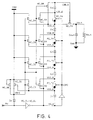
- FIG. 3 A first practical implementation of the conceptual scheme of Figure 2 is shown in Figure 3.
- a bootstrap technique has been used to properly drive the gates of the N-channel MOS transistors whose sources are not at Vss potential.
- capacitor Cb is inserted between the clock signal source PH and the gates of all transistors NC_Di while the diode transistor NC_B is inserted between said capacitor Cb and the voltage supply Vdd.
- the circuit can be ideally considered as divided into stages the components of which are all connected in analogous way.
- transistor PC_T1 is inserted between voltage Vdd and node V10 for coupling or connection to a first terminal (lower pin) of capacitor C1 and it has its gate coupled or connected to the gate of transistor NC_S1.
- This latter transistor is inserted with its source and drain between voltage Vss and said node V10.
- Transistor NC_D1 is inserted between a second terminal (upper pin) of capacitor C1 and voltage Vdd and it has its gate pin driven by phase signal PH through capacitor Cb.
- transistor NC_T(N + 1) which is employed to implement switch T(N + 1) of Figure 2
- a small stage has been added to the top of the structure, comprising an NMOS type transistor NC_DA a capacitor Ca, a PMOS type transistor PC_TA as well as a transistor NC_SA, analogously connected as in the previous stages.
- the dimensions of transistors NC_DA, PC_TA and NC_SA as well as the Ca capacitance value are smaller than those of the corresponding components of the other N stages.
- Transistor NC_DA provides a path to charge capacitor Ca and at the same time it enables transistor NC_T5 to be quickly and surely turned off at the begin of the charging phase.
- a further NMOS type transistor NC_B1 also inserted with its source and drain pins between capacitor Cb and voltage Vdd, but having its base driven by the voltage of the upper pin of capacitor C1 of the first stage, has been added in parallel to transistor NC_B of Figure 3 (designated as NC_BO in Figure 4), in order to fully charge capacitor Cb, thereby off-setting the threshold drop occurring across diode transistor NC_BO.
- the voltage stress establishing across the gate oxide of the P-channel transistors located in the upper section of the circuit may be easily reduced by coupling their gates directly to Vdd or to a lower high-voltage node.
- the gate pin of transistor PC_TA could be coupled to voltage Vdd or to the node V10_5 or to V15_5.
- Node V20_5 should not be used because in such case there would be a voltage less than 5 volt to turn on the transistor PC_TA.
- the gate pins of the P-channel transistors should be coupled to node VDPC (drive of P-channel transistors), as shown in Figure 4, in order to decrease the sizes of these transistors and at the same time to drive them into a deep conduction state during the discharge phase. If a connection change is required, the gate pin of the P-channel transistors is preferably coupled to voltage Vdd.
- the highest voltage within this voltage multiplier circuit is directly related to the output voltage Vout.
- the output voltage should not be allowed to exceed the required output voltage. For example, if the output current Iout is low or null and/or the supply voltage accidentally increases above the normal range, the voltages in the upper section of the circuit, namely in its final stages, may exceed the process limits, thereby resulting into consequences that those skilled in the art can easily understand.
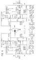
- FIG. 5 A practical high-voltage generator implementation scheme based upon the teachings up to now described is shown in Figure 5.
- an output voltage Vout limiter has been inserted between the voltage multiplier circuit and the load, in order to prevent dangerous and useless over-voltages within the voltage multiplier circuit.
- a feedback loop has been realized around the voltage multiplier circuit, comprising a voltage divider circuit and a voltage controlled oscillator (VCO) by which the clock signal is provided to the input of the voltage multiplier circuit.
- VCO voltage controlled oscillator
- the variation of the output voltage Vout due to a variation of the output current Iout may be minimized by suitably trimming the clock frequency F.
- a voltage multiplier circuit should be made by two or more modules connected in parallel to the output, provided that they use non-overlapping clock signals, in order to reduce the ripple voltage at the output as well as to increase the load current drive capability.
- Vdd 5 volt
- F 10 MHz
- Vout 12 volt
- Iout 1 mA
- N has been set to 2 and therefore ⁇ V is 3 volt.
- Two modules have been used to reduce any ripple effects.
- the capacitance of capacitor C should be (100/3) pF but, taking the transistor capacitance as well as the non-ideal charging and discharging conditions into account, the value of C has been increased by 14% and set to 38.0 pF.
- the resulting designed voltage multiplier circuit is shown in Figure 6.
- SPICE simulation results are shown in Figure 7.
- the output impedance, in a large range around the operation point, is practically constant and less than 2900 Ohms.
- Vdd 5 volt
- F 10 MHz
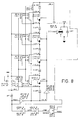
- N has been set to 4 and therefore ⁇ V is 7 volt.
- N 3 is a possible but not recommended value because the tolerance for ⁇ V would be too small. For example, should voltage Vdd drop by 10%, the tolerance ⁇ V would be reduced to zero. Also in this case, two modules have been used in order to reduce the ripple effects.
- the capacitance of capacitor C should be 2.86 pF but, taking the transistor capacitance as well as the non-ideal charging and discharging conditions into account, the value of C has been increased by 26% and set to 3.6 pF. The correction factor is almost proportional to N.
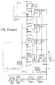
- the resulting designed voltage multiplier circuit is shown in Figure 8. SPICE simulation results are shown in Figure 9. The output impedance, in a large range around the operation point, is practically constant and less than 59 Kohms.
- the largest parasitic capacitance is the one existing between the bottom plate and the underlying layer, which is supposed to be an N-well diffusion whose terminal is electrically isolated.
- the following process data from the 256Kb Flash EEPROM 5 volt only
- plate separation 0.03 ⁇ m
- oxide thickness from the bottom plate to the underlying layer 1 ⁇ m.
- Vout 12 volt
- Iout 1 mA.
- Vout 18 volt
- Iout 100 ⁇ A.
Landscapes
- Engineering & Computer Science (AREA)
- Power Engineering (AREA)
- Dc-Dc Converters (AREA)
- Read Only Memory (AREA)
- Dram (AREA)
- Static Random-Access Memory (AREA)
- Filters That Use Time-Delay Elements (AREA)
Applications Claiming Priority (3)
| Application Number | Priority Date | Filing Date | Title |
|---|---|---|---|
| ITRM940849A IT1275104B (it) | 1994-12-28 | 1994-12-28 | "perfezionato moltiplicatore di tensione on-chip per memorie a semiconduttore" |
| ITRM940849 | 1994-12-28 | ||
| US08/576,281 US5831469A (en) | 1994-12-28 | 1995-12-21 | Multiplier improved voltage |
Publications (3)
| Publication Number | Publication Date |
|---|---|
| EP0720170A2 true EP0720170A2 (fr) | 1996-07-03 |
| EP0720170A3 EP0720170A3 (fr) | 1996-11-27 |
| EP0720170B1 EP0720170B1 (fr) | 2001-04-04 |
Family
ID=26332073
Family Applications (1)
| Application Number | Title | Priority Date | Filing Date |
|---|---|---|---|
| EP95830522A Expired - Lifetime EP0720170B1 (fr) | 1994-12-28 | 1995-12-18 | Multiplicateur de tension amélioré et incorporé sur la puce pour mémoires à semi-conducteurs |
Country Status (4)
| Country | Link |
|---|---|
| US (1) | US5831469A (fr) |
| EP (1) | EP0720170B1 (fr) |
| JP (1) | JPH08287687A (fr) |
| IT (1) | IT1275104B (fr) |
Cited By (5)
| Publication number | Priority date | Publication date | Assignee | Title |
|---|---|---|---|---|
| FR2758021A1 (fr) * | 1996-12-31 | 1998-07-03 | Sgs Thomson Microelectronics | Circuit elevateur de tension |
| EP0851562A3 (fr) * | 1996-12-23 | 1999-06-30 | Texas Instruments Incorporated | Pompe de charge haute tension en particulier pour mémoires EEPROM flash |
| EP0865149A3 (fr) * | 1996-12-23 | 1999-06-30 | Texas Instruments Incorporated | Pompe de charge CMOS à fort courant, en particulier pour mémoires EEPROM flash |
| EP0851561A3 (fr) * | 1996-12-23 | 1999-06-30 | Texas Instruments Incorporated | Pompe de charge à tension de sortie négative, en particulier pour mémoire EEPROM flash |
| US7382634B2 (en) | 2002-10-25 | 2008-06-03 | Nokia Corporation | Voltage multiplier with charge recovery |
Families Citing this family (9)
| Publication number | Priority date | Publication date | Assignee | Title |
|---|---|---|---|---|
| US6072355A (en) * | 1998-01-22 | 2000-06-06 | Burr-Brown Corporation | Bootstrapped CMOS sample and hold circuitry and method |
| US6388392B1 (en) * | 1999-03-23 | 2002-05-14 | Hubbell Incorporated | System for providing auxiliary power to lighting unit for heavy equipment having a direct current power supply and no uninterruptible power supply |
| US6385065B1 (en) * | 2000-09-14 | 2002-05-07 | Fairchild Semiconductor Corporation | Low voltage charge pump employing distributed charge boosting |
| DE10050496B4 (de) * | 2000-10-11 | 2015-04-02 | Texas Instruments Deutschland Gmbh | Gleichspannungswandler |
| US6566847B1 (en) * | 2002-07-29 | 2003-05-20 | Taiwan Semiconductor Manufacturing Company | Low power charge pump regulating circuit |
| JP2008125269A (ja) * | 2006-11-14 | 2008-05-29 | Mcm Japan Kk | 昇圧回路及び降圧回路 |
| TWI496398B (zh) * | 2013-12-31 | 2015-08-11 | Egalax Empia Technology Inc | Use the wiring to change the output voltage of the charge pump |
| US9479050B1 (en) * | 2015-06-26 | 2016-10-25 | Sandisk Technologies Llc | High-efficiency fractional pump |
| WO2018023695A1 (fr) | 2016-08-05 | 2018-02-08 | The University Of Hong Kong | Alimentations électriques à capacité commutée à haut rendement et procédés |
Family Cites Families (9)
| Publication number | Priority date | Publication date | Assignee | Title |
|---|---|---|---|---|
| US4807104A (en) * | 1988-04-15 | 1989-02-21 | Motorola, Inc. | Voltage multiplying and inverting charge pump |
| CH679901A5 (fr) * | 1989-06-20 | 1992-04-30 | Ernst Feller | |
| GB2245112A (en) * | 1990-06-13 | 1991-12-18 | Philips Electronic Associated | Dc/dc voltage multiplier. |
| US5051881A (en) * | 1990-07-05 | 1991-09-24 | Motorola, Inc. | Voltage multiplier |
| US5132895A (en) * | 1990-12-11 | 1992-07-21 | Motorola, Inc. | Variable charge pumping DC-to-DC converter |
| US5111375A (en) * | 1990-12-20 | 1992-05-05 | Texas Instruments Incorporated | Charge pump |
| JPH05244766A (ja) * | 1992-02-27 | 1993-09-21 | Texas Instr Japan Ltd | チャージポンプ回路 |
| US5581454A (en) * | 1994-11-22 | 1996-12-03 | Collins; Hansel | High power switched capacitor voltage conversion and regulation apparatus |
| US5481447A (en) * | 1995-04-27 | 1996-01-02 | Fluke Corporation | Switched capacitance voltage multiplier with commutation |
-
1994
- 1994-12-28 IT ITRM940849A patent/IT1275104B/it active IP Right Grant
-
1995
- 1995-12-18 EP EP95830522A patent/EP0720170B1/fr not_active Expired - Lifetime
- 1995-12-21 US US08/576,281 patent/US5831469A/en not_active Expired - Lifetime
- 1995-12-27 JP JP34154595A patent/JPH08287687A/ja active Pending
Cited By (5)
| Publication number | Priority date | Publication date | Assignee | Title |
|---|---|---|---|---|
| EP0851562A3 (fr) * | 1996-12-23 | 1999-06-30 | Texas Instruments Incorporated | Pompe de charge haute tension en particulier pour mémoires EEPROM flash |
| EP0865149A3 (fr) * | 1996-12-23 | 1999-06-30 | Texas Instruments Incorporated | Pompe de charge CMOS à fort courant, en particulier pour mémoires EEPROM flash |
| EP0851561A3 (fr) * | 1996-12-23 | 1999-06-30 | Texas Instruments Incorporated | Pompe de charge à tension de sortie négative, en particulier pour mémoire EEPROM flash |
| FR2758021A1 (fr) * | 1996-12-31 | 1998-07-03 | Sgs Thomson Microelectronics | Circuit elevateur de tension |
| US7382634B2 (en) | 2002-10-25 | 2008-06-03 | Nokia Corporation | Voltage multiplier with charge recovery |
Also Published As
| Publication number | Publication date |
|---|---|
| JPH08287687A (ja) | 1996-11-01 |
| IT1275104B (it) | 1997-07-30 |
| EP0720170A3 (fr) | 1996-11-27 |
| ITRM940849A0 (it) | 1994-12-28 |
| US5831469A (en) | 1998-11-03 |
| ITRM940849A1 (it) | 1996-06-28 |
| EP0720170B1 (fr) | 2001-04-04 |
Similar Documents
| Publication | Publication Date | Title |
|---|---|---|
| US6359501B2 (en) | Charge-pumping circuits for a low-supply voltage | |
| EP1899785B1 (fr) | Pompe de maintien de charge efficace destinee a une gamme etendue de tensions d'alimentation | |
| US5892267A (en) | Multi-stage voltage-boosting circuit with boosted back-gate bias | |
| US6501325B1 (en) | Low voltage supply higher efficiency cross-coupled high voltage charge pumps | |
| US5905402A (en) | Voltage pump circuit having an independent well-bias voltage | |
| US6130572A (en) | NMOS negative charge pump | |
| US7920018B2 (en) | Booster circuit | |
| US6912159B2 (en) | Boosting circuit and non-volatile semiconductor storage device containing the same | |
| US7046076B2 (en) | High efficiency, low cost, charge pump circuit | |
| EP0720170B1 (fr) | Multiplicateur de tension amélioré et incorporé sur la puce pour mémoires à semi-conducteurs | |
| US5790393A (en) | Voltage multiplier with adjustable output level | |
| US6828849B2 (en) | Voltage generating/transferring circuit | |
| US5347171A (en) | Efficient negative charge pump | |
| US7586361B2 (en) | Semiconductor device comprising a charge pump operated by clock signals | |
| EP0851561B1 (fr) | Pompe de charge à tension de sortie négative, en particulier pour mémoire EEPROM flash | |
| JPH02285959A (ja) | 電圧逓倍回路 | |
| JPH01164264A (ja) | 電圧増倍器集積回路と整流器素子 | |
| US5412257A (en) | High efficiency N-channel charge pump having a primary pump and a non-cascaded secondary pump | |
| KR0167692B1 (ko) | 반도체 메모리장치의 차아지 펌프회로 | |
| US7002399B2 (en) | Basic stage for a charge pump circuit | |
| US7148740B2 (en) | Boost circuit and semiconductor integrated circuit | |
| US7683699B2 (en) | Charge pump | |
| US7808303B2 (en) | Booster circuit | |
| CN101227143A (zh) | 升压电路 | |
| US5926059A (en) | Stacked Charge pump circuit |
Legal Events
| Date | Code | Title | Description |
|---|---|---|---|
| PUAI | Public reference made under article 153(3) epc to a published international application that has entered the european phase |
Free format text: ORIGINAL CODE: 0009012 |
|
| AK | Designated contracting states |
Kind code of ref document: A2 Designated state(s): DE FR GB IT NL |
|
| PUAL | Search report despatched |
Free format text: ORIGINAL CODE: 0009013 |
|
| AK | Designated contracting states |
Kind code of ref document: A3 Designated state(s): DE FR GB IT NL |
|
| 17P | Request for examination filed |
Effective date: 19970505 |
|
| 17Q | First examination report despatched |
Effective date: 19990723 |
|
| GRAG | Despatch of communication of intention to grant |
Free format text: ORIGINAL CODE: EPIDOS AGRA |
|
| GRAG | Despatch of communication of intention to grant |
Free format text: ORIGINAL CODE: EPIDOS AGRA |
|
| GRAH | Despatch of communication of intention to grant a patent |
Free format text: ORIGINAL CODE: EPIDOS IGRA |
|
| GRAH | Despatch of communication of intention to grant a patent |
Free format text: ORIGINAL CODE: EPIDOS IGRA |
|
| GRAA | (expected) grant |
Free format text: ORIGINAL CODE: 0009210 |
|
| AK | Designated contracting states |
Kind code of ref document: B1 Designated state(s): DE FR GB IT NL |
|
| ITF | It: translation for a ep patent filed | ||
| REF | Corresponds to: |
Ref document number: 69520557 Country of ref document: DE Date of ref document: 20010510 |
|
| ET | Fr: translation filed | ||
| REG | Reference to a national code |
Ref country code: GB Ref legal event code: IF02 |
|
| PLBE | No opposition filed within time limit |
Free format text: ORIGINAL CODE: 0009261 |
|
| STAA | Information on the status of an ep patent application or granted ep patent |
Free format text: STATUS: NO OPPOSITION FILED WITHIN TIME LIMIT |
|
| 26N | No opposition filed | ||
| PGFP | Annual fee paid to national office [announced via postgrant information from national office to epo] |
Ref country code: IT Payment date: 20061231 Year of fee payment: 12 |
|
| PG25 | Lapsed in a contracting state [announced via postgrant information from national office to epo] |
Ref country code: IT Free format text: LAPSE BECAUSE OF NON-PAYMENT OF DUE FEES Effective date: 20071218 |
|
| PGFP | Annual fee paid to national office [announced via postgrant information from national office to epo] |
Ref country code: NL Payment date: 20101124 Year of fee payment: 16 Ref country code: FR Payment date: 20101203 Year of fee payment: 16 |
|
| PGFP | Annual fee paid to national office [announced via postgrant information from national office to epo] |
Ref country code: GB Payment date: 20101123 Year of fee payment: 16 |
|
| PGFP | Annual fee paid to national office [announced via postgrant information from national office to epo] |
Ref country code: DE Payment date: 20101230 Year of fee payment: 16 |
|
| REG | Reference to a national code |
Ref country code: NL Ref legal event code: V1 Effective date: 20120701 |
|
| GBPC | Gb: european patent ceased through non-payment of renewal fee |
Effective date: 20111218 |
|
| REG | Reference to a national code |
Ref country code: FR Ref legal event code: ST Effective date: 20120831 |
|
| REG | Reference to a national code |
Ref country code: DE Ref legal event code: R119 Ref document number: 69520557 Country of ref document: DE Effective date: 20120703 |
|
| PG25 | Lapsed in a contracting state [announced via postgrant information from national office to epo] |
Ref country code: DE Free format text: LAPSE BECAUSE OF NON-PAYMENT OF DUE FEES Effective date: 20120703 Ref country code: GB Free format text: LAPSE BECAUSE OF NON-PAYMENT OF DUE FEES Effective date: 20111218 |
|
| PG25 | Lapsed in a contracting state [announced via postgrant information from national office to epo] |
Ref country code: NL Free format text: LAPSE BECAUSE OF NON-PAYMENT OF DUE FEES Effective date: 20120701 |
|
| PG25 | Lapsed in a contracting state [announced via postgrant information from national office to epo] |
Ref country code: FR Free format text: LAPSE BECAUSE OF NON-PAYMENT OF DUE FEES Effective date: 20120102 |