EP0720217A2 - Elektrostatischer Halter und sein Wirkungsverfahren - Google Patents
Elektrostatischer Halter und sein WirkungsverfahrenInfo
- Publication number
- EP0720217A2 EP0720217A2 EP95120282A EP95120282A EP0720217A2 EP 0720217 A2 EP0720217 A2 EP 0720217A2 EP 95120282 A EP95120282 A EP 95120282A EP 95120282 A EP95120282 A EP 95120282A EP 0720217 A2 EP0720217 A2 EP 0720217A2
- Authority
- EP
- European Patent Office
- Prior art keywords
- ejector pins
- ejector
- wafer
- rear surface
- electrostatic chuck
- Prior art date
- Legal status (The legal status is an assumption and is not a legal conclusion. Google has not performed a legal analysis and makes no representation as to the accuracy of the status listed.)
- Granted
Links
Images


Classifications
-
- H—ELECTRICITY
- H10—SEMICONDUCTOR DEVICES; ELECTRIC SOLID-STATE DEVICES NOT OTHERWISE PROVIDED FOR
- H10P—GENERIC PROCESSES OR APPARATUS FOR THE MANUFACTURE OR TREATMENT OF DEVICES COVERED BY CLASS H10
- H10P72/00—Handling or holding of wafers, substrates or devices during manufacture or treatment thereof
- H10P72/70—Handling or holding of wafers, substrates or devices during manufacture or treatment thereof for supporting or gripping
- H10P72/72—Handling or holding of wafers, substrates or devices during manufacture or treatment thereof for supporting or gripping using electrostatic chucks
- H10P72/722—Details of electrostatic chucks
-
- H—ELECTRICITY
- H10—SEMICONDUCTOR DEVICES; ELECTRIC SOLID-STATE DEVICES NOT OTHERWISE PROVIDED FOR
- H10P—GENERIC PROCESSES OR APPARATUS FOR THE MANUFACTURE OR TREATMENT OF DEVICES COVERED BY CLASS H10
- H10P72/00—Handling or holding of wafers, substrates or devices during manufacture or treatment thereof
- H10P72/70—Handling or holding of wafers, substrates or devices during manufacture or treatment thereof for supporting or gripping
- H10P72/76—Handling or holding of wafers, substrates or devices during manufacture or treatment thereof for supporting or gripping using mechanical means, e.g. clamps or pinches
- H10P72/7604—Handling or holding of wafers, substrates or devices during manufacture or treatment thereof for supporting or gripping using mechanical means, e.g. clamps or pinches the wafers being placed on a susceptor, stage or support
- H10P72/7612—Handling or holding of wafers, substrates or devices during manufacture or treatment thereof for supporting or gripping using mechanical means, e.g. clamps or pinches the wafers being placed on a susceptor, stage or support characterised by lifting arrangements, e.g. lift pins
-
- Y—GENERAL TAGGING OF NEW TECHNOLOGICAL DEVELOPMENTS; GENERAL TAGGING OF CROSS-SECTIONAL TECHNOLOGIES SPANNING OVER SEVERAL SECTIONS OF THE IPC; TECHNICAL SUBJECTS COVERED BY FORMER USPC CROSS-REFERENCE ART COLLECTIONS [XRACs] AND DIGESTS
- Y10—TECHNICAL SUBJECTS COVERED BY FORMER USPC
- Y10T—TECHNICAL SUBJECTS COVERED BY FORMER US CLASSIFICATION
- Y10T279/00—Chucks or sockets
- Y10T279/23—Chucks or sockets with magnetic or electrostatic means
Definitions
- the present invention relates to an electrostatic chuck used to clamp a workpiece such as a semiconductor wafer, and particularly to an electrostatic chuck used for the sample stage of a plasma processing apparatus.
- Electrostatic chucks are used for sample stages of etching apparatus and CVD apparatus for clamping workpieces such as semiconductor wafers.
- the so-called monopolar chuck is made up of an electrode, a dielectric film which covers the clamping surface of a workpiece so as to insulate the workpiece from the electrode, and means of applying a DC voltage between the workpiece and the electrode.
- the electrostatic chuck of this type operates to apply a DC voltage between the electrode and workpiece interposed by the dielectric film so as to generate a static charge, thereby clamping the workpiece based on the Coulomb force exerting between these members.
- Japanese Patent Application Laid-open No. 4-253356 describes a method of eliminating a accumulated charge from the wafer by grounding it when it is released.
- Japanese Patent Application Laid-open No.5-226292 describes a method of supplying a charge to the wafer by grounding it when it is clamped and eliminating a accumulated charge from the wafer by grounding it when it is released.
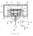
- Fig.1 is a longitudinal cross-sectional diagram of a plasma processing apparatus equipped with an electrostatic chuck which supplies a charge to and eliminates a accumulated charge from the workpiece through ejector pins.
- the electrostatic chuck 11 includes an electrode 12 of aluminum (Al) or the like which is coated with a dielectric film 13 of alumina (Al 2 O 3 ), and it is disposed on a base 14.
- the electrode 12 is connected to a DC power source 27, which applies a DC voltage to the electrode 12, by way of a switch 26.
- a filter (not shown) for protecting the DC power source 27 is connected between the switch 26 and the DC power source 27.
- the electrode 12 has in it a liquid circulation path (not shown), and the temperature of the wafer 1 can be controlled by the conduction of heat.
- the electrostatic chuck 11 and the base 14 have four apertures (only two apertures are shown in Fig.1) penetrating from the upper surface of the electrostatic chuck 11 to the bottom surface of the base 14 so that ejector pins 16 can run through.
- the four ejector pins 16 are coupled by means of an ejector pin coupling plate 17 to a drive shaft 21 which runs through a aperture in the bottom plate 15 of the frame.
- the drive shaft 21 is connected to an air cylinder 23, and the ejector pins 16 are moved up and down by the operation of the air cylinder 23.
- a slide guide 24 is provided around the drive shaft 21 in the aperture of the bottom plate 15, a bellows 25 is provided to surround the part of the drive shaft 21 between the bottom plate 15 and a seal plate 22, and a reaction chamber 51 is sealed airtightly.
- the ejector pins 16, coupling plate 17 and drive shaft 21 are made of metal such as stainless steel (JIS-SUS316) or the like, and the ejector pins 16 can be grounded by way of the coupling plate 17, drive shaft 21 and a switch 30.
- the electrode 12 which also works as a lower electrode is connected to a high-frequency (RF) power source 29 by way of a switch 28.
- a capacitor (not shown) for blocking a DC current and an impedance matching device (not shown) are connected between the switch 28 and the RF power source 29.
- the electrostatic chuck 11 has its peripheral section protected by a shielding member 46 of alumina or the like.
- the reaction chamber 51 Disposed over the electrostatic chuck 11 is an upper electrode 41, and its peripheral section is protected by a shielding member 42.
- the upper electrode 41 is grounded.
- the upper electrode 41 is made of aluminum or the like, and the shielding member 42 is made of insulator such as alumina.
- the reaction chamber 51 has its wall 43 made of metal such as aluminum, and it is grounded. Processing gas is introduced into the reaction chamber 51 through a gas inlet 44, and the gas is evacuated by an evacuation pump (not shown) through a gas outlet 45.
- the wafer 1 is moved to the position over the electrostatic chuck 11 by means of a transfer arm (not shown).
- the ejector pins 16, which are grounded in advance by turning on the switch 30, are moved up to lift the wafer 1, and thereafter the transfer arm retreats.
- the switch 26 is turned on to apply the DC voltage to the electrode 12, and the ejector pins 16 are moved down, thereby placing the wafer 1 on the electrostatic chuck 11. A charge is supplied to the wafer 1 through the ejector pins 16, and it is clamped to the electrostatic chuck 11 by the Coulomb force.
- Processing gas is introduced into the reaction chamber 51.
- the ejector pins 16 are further moved down to make a sufficient clearance from the rear surface of the wafer 1, and the switch 30 is turned off so that the ejector pins 16 are disconnected from the ground.
- the switch 28 is turned on to apply the RF power from the RF power source 29 to the lower electrode 12. Consequently, plasma is generated in the reaction chamber 51, and the wafer 1 is processed by the plasma. After finishing the intended plasma processing, RF power application is stopped.
- the switch 26 is turned off to stop the DC voltage application to the electrode 12, and the switch 30 is turned on to ground the wafer 1 through the ejector pins 16.
- the accumulated charge of the wafer 1 is eliminated and the clamping force between the wafer 1 and the electrostatic chuck 11 diminishes.
- the ejector pins 16 are moved up to lift the wafer 1 off the electrostatic chuck 11, and it is taken out of the reaction chamber 51 by the transfer arm (not shown).
- the electrostatic chuck arranged as explained above it is necessary for the electrostatic chuck arranged as explained above to have its ejector pins brought to tight contact with the rear surface of the wafer while it is placed on the electrostatic chuck so that a charge is surely supplied to the wafer for clamping and surely eliminated from the wafer for releasing.
- a discharge occurs in the gap between an ejector pin and the wafer rear surface, even in case the pins are disconnected from the ground, during the plasma processing of the wafer.
- This discharge induces problems: (1) The wafer heats up locally; (2) The dielectric film of the electrostatic chuck damages; (3) An insulating substance deposits on the tips of the ejector pins, deteriorating the conductivity of the ejector pins, resulting in extended wafer clamping and releasing times.
- the present invention is intended to overcome the foregoing prior art deficiencies, and its object is to provide an electrostatic chuck capable of bringing the ejector pins to tight contact with the wafer rear surface so that the wafer can be clamped and released quickly.
- Another object of the present invention is to provide methods of operating the electrostatic chuck for preventing the discharge in the gap between an ejector pin and the wafer rear surface during the plasma processing of wafer, thereby dissolving the above-mentioned problems associated with the discharge.
- the electrostatic chuck of this invention includes an ejector buffer mechanism, such as springs, for ejector pins so that the ejector pins are brought to tight contact with the wafer rear surface.
- the ejector buffer mechanism is designed to offset the disparity of clearance of individual ejector pins from the wafer rear surface. Consequently, all ejector pins can be brought to tight contact with the rear surface of the wafer by controlling the position of the ejector pins within a certain range of accuracy.
- the ejector buffer mechanism eliminates the need of a high-precision control mechanism for the ejector drive means, while enabling the quick and reliable clamping and releasing of a wafer.
- this invention provides two methods of operating the electrostatic chuck for the plasma processing of a wafer.
- the first method is to disconnect all ejector pins from the ground and keep the pins in contact with the wafer rear surface so that the wafer and ejector pins have the same potential. Consequently, discharge which would occur in the gap between these members is prevented, and the problems associated with this discharge are dissolved.
- the inventors of the present invention found the fact that when the ejector pins are kept in contact with the wafer rear surface during the plasma processing, in wiring process for example, charge-up damage is occasionally induced in the insulating film on the wafer.
- the presumed cause of this charge-up damage is that the ejector pins work as load resistors and load capacitors to vary the potential distribution on the surface of the wafer, and positive ions in the plasma gather to the contact points of the ejector pins on the wafer, causing positive charges to increase at these positions. It was confirmed that the charge-up damage can be suppressed by separating the ejector pins off the wafer rear surface during the plasma processing.
- the inventors further studied to prevent the discharge in the gap between an ejector pin and the wafer rear surface, while suppressing the charge-up damage by letting the ejector pins be in non-contact with the wafer rear surface, and found that the discharge occurs dependent on the amount of clearance of the ejector pins from wafer rear surface and that the discharge can be suppressed by making the clearance small enough.
- the second method of operation is to disconnect all ejector pins from the ground during the plasma processing of wafer and control the clearance between the ejector pins and wafer rear surface within a certain range of length in which the discharge does not occur. Consequently, the discharge in the gap between an ejector pin and the wafer rear surface can be suppressed and, at the same time, the charge-up damage induced in the insulating film of the wafer during the plasma processing for wiring process or the like can be prevented.
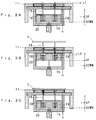
- Fig.2 shows a plasma processing apparatus equipped with the electrostatic chuck based on an embodiment, and the following explains only portions different from the apparatus with the conventional electrostatic chuck shown in Fig.1.
- electrostatic chuck In the conventional electrostatic chuck, the ejector pins 16 are coupled to the drive shaft 21 through the ejector pin coupling plate 17, whereas electrostatic chuck of this embodiment is designed to couple the ejector pins 16 to the drive shaft 21 through an ejector buffer mechanism which is made up of an ejector pin housing 19 and springs 20 seated in it.
- the ejector pin housing 19 consists of a housing base 19b of stainless steel (JIS-SUS316), with bores 19c for seating the springs 20 being formed therein, and a housing top 19a made of polyimide.
- the ejector pins 16 are fixed to individual pin flanges 18, which are connected to the ejector pin housing 19 through the individual springs 20 seated in the bores 19c.
- the spring action of the springs 20 moderates the vertical movement of the individual ejector pins 16 caused by the vertical movement of the drive shaft 21.
- the springs 20 used in this embodiment are coil springs made of stainless steel.
- the ejector pins 16 are grounded by way of the pin flanges 18, springs 20, housing base 19b and drive shaft 21 when the switch 30 is turned on.
- the coil springs used for the ejector buffer mechanism of this embodiment may obviously be replaced with leaf springs or air cushion devices and so on.
- the ejector pins 16 have their vertical position defined in terms of the position of the bottom surface of the ejector pin housing 19 as a reference position.
- the ejector pins 16 take the high position and low position when the reference position is at positions UP and DOWN, respectively.
- the DOWN position is determined as follows. In the absence of a wafer on the ejector pins 16, they are assumed to come out their tips over the upper surface of the electrostatic chuck 11 by a length of L1. When a wafer 1 is placed on the ejector pins 16, the springs 20 are assumed to be compressed by a length of L2. The DOWN position is determined such that L1 is smaller than L2. In this embodiment, L1 and L2 are set to be 0.5 mm and 1.0 mm, respectively.
- the ejector pin drive means can allow 0.5 mm (L1) for its control accuracy based on 1.0 mm (L2) of the compression length of the springs when loaded with a wafer, it was confirmed that the ejector pins can be brought to tight contact with the wafer rear surface.
- the mechanism of this embodiment facilitates the positioning control of the ejector pins, speeds up the clamping and releasing of a wafer, and suppresses the occurrence of discharge in the gap between an ejector pin and the wafer rear surface.
- the ejector pins 16 have another vertical position DOWN2 defined, in addition to the UP and DOWN positions in the preceding embodiment.
- the DOWN2 position is below the DOWN position encountered when the ejector pin housing 19 is further lowered, and it is determined such that discharge does not occur in the gap L3 between an ejector pin 16 and the wafer rear surface in a state of expansion of all springs 20.
- L1, L2 and L3 are set to be 0.5 mm, 1.0 mm and 0.5 mm, respectively.
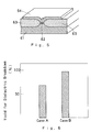
- the charge-up damage were evaluated for the method of operation of keeping the ejector pin tip in tight contact with the wafer rear surface during the plasma processing and the method of operation of allowing a clearance of 0.5 mm for the ejector pin tip from wafer rear surface during the plasma processing.
- An antenna MOS (Metal Oxide Semiconductor) element shown in Fig.5 was used for the evaluation of charge-up damage. It consists of a p-type silicon wafer 61, a gate insulator film 62 of silicon oxide (SiO 2 ), a field oxide film 63 of thermal silicon oxide (SiO 2 ), and a gate electrode of poly-silicon 64.
- the antenna ratio is 64 ⁇ 10 4
- the gate insulator film has a thickness of 8 nm.
- Silicon oxide films (SiO 2 ) were formed on wafers, with the antenna MOS elements being formed, and the silicon oxide films were etched back in the plasma processing apparatus equipped with the electrostatic chuck shown in Fig.2, thereby evaluating the yield of antenna MOS elements that survived the dielectric breakdown.
- the silicon oxide film was formed to have a thickness of 250 nm based on the LPCVD process.
- the conditions of etch-back were as follows. Ar: 400 sccm, CF 4 : 20 sccm, CHF 3 : 30 sccm, pressure: 250 mTorr, frequency of RF voltage: 13.56 MHz, RF power: 800 W, spacing of electrode: 11 mm.
- Fig.6 shows the result of the yield of antenna MOS elements that survived the dielectric breakdown.
- Case A is of the condition of etch-back in which the ejector pin tip is brought to contact with the wafer rear surface
- case B is of the condition of etch-back in which a clearance of 0.5 mm is allowed for the ejector pin tip from the wafer rear surface.
- the graph reveals the improvement by case B of the yield of antenna MOS elements. It was confirmed that the charge-up damage to the insulator film can be reduced by allowing a clearance of 0.5 mm for the ejector pin from the wafer rear surface during the plasma processing.
- a charge is supplied to and eliminated from the wafer through the ejector pins at both clamping and releasing of the wafer, it is obvious that charge supply and elimination operations may be assisted by the exposure of inert gas plasma such as Ar gas plasma.
- the electrostatic chuck of this invention facilitates the positioning control of the ejector pins and enables the ejector pins to come in tight contact with the wafer rear surface, and consequently a wafer can be clamped and released quickly and reliably.
- the ejector pins are brought to tight contact with the wafer rear surface, thereby suppressing the occurrence of discharge in the gap between an ejector pin and the wafer rear surface, and the problems associated with this discharge can be dissolved.
- a clearance within a prescribed range is created for the ejector pins from the wafer rear surface, thereby suppressing the occurrence of discharge in the gap between an ejector pin and the wafer rear surface, and charge-up damage to the wafer can be reduced.
Landscapes
- Container, Conveyance, Adherence, Positioning, Of Wafer (AREA)
- Jigs For Machine Tools (AREA)
- Drying Of Semiconductors (AREA)
Applications Claiming Priority (6)
| Application Number | Priority Date | Filing Date | Title |
|---|---|---|---|
| JP327150/94 | 1994-12-28 | ||
| JP32715094 | 1994-12-28 | ||
| JP32715094 | 1994-12-28 | ||
| JP182836/95 | 1995-07-19 | ||
| JP18283695 | 1995-07-19 | ||
| JP18283695A JP3082624B2 (ja) | 1994-12-28 | 1995-07-19 | 静電チャックの使用方法 |
Publications (3)
| Publication Number | Publication Date |
|---|---|
| EP0720217A2 true EP0720217A2 (de) | 1996-07-03 |
| EP0720217A3 EP0720217A3 (de) | 1996-07-17 |
| EP0720217B1 EP0720217B1 (de) | 2000-08-16 |
Family
ID=26501488
Family Applications (1)
| Application Number | Title | Priority Date | Filing Date |
|---|---|---|---|
| EP95120282A Expired - Lifetime EP0720217B1 (de) | 1994-12-28 | 1995-12-21 | Elektrostatischer Halter |
Country Status (5)
| Country | Link |
|---|---|
| US (1) | US5815366A (de) |
| EP (1) | EP0720217B1 (de) |
| JP (1) | JP3082624B2 (de) |
| KR (1) | KR100286622B1 (de) |
| DE (1) | DE69518398D1 (de) |
Cited By (5)
| Publication number | Priority date | Publication date | Assignee | Title |
|---|---|---|---|---|
| EP1391786A1 (de) * | 2002-08-23 | 2004-02-25 | ASML Netherlands B.V. | Halter, lithographisches Gerät und Verfahren zur Herstellung einer Vorrichtung |
| US7092231B2 (en) | 2002-08-23 | 2006-08-15 | Asml Netherlands B.V. | Chuck, lithographic apparatus and device manufacturing method |
| US7952851B2 (en) | 2008-10-31 | 2011-05-31 | Axcelis Technologies, Inc. | Wafer grounding method for electrostatic clamps |
| US8902560B2 (en) * | 2008-10-31 | 2014-12-02 | Axcelis Technologies, Inc. | Electrostatic chuck ground punch |
| CN112518364A (zh) * | 2020-10-27 | 2021-03-19 | 合肥哈工联进智能装备有限公司 | 一种用于工装锁紧的脱能式设备 |
Families Citing this family (43)
| Publication number | Priority date | Publication date | Assignee | Title |
|---|---|---|---|---|
| JP3249765B2 (ja) * | 1997-05-07 | 2002-01-21 | 東京エレクトロン株式会社 | 基板処理装置 |
| JP3163973B2 (ja) * | 1996-03-26 | 2001-05-08 | 日本電気株式会社 | 半導体ウエハ・チャック装置及び半導体ウエハの剥離方法 |
| JP3954177B2 (ja) * | 1997-01-29 | 2007-08-08 | 日本碍子株式会社 | 金属部材とセラミックス部材との接合構造およびその製造方法 |
| US6456480B1 (en) * | 1997-03-25 | 2002-09-24 | Tokyo Electron Limited | Processing apparatus and a processing method |
| AT411304B (de) * | 1997-06-18 | 2003-11-25 | Sez Ag | Träger für scheibenförmige gegenstände, insbesondere silizium-wafer |
| US6033482A (en) * | 1998-04-10 | 2000-03-07 | Applied Materials, Inc. | Method for igniting a plasma in a plasma processing chamber |
| JP3298528B2 (ja) * | 1998-12-10 | 2002-07-02 | 日本電気株式会社 | 回路設計方法および装置、情報記憶媒体、集積回路装置 |
| US6169652B1 (en) * | 1999-03-12 | 2001-01-02 | Euv, L.L.C. | Electrostatically screened, voltage-controlled electrostatic chuck |
| JP2001057359A (ja) * | 1999-08-17 | 2001-02-27 | Tokyo Electron Ltd | プラズマ処理装置 |
| EP1217655A1 (de) * | 2000-12-23 | 2002-06-26 | VenTec Gesellschaft für Venturekapital und Unternehmensberatung | Methode zur Handhabung dünner Wafer |
| US20020126437A1 (en) * | 2001-03-12 | 2002-09-12 | Winbond Electronics Corporation | Electrostatic chuck system and method for maintaining the same |
| US6481723B1 (en) * | 2001-03-30 | 2002-11-19 | Lam Research Corporation | Lift pin impact management |
| US6665168B2 (en) * | 2001-03-30 | 2003-12-16 | Taiwan Semiconductor Manufacturing Co. Ltd | Electrostatic chuck apparatus and method for efficiently dechucking a substrate therefrom |
| TWI246873B (en) | 2001-07-10 | 2006-01-01 | Tokyo Electron Ltd | Plasma processing device |
| US6864563B1 (en) * | 2002-05-30 | 2005-03-08 | Lsi Logic Corporation | Grounding mechanism for semiconductor devices |
| JP2004152929A (ja) * | 2002-10-30 | 2004-05-27 | Nec Electronics Corp | 半導体装置及びその製造方法 |
| US7500445B2 (en) * | 2003-01-27 | 2009-03-10 | Applied Materials, Inc. | Method and apparatus for cleaning a CVD chamber |
| US7301623B1 (en) * | 2003-12-16 | 2007-11-27 | Nanometrics Incorporated | Transferring, buffering and measuring a substrate in a metrology system |
| US20060162739A1 (en) * | 2005-01-21 | 2006-07-27 | Nikon Corporation | Cleaning chuck in situ |
| CN100343952C (zh) * | 2005-12-05 | 2007-10-17 | 北京北方微电子基地设备工艺研究中心有限责任公司 | 一种硅片卸载工艺 |
| CN100362645C (zh) * | 2005-12-07 | 2008-01-16 | 北京北方微电子基地设备工艺研究中心有限责任公司 | 顶针装置 |
| CN101352108B (zh) * | 2005-12-28 | 2011-12-07 | 夏普株式会社 | 台装置和等离子体处理装置 |
| US20070212200A1 (en) * | 2006-03-09 | 2007-09-13 | Tokyo Electron Limited | Lifter and target object processing apparatus provided with lifter |
| JP4933814B2 (ja) * | 2006-03-30 | 2012-05-16 | 株式会社ブイ・テクノロジー | 作業装置におけるワーク受け渡し装置 |
| JP2008198739A (ja) | 2007-02-09 | 2008-08-28 | Tokyo Electron Ltd | 載置台構造、これを用いた処理装置及びこの装置の使用方法 |
| US8497980B2 (en) * | 2007-03-19 | 2013-07-30 | Nikon Corporation | Holding apparatus, exposure apparatus, exposure method, and device manufacturing method |
| JP5302541B2 (ja) * | 2008-01-09 | 2013-10-02 | 株式会社日立ハイテクノロジーズ | プラズマ処理装置 |
| US9953849B2 (en) | 2008-06-20 | 2018-04-24 | Varian Semiconductor Equipment Associates, Inc. | Platen for reducing particle contamination on a substrate and a method thereof |
| US8681472B2 (en) * | 2008-06-20 | 2014-03-25 | Varian Semiconductor Equipment Associates, Inc. | Platen ground pin for connecting substrate to ground |
| JP2010087342A (ja) * | 2008-10-01 | 2010-04-15 | Toray Eng Co Ltd | リフトピン |
| JP2010087343A (ja) * | 2008-10-01 | 2010-04-15 | Toray Eng Co Ltd | 基板処理装置及び基板載置方法 |
| US11978611B2 (en) * | 2009-05-01 | 2024-05-07 | Advanced Energy Industries, Inc. | Apparatus with switches to produce a waveform |
| US11615941B2 (en) | 2009-05-01 | 2023-03-28 | Advanced Energy Industries, Inc. | System, method, and apparatus for controlling ion energy distribution in plasma processing systems |
| DE102011011531B4 (de) * | 2011-02-17 | 2014-08-14 | Audi Ag | Auswerferanordnung zur Entformung eines Gussbauteils aus einer Gießform eines Gießwerkzeugs |
| WO2013049586A1 (en) * | 2011-09-30 | 2013-04-04 | Applied Materials, Inc. | Electrostatic chuck |
| US9999947B2 (en) * | 2015-05-01 | 2018-06-19 | Component Re-Engineering Company, Inc. | Method for repairing heaters and chucks used in semiconductor processing |
| KR102615853B1 (ko) * | 2015-10-15 | 2023-12-21 | 어플라이드 머티어리얼스, 인코포레이티드 | 기판 캐리어 시스템 |
| US10438833B2 (en) * | 2016-02-16 | 2019-10-08 | Lam Research Corporation | Wafer lift ring system for wafer transfer |
| JP7170449B2 (ja) * | 2018-07-30 | 2022-11-14 | 東京エレクトロン株式会社 | 載置台機構、処理装置及び載置台機構の動作方法 |
| CN109985823A (zh) * | 2019-05-06 | 2019-07-09 | 山东泓瑞光电科技有限公司 | 一种led晶片自动分选机用缓冲过渡平台 |
| US12181801B2 (en) | 2021-05-03 | 2024-12-31 | Applied Materials, Inc. | Chamber and methods of treating a substrate after exposure to radiation |
| US12567572B2 (en) | 2023-07-11 | 2026-03-03 | Advanced Energy Industries, Inc. | Plasma behaviors predicted by current measurements during asymmetric bias waveform application |
| WO2026006812A1 (en) * | 2024-06-27 | 2026-01-02 | Axcelis Technologies, Inc. | Direct voltage control of a clamping surface of an electrostatic clamp |
Family Cites Families (12)
| Publication number | Priority date | Publication date | Assignee | Title |
|---|---|---|---|---|
| JPS60121970A (ja) * | 1983-12-01 | 1985-06-29 | Toshiba Mach Co Ltd | 静電チャック |
| JPS63131521A (ja) * | 1986-11-21 | 1988-06-03 | Tokuda Seisakusho Ltd | ドライエツチング装置 |
| JP2692323B2 (ja) * | 1989-08-08 | 1997-12-17 | 富士電機株式会社 | 半導体ウエハ保持装置 |
| US5179498A (en) * | 1990-05-17 | 1993-01-12 | Tokyo Electron Limited | Electrostatic chuck device |
| JP3230821B2 (ja) * | 1991-01-28 | 2001-11-19 | 株式会社東芝 | プッシャーピン付き静電チャック |
| JPH05129421A (ja) * | 1991-11-07 | 1993-05-25 | Fujitsu Ltd | 静電チヤツク |
| US5310453A (en) * | 1992-02-13 | 1994-05-10 | Tokyo Electron Yamanashi Limited | Plasma process method using an electrostatic chuck |
| JPH05226292A (ja) * | 1992-02-13 | 1993-09-03 | Tokyo Electron Yamanashi Kk | プラズマ処理開始方法 |
| US5382311A (en) * | 1992-12-17 | 1995-01-17 | Tokyo Electron Limited | Stage having electrostatic chuck and plasma processing apparatus using same |
| JP3264391B2 (ja) * | 1993-05-17 | 2002-03-11 | 東京エレクトロン株式会社 | 静電吸着体の離脱装置 |
| JPH06252253A (ja) * | 1993-02-26 | 1994-09-09 | Sumitomo Metal Ind Ltd | 静電チャック |
| US5459632A (en) * | 1994-03-07 | 1995-10-17 | Applied Materials, Inc. | Releasing a workpiece from an electrostatic chuck |
-
1995
- 1995-07-19 JP JP18283695A patent/JP3082624B2/ja not_active Expired - Fee Related
- 1995-12-20 US US08/575,864 patent/US5815366A/en not_active Expired - Fee Related
- 1995-12-21 DE DE69518398T patent/DE69518398D1/de not_active Expired - Lifetime
- 1995-12-21 EP EP95120282A patent/EP0720217B1/de not_active Expired - Lifetime
- 1995-12-27 KR KR1019950058350A patent/KR100286622B1/ko not_active Expired - Fee Related
Cited By (5)
| Publication number | Priority date | Publication date | Assignee | Title |
|---|---|---|---|---|
| EP1391786A1 (de) * | 2002-08-23 | 2004-02-25 | ASML Netherlands B.V. | Halter, lithographisches Gerät und Verfahren zur Herstellung einer Vorrichtung |
| US7092231B2 (en) | 2002-08-23 | 2006-08-15 | Asml Netherlands B.V. | Chuck, lithographic apparatus and device manufacturing method |
| US7952851B2 (en) | 2008-10-31 | 2011-05-31 | Axcelis Technologies, Inc. | Wafer grounding method for electrostatic clamps |
| US8902560B2 (en) * | 2008-10-31 | 2014-12-02 | Axcelis Technologies, Inc. | Electrostatic chuck ground punch |
| CN112518364A (zh) * | 2020-10-27 | 2021-03-19 | 合肥哈工联进智能装备有限公司 | 一种用于工装锁紧的脱能式设备 |
Also Published As
| Publication number | Publication date |
|---|---|
| JPH08236604A (ja) | 1996-09-13 |
| EP0720217A3 (de) | 1996-07-17 |
| KR960026538A (ko) | 1996-07-22 |
| JP3082624B2 (ja) | 2000-08-28 |
| DE69518398D1 (de) | 2000-09-21 |
| EP0720217B1 (de) | 2000-08-16 |
| KR100286622B1 (ko) | 2001-05-02 |
| US5815366A (en) | 1998-09-29 |
Similar Documents
| Publication | Publication Date | Title |
|---|---|---|
| US5815366A (en) | Electrostatic chuck and the method of operating the same | |
| US7126808B2 (en) | Wafer platen equipped with electrostatic clamp, wafer backside gas cooling, and high voltage operation capability for plasma doping | |
| US5460684A (en) | Stage having electrostatic chuck and plasma processing apparatus using same | |
| US6243251B1 (en) | Electrostatic chuck, and method of and apparatus for processing sample using the chuck | |
| US7258811B2 (en) | Wafer stage including electrostatic chuck and method for dechucking wafer using the wafer stage | |
| JP2879887B2 (ja) | プラズマ処理方法 | |
| US6174370B1 (en) | Semiconductor wafer chucking device and method for stripping semiconductor wafer | |
| KR102919552B1 (ko) | 플라즈마 처리 장치, 및 피처리체의 반송 방법 | |
| JP2001093884A (ja) | プラズマ処理装置およびプラズマ処理方法 | |
| JP4322484B2 (ja) | プラズマ処理方法及びプラズマ処理装置 | |
| JP3182615B2 (ja) | プラズマ処理方法および装置 | |
| JPH08335568A (ja) | エッチング装置 | |
| US20030236004A1 (en) | Dechucking with N2/O2 plasma | |
| KR0171062B1 (ko) | 드라이에칭장치 | |
| JPH1027780A (ja) | プラズマ処理方法 | |
| JP3269678B2 (ja) | 静電チャック装置および静電チャック方法 | |
| US12521773B2 (en) | Method of cleaning electrostatic chuck and method of manufacturing semiconductor device while exposing electrostatic chuck to plasma and introducing electron current | |
| JPH08293486A (ja) | 真空処理方法及び装置 | |
| JP3027781B2 (ja) | プラズマ処理方法 | |
| JPH0737862A (ja) | 低温処理装置 | |
| JP3131865B2 (ja) | プラズマ成膜装置 | |
| JP2004087576A (ja) | 真空処理装置 | |
| JPH07176586A (ja) | プラズマ処理装置 | |
| JP3485335B2 (ja) | プラズマ処理装置の静電チャック | |
| KR0166851B1 (ko) | 웨이퍼의 언로딩 방법 |
Legal Events
| Date | Code | Title | Description |
|---|---|---|---|
| PUAI | Public reference made under article 153(3) epc to a published international application that has entered the european phase |
Free format text: ORIGINAL CODE: 0009012 |
|
| PUAL | Search report despatched |
Free format text: ORIGINAL CODE: 0009013 |
|
| AK | Designated contracting states |
Kind code of ref document: A2 Designated state(s): DE FR GB NL |
|
| AK | Designated contracting states |
Kind code of ref document: A3 Designated state(s): DE FR GB NL |
|
| 17P | Request for examination filed |
Effective date: 19970109 |
|
| 17Q | First examination report despatched |
Effective date: 19970605 |
|
| RTI1 | Title (correction) |
Free format text: ELECTROSTATIC CHUCK |
|
| GRAG | Despatch of communication of intention to grant |
Free format text: ORIGINAL CODE: EPIDOS AGRA |
|
| GRAG | Despatch of communication of intention to grant |
Free format text: ORIGINAL CODE: EPIDOS AGRA |
|
| GRAH | Despatch of communication of intention to grant a patent |
Free format text: ORIGINAL CODE: EPIDOS IGRA |
|
| GRAH | Despatch of communication of intention to grant a patent |
Free format text: ORIGINAL CODE: EPIDOS IGRA |
|
| GRAA | (expected) grant |
Free format text: ORIGINAL CODE: 0009210 |
|
| AK | Designated contracting states |
Kind code of ref document: B1 Designated state(s): DE FR GB NL |
|
| PG25 | Lapsed in a contracting state [announced via postgrant information from national office to epo] |
Ref country code: NL Free format text: LAPSE BECAUSE OF FAILURE TO SUBMIT A TRANSLATION OF THE DESCRIPTION OR TO PAY THE FEE WITHIN THE PRESCRIBED TIME-LIMIT Effective date: 20000816 |
|
| ET | Fr: translation filed | ||
| REF | Corresponds to: |
Ref document number: 69518398 Country of ref document: DE Date of ref document: 20000921 |
|
| PG25 | Lapsed in a contracting state [announced via postgrant information from national office to epo] |
Ref country code: DE Free format text: LAPSE BECAUSE OF FAILURE TO SUBMIT A TRANSLATION OF THE DESCRIPTION OR TO PAY THE FEE WITHIN THE PRESCRIBED TIME-LIMIT Effective date: 20001117 |
|
| PLBE | No opposition filed within time limit |
Free format text: ORIGINAL CODE: 0009261 |
|
| STAA | Information on the status of an ep patent application or granted ep patent |
Free format text: STATUS: NO OPPOSITION FILED WITHIN TIME LIMIT |
|
| 26N | No opposition filed | ||
| REG | Reference to a national code |
Ref country code: GB Ref legal event code: IF02 |
|
| REG | Reference to a national code |
Ref country code: GB Ref legal event code: 732E |
|
| REG | Reference to a national code |
Ref country code: FR Ref legal event code: TP |
|
| PGFP | Annual fee paid to national office [announced via postgrant information from national office to epo] |
Ref country code: FR Payment date: 20031210 Year of fee payment: 9 |
|
| PGFP | Annual fee paid to national office [announced via postgrant information from national office to epo] |
Ref country code: GB Payment date: 20031217 Year of fee payment: 9 |
|
| PG25 | Lapsed in a contracting state [announced via postgrant information from national office to epo] |
Ref country code: GB Free format text: LAPSE BECAUSE OF NON-PAYMENT OF DUE FEES Effective date: 20041221 |
|
| GBPC | Gb: european patent ceased through non-payment of renewal fee |
Effective date: 20041221 |
|
| PG25 | Lapsed in a contracting state [announced via postgrant information from national office to epo] |
Ref country code: FR Free format text: LAPSE BECAUSE OF NON-PAYMENT OF DUE FEES Effective date: 20050831 |
|
| REG | Reference to a national code |
Ref country code: FR Ref legal event code: ST |