EP0720292A1 - Mobilfunkendgerät mit einem Schaltkreis - Google Patents
Mobilfunkendgerät mit einem Schaltkreis Download PDFInfo
- Publication number
- EP0720292A1 EP0720292A1 EP95203549A EP95203549A EP0720292A1 EP 0720292 A1 EP0720292 A1 EP 0720292A1 EP 95203549 A EP95203549 A EP 95203549A EP 95203549 A EP95203549 A EP 95203549A EP 0720292 A1 EP0720292 A1 EP 0720292A1
- Authority
- EP
- European Patent Office
- Prior art keywords
- pole
- circuit
- transistors
- transistor
- common
- Prior art date
- Legal status (The legal status is an assumption and is not a legal conclusion. Google has not performed a legal analysis and makes no representation as to the accuracy of the status listed.)
- Granted
Links
- 230000005540 biological transmission Effects 0.000 claims abstract description 14
- 230000005669 field effect Effects 0.000 claims description 20
- 230000010287 polarization Effects 0.000 claims description 11
- 239000003990 capacitor Substances 0.000 claims description 6
- 238000009413 insulation Methods 0.000 claims description 4
- 230000003321 amplification Effects 0.000 abstract 1
- 238000003199 nucleic acid amplification method Methods 0.000 abstract 1
- 235000021183 entrée Nutrition 0.000 description 22
- 230000001902 propagating effect Effects 0.000 description 6
- 238000010586 diagram Methods 0.000 description 4
- 240000008042 Zea mays Species 0.000 description 2
- 241001080024 Telles Species 0.000 description 1
- 230000000295 complement effect Effects 0.000 description 1
- 125000004122 cyclic group Chemical group 0.000 description 1
- 238000001514 detection method Methods 0.000 description 1
- 230000000694 effects Effects 0.000 description 1
- 238000005516 engineering process Methods 0.000 description 1
- 238000002955 isolation Methods 0.000 description 1
- 239000013642 negative control Substances 0.000 description 1
- 230000000644 propagated effect Effects 0.000 description 1
- 230000000630 rising effect Effects 0.000 description 1
Images


Classifications
-
- H—ELECTRICITY
- H03—ELECTRONIC CIRCUITRY
- H03K—PULSE TECHNIQUE
- H03K17/00—Electronic switching or gating, i.e. not by contact-making and –breaking
- H03K17/51—Electronic switching or gating, i.e. not by contact-making and –breaking characterised by the components used
- H03K17/56—Electronic switching or gating, i.e. not by contact-making and –breaking characterised by the components used by the use, as active elements, of semiconductor devices
- H03K17/687—Electronic switching or gating, i.e. not by contact-making and –breaking characterised by the components used by the use, as active elements, of semiconductor devices the devices being field-effect transistors
- H03K17/693—Switching arrangements with several input- or output-terminals, e.g. multiplexers, distributors
-
- H—ELECTRICITY
- H04—ELECTRIC COMMUNICATION TECHNIQUE
- H04B—TRANSMISSION
- H04B1/00—Details of transmission systems, not covered by a single one of groups H04B3/00 - H04B13/00; Details of transmission systems not characterised by the medium used for transmission
- H04B1/38—Transceivers, i.e. devices in which transmitter and receiver form a structural unit and in which at least one part is used for functions of transmitting and receiving
- H04B1/40—Circuits
- H04B1/44—Transmit/receive switching
- H04B1/48—Transmit/receive switching in circuits for connecting transmitter and receiver to a common transmission path, e.g. by energy of transmitter
Definitions
- the invention finds its application in the field of telecommunications, in portable devices.
- a switch circuit is already known from United States patent US 4,810,911 (Noguchi).
- This document describes a switch circuit comprising a common input-output pole, two input-output switching poles, two field effect transistors respectively connected in series between the common input-output pole and the two poles of input-output switching.
- This circuit further comprises transistors respectively inserted between the two input-output switching poles and the ground, and resistors respectively inserted between the ground and the common input-output pole, and between the ground and the two poles. I / O switching.
- These resistors are chosen to have a smaller resistance value than that of shunt-mounted field effect transistors, when the latter are non-conducting (OFF state).
- This circuit consists of field effect transistors of the MESFET type which have a negative threshold voltage and which are made non-conducting by applying a control voltage more negative than the threshold voltage, on the gate.
- a device as described in the introductory part and which further comprises: an OR logic circuit formed by first and second diodes having a common pole, connected to ground through a resistor, said diodes receiving respectively the first and second multiplexed bias voltages, logic circuit in which, at the terminals of these diodes, are first and second multiplexed potential differences respectively, applied between the control electrodes of the first and second switch transistors and the common pole of the antenna through polarization resistors, to make the first switch transistor pass and at the same time not passing the second switch transistor.
- Such a mobile telecommunications terminal device allows several users to use the same base (terminal) at the same time.
- this device comprises continuous insulation capacities mounted between the antenna and the pole common to the switching transistors, and between the input and output poles of the amplifiers respectively of emission and reception and the switch circuit, to make this switch circuit floating with respect to earth.
- the MESFET type transistors are controlled by negative voltages, the circuit itself receiving the positive DC supply voltage produced by standard batteries.
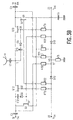
- the transistor T13 mounted as a switch must be non-conducting when the transistor T12 mounted as a switch is conducting.
- a TX signal enters at pole 12 and propagates towards antenna A, or an RX signal comes from antenna A and leaves at pole 13, but the TX and RX signals do not propagate at the same instant.
- a line switching management base In addition, in the telecommunications field, a line switching management base must be able to manage 8 lines or users transmitting or receiving at the same frequency concomitantly by means of a terminal device using such a circuit.
- control signals of the switching transistors T12 and T13 must not be purely and simply in phase opposition, and therefore cannot be generated by complementary clock signals, whereas it is nevertheless necessary that l one of the two transistors T12 or T13 is non-conducting when the other transistor is conducting.
- the transistors T12 and T13 are used to control the bias voltage V TX of the amplifier 40 of the signal transmitter TX on the one hand, and the bias voltage V on the other hand RX of the amplifier 50 of the receiver of the RX signal.
- These two amplifiers 40, 50 necessarily exist in the application described here.
- These bias voltages V RX and V TX are positive and time multiplexed, for example by a microcontroller. The form of these voltages is shown diagrammatically below with reference to the timing diagram in FIG. 2.
- the timing diagram shows, on the one hand the signal V TX and, on the other hand the signal V RX for biasing the amplifiers 40 and 50.
- Each of these signals V TX and V RX shows pulses of length T during which the corresponding bias voltages are used to control the transistors T12 and T13 and turn them on. As these impulses are offset, the switch transistors T12 and T13 are not on at the same time.
- the pulses of each signal V TX and V RX show rising edges separated by a duration of time T which is large compared to the duration ⁇ of a pulse.
- the duration ⁇ of a pulse can be 1/8 of the duration T which separates one pulse from the next.
- the two diodes ⁇ 12 and ⁇ 13, and the resistor R8 constitute a logic circuit 30 with diodes.
- This logic circuit 30 forms an "OR" logic gate used in the switch circuit 20 to obtain the appropriate control voltages to be applied to the control electrodes (grids) of the transistors T12, T13 at using pulsed polarization voltages V TX and V RX .
- the "OR" function is found at node 11.
- the switch circuit 20 shown in FIG. 1B is favorably produced by using field effect transistors of the MESFET type, the pinch voltage of which is negative, of the order of -2V.
- These MESFET transistors are normally conducting in the absence of gate-source voltage, or for a voltage greater than the pinch voltage, and are made non-conducting by a gate-source voltage of value lower than the pinch voltage.
- the field effect transistors T12 and T13 are continuously isolated by the capacitors C2, C3 placed at the input-outputs 12, 13 and by the capacitor C1 placed between the common pole 1 and the antenna A. This makes these transistors floating with respect to ground and therefore to obtain the negative voltage necessary for their pinching, from the positive multiplexed bias voltages generated by means of a positive bias voltage supplied by a standard battery.
- the voltage drop across a diode made using the same technology as the MESFET field effect transistors T12 and T13 is of the order of: V ⁇ ⁇ 0.5 V hence V GS (T12) ⁇ 0.5 V which makes this transistor T12 on.
- this switch circuit 20 is that the appropriate control voltages are generated for the switch transistors T12 and T13, and that at the same time, the DC voltage V D which was necessary for the pole 11 is also generated. This switch circuit 20 therefore does not use other supply voltages than those of the transmitting and receiving amplifiers 40 and 50 already present.
- the diodes D12, D13 and the resistor R'8 constitute a logic circuit 30 with diodes with "OR" function like that of FIG.1A.
- the voltages present at the terminals of the diodes D12, D13 are reported as gate-source control voltages. switch transistors (series transistors) Q12, Q13 respectively.
- This circuit further comprises transistors Q 2 and Q 3 mounted in shunt, the first Q 2 between the input pole 12 and a resistor R2 or R3, and the second Q 3 between the output pole 13 and a resistor R3, the other end of resistors R2 and / or R3 being connected to the second common pole 11 '.
- the transistor Q3 mounted in shunt is controlled in the same way as the transistor Q12 connected in series to be on at the same time.
- the transistor Q2 mounted in shunt is controlled in the same way as the transistor Q13 to be on at the same time.
- the pole 11 ' is connected to the pole 1 through a resistor R'1, and in this case the connections by the resistors R10 and R11 shown in FIG.3A and 3B are deleted.
- the sources of the branch transistors Q2 and Q3 do not are not common, but are connected respectively to the second common pole 11 'by resistors R2 and R3, and are respectively connected to ground by capacitors C'4 and C4.
- the sources of the branched transistors Q 2 and Q 3 are common and connected to the pole 11 'by the only resistor R3 and to the ground through a single capacitor C4.
- the system formed by the transistors Q 2 and Q 3 in shunt, and their biasing means makes it possible to eliminate the residual leakage currents of the transistors in series Q12 and Q13 in the non-conducting state.
- the switch circuit 20 proposed in this second example illustrated by FIGS. 3A, 3B, 3C takes advantage of the use of field effect transistors of the MESFET type having a negative pinch voltage of the order of - 2 V, and can nevertheless operate with a low positive supply voltage by standard battery of the order of 3 to 6 V.
- This switch circuit does not require its own supply voltage. This supply voltage which would have been at the common point 1 of the antenna does not need to be supplied independently by a battery in the present switching circuit.
- the control voltages suitable for the switching transistors Q12 and Q3 on the one hand, and Q13 and Q2 on the other hand, are generated from the bias voltages V TX and V RX already necessarily present in the amplifier circuits 40 and 50 of the transmitter and receiver circuits shown in FIG. 4. These bias voltages are also already time-multiplexed, that is to say shifted cyclically, in relation to the timing diagram of FIG. 2, and their use is therefore particularly advantageous.
- the transistors Q12 and Q3 are on because their gate-source voltages V GS (Q12) and V GS (Q3) equal the drop voltage, approximately 0.5 to 0.7 V in the diode D13 which is then made conductive. This voltage drop V ⁇ in the diode has a level sufficient to make these transistors passable.
- the transistors Q13 and Q2 are non-conducting because their gate-source voltages V GS (Q13) and V GS (Q2) equal the voltage drop, 0.5 to 0.7 in the diode D13 minus the voltage V TX which is of the order of 3 to 6 V. This voltage is therefore sufficiently negative to keep the transistors non-conducting.
- All field effect transistors Q12, Q13, Q2, Q3 mounted as switches are made floating by continuous isolation capacities: C2 and C3 mounted at the input-output poles 12 and 13, C1 mounted between the common pole 1 and the antenna A, C4 mounted between the common sources of the transistors Q2 and Q3 and the ground (FIG.3B), and C4, C'4 mounted between the non-common sources of the transistors Q2 and Q3 and the ground (FIG. 3A and FIG.3C).
- the values of these capacities can be of the order of 100 pF. This floating arrangement makes it possible to obtain the negative control voltages of the transistors from the positive bias voltages.
- the switch circuit (20) is shown used in a mobile telecommunication terminal 100.
- This device also comprises various circuits such as analog-digital, or digital-analog converters, encoders and decoders, adapters, etc., symbolically represented by the block 60 between the microphone 80 and the amplifier 40, and the block 70 between amplifier 50 and speaker 90.
- various circuits such as analog-digital, or digital-analog converters, encoders and decoders, adapters, etc.
- the operating protocol for these systems is of the type referenced TDMA (in English Time Division Multiple Access).
- TDMA Time Division Multiple Access
- the supply voltages supplied by positive batteries of 3 to 6 V are generated in pulsed form, shown in FIG. 2, for example by a microcontroller.
- FIG. 2 the use of telecommunication systems by several users concomitantly is managed by terminals (or bases) distributed geographically over a territory, so that their radius of action covers this territory.
Landscapes
- Engineering & Computer Science (AREA)
- Computer Networks & Wireless Communication (AREA)
- Signal Processing (AREA)
- Transmitters (AREA)
- Waveguide Switches, Polarizers, And Phase Shifters (AREA)
- Transceivers (AREA)
- Electronic Switches (AREA)
Applications Claiming Priority (2)
| Application Number | Priority Date | Filing Date | Title |
|---|---|---|---|
| FR9415873 | 1994-12-29 | ||
| FR9415873 | 1994-12-29 |
Publications (2)
| Publication Number | Publication Date |
|---|---|
| EP0720292A1 true EP0720292A1 (de) | 1996-07-03 |
| EP0720292B1 EP0720292B1 (de) | 2000-03-29 |
Family
ID=9470417
Family Applications (1)
| Application Number | Title | Priority Date | Filing Date |
|---|---|---|---|
| EP95203549A Expired - Lifetime EP0720292B1 (de) | 1994-12-29 | 1995-12-19 | Mobilfunkendgerät mit einem Schaltkreis |
Country Status (4)
| Country | Link |
|---|---|
| US (1) | US5689818A (de) |
| EP (1) | EP0720292B1 (de) |
| JP (1) | JP3456815B2 (de) |
| DE (1) | DE69515979T2 (de) |
Cited By (7)
| Publication number | Priority date | Publication date | Assignee | Title |
|---|---|---|---|---|
| FR2902250A1 (fr) * | 2006-06-12 | 2007-12-14 | Thomson Licensing Sas | Commutateur et dispositif de commutation a isolation selective pour terminaux multimedias |
| EP2613441A1 (de) * | 2012-01-06 | 2013-07-10 | RichWave Technology Corp. | Radiofrequenzschalter, Hilfsspannungserzeugungseinheit für einen Radiofrequenzschalter und Verfahren zum Erhalten von Hilfsspannung für einen Radiofrequenzschalter |
| US9543929B2 (en) | 2012-01-06 | 2017-01-10 | Richwave Technology Corp. | Apparatus and method for obtaining power voltage from control signals |
| US10630287B2 (en) | 2018-08-10 | 2020-04-21 | Richwave Technology Corp. | Radio frequency device and voltage generating circuit thereof |
| US11258445B2 (en) | 2019-10-17 | 2022-02-22 | Richwave Technology Corp. | Radio frequency apparatus and voltage generating device thereof |
| US11290136B2 (en) | 2019-10-16 | 2022-03-29 | Richwave Technology Corp. | Radio frequency device and voltage generating device thereof |
| US11870445B2 (en) | 2020-12-25 | 2024-01-09 | Richwave Technology Corp. | Radio frequency device and voltage generation and harmonic suppressor thereof |
Families Citing this family (15)
| Publication number | Priority date | Publication date | Assignee | Title |
|---|---|---|---|---|
| US6009314A (en) * | 1997-11-17 | 1999-12-28 | Telefonaktiebolaget L/M Ericsson | Monolithic high frequency antenna switch |
| JP2002507074A (ja) * | 1998-03-11 | 2002-03-05 | インフィネオン テクノロジース アクチエンゲゼルシャフト | 移動無線及び移動電話装置のための集積回路 |
| FR2781949B1 (fr) * | 1998-08-03 | 2000-10-27 | St Microelectronics Sa | Dispositif de commutation de signaux radio-frequences |
| DE10102201C2 (de) | 2001-01-18 | 2003-05-08 | Epcos Ag | Elektrisches Schaltmodul, Schaltmodulanordnung und verwendung des Schaltmoduls und der Schaltmodulanordnung |
| JP2003032001A (ja) * | 2001-07-13 | 2003-01-31 | Murata Mfg Co Ltd | 複合高周波スイッチ、高周波モジュール及び通信機 |
| US20050059371A1 (en) * | 2001-09-28 | 2005-03-17 | Christian Block | Circuit arrangement, switching module comprising said circuit arrangement and use of switching module |
| US7492565B2 (en) | 2001-09-28 | 2009-02-17 | Epcos Ag | Bandpass filter electrostatic discharge protection device |
| US7343137B2 (en) * | 2001-09-28 | 2008-03-11 | Epcos Ag | Circuit, switching module comprising the same, and use of said switching module |
| DE60203104D1 (de) * | 2002-06-26 | 2005-04-07 | St Microelectronics Nv | Radiofrequenz-Schalter, insbesondere für ein zellulares Mobiltelefon |
| DE10246098A1 (de) | 2002-10-02 | 2004-04-22 | Epcos Ag | Schaltungsanordnung |
| JP4874887B2 (ja) * | 2007-07-20 | 2012-02-15 | 株式会社東芝 | 高周波半導体スイッチ装置 |
| JP2010050769A (ja) * | 2008-08-22 | 2010-03-04 | New Japan Radio Co Ltd | 半導体スイッチ回路 |
| EP2549655A1 (de) * | 2011-07-21 | 2013-01-23 | Nederlandse Organisatie voor toegepast -natuurwetenschappelijk onderzoek TNO | Hochfrequenzvorrichtung mit einem Sende-/Empfangs-Schaltkreis |
| KR101319731B1 (ko) * | 2012-04-26 | 2013-10-17 | 삼성전기주식회사 | 무선통신 시스템에서의 송수신 신호 스위칭 타임 제어회로 |
| CN114900164A (zh) * | 2022-05-13 | 2022-08-12 | 上海艾为电子技术股份有限公司 | 驱动电路、开关电路及电子设备 |
Citations (6)
| Publication number | Priority date | Publication date | Assignee | Title |
|---|---|---|---|---|
| US4810911A (en) | 1986-11-14 | 1989-03-07 | Nec Corp | FET switch circuit having small insertion loss and exhibiting stable operation |
| US5218285A (en) * | 1991-12-16 | 1993-06-08 | Motorola, Inc. | Electronic device with dual purpose regulator |
| JPH05199094A (ja) * | 1992-01-21 | 1993-08-06 | Sharp Corp | 高周波スイッチ回路 |
| DE4343719A1 (de) * | 1992-12-22 | 1994-06-23 | Murata Manufacturing Co | Hochfrequenzschalter |
| DE4307164A1 (de) * | 1993-03-06 | 1994-09-08 | Constin Design Gmbh | Schnurloses, mobiles Telefon |
| EP0625831A2 (de) * | 1993-05-21 | 1994-11-23 | Sony Corporation | Funksenderempfänger |
Family Cites Families (2)
| Publication number | Priority date | Publication date | Assignee | Title |
|---|---|---|---|---|
| US4399557A (en) * | 1981-12-15 | 1983-08-16 | Motorola Inc. | Minimum power, feedback controller, transmit/receive switch |
| JPS60124146U (ja) * | 1984-01-27 | 1985-08-21 | 日本電気株式会社 | 空中線切換回路 |
-
1995
- 1995-12-19 DE DE69515979T patent/DE69515979T2/de not_active Expired - Fee Related
- 1995-12-19 EP EP95203549A patent/EP0720292B1/de not_active Expired - Lifetime
- 1995-12-21 US US08/576,540 patent/US5689818A/en not_active Expired - Fee Related
- 1995-12-26 JP JP33923895A patent/JP3456815B2/ja not_active Expired - Fee Related
Patent Citations (6)
| Publication number | Priority date | Publication date | Assignee | Title |
|---|---|---|---|---|
| US4810911A (en) | 1986-11-14 | 1989-03-07 | Nec Corp | FET switch circuit having small insertion loss and exhibiting stable operation |
| US5218285A (en) * | 1991-12-16 | 1993-06-08 | Motorola, Inc. | Electronic device with dual purpose regulator |
| JPH05199094A (ja) * | 1992-01-21 | 1993-08-06 | Sharp Corp | 高周波スイッチ回路 |
| DE4343719A1 (de) * | 1992-12-22 | 1994-06-23 | Murata Manufacturing Co | Hochfrequenzschalter |
| DE4307164A1 (de) * | 1993-03-06 | 1994-09-08 | Constin Design Gmbh | Schnurloses, mobiles Telefon |
| EP0625831A2 (de) * | 1993-05-21 | 1994-11-23 | Sony Corporation | Funksenderempfänger |
Non-Patent Citations (1)
| Title |
|---|
| PATENT ABSTRACTS OF JAPAN vol. 17, no. 629 (E - 1462) 19 November 1993 (1993-11-19) * |
Cited By (11)
| Publication number | Priority date | Publication date | Assignee | Title |
|---|---|---|---|---|
| FR2902250A1 (fr) * | 2006-06-12 | 2007-12-14 | Thomson Licensing Sas | Commutateur et dispositif de commutation a isolation selective pour terminaux multimedias |
| EP1868298A3 (de) * | 2006-06-12 | 2008-05-07 | Thomson Licensing S.A. | Schalter und Schaltvorrichtung mit selektiver Isolierung für Multimedia-Endgeräte |
| US7853222B2 (en) | 2006-06-12 | 2010-12-14 | Thomson Licensing | Switch and switching device with selective isolation for multimedia terminals |
| EP2613441A1 (de) * | 2012-01-06 | 2013-07-10 | RichWave Technology Corp. | Radiofrequenzschalter, Hilfsspannungserzeugungseinheit für einen Radiofrequenzschalter und Verfahren zum Erhalten von Hilfsspannung für einen Radiofrequenzschalter |
| CN103219979A (zh) * | 2012-01-06 | 2013-07-24 | 立积电子股份有限公司 | 射频切换器及其辅助电压产生单元和产生辅助电压的方法 |
| US9231578B2 (en) | 2012-01-06 | 2016-01-05 | Richwave Technology Corp. | Apparatus and method for obtaining auxiliary voltage from control signals |
| US9543929B2 (en) | 2012-01-06 | 2017-01-10 | Richwave Technology Corp. | Apparatus and method for obtaining power voltage from control signals |
| US10630287B2 (en) | 2018-08-10 | 2020-04-21 | Richwave Technology Corp. | Radio frequency device and voltage generating circuit thereof |
| US11290136B2 (en) | 2019-10-16 | 2022-03-29 | Richwave Technology Corp. | Radio frequency device and voltage generating device thereof |
| US11258445B2 (en) | 2019-10-17 | 2022-02-22 | Richwave Technology Corp. | Radio frequency apparatus and voltage generating device thereof |
| US11870445B2 (en) | 2020-12-25 | 2024-01-09 | Richwave Technology Corp. | Radio frequency device and voltage generation and harmonic suppressor thereof |
Also Published As
| Publication number | Publication date |
|---|---|
| JPH08293816A (ja) | 1996-11-05 |
| EP0720292B1 (de) | 2000-03-29 |
| JP3456815B2 (ja) | 2003-10-14 |
| DE69515979T2 (de) | 2000-10-05 |
| HK1019021A1 (en) | 2000-01-14 |
| US5689818A (en) | 1997-11-18 |
| DE69515979D1 (de) | 2000-05-04 |
Similar Documents
| Publication | Publication Date | Title |
|---|---|---|
| EP0720292B1 (de) | Mobilfunkendgerät mit einem Schaltkreis | |
| FR3002096A1 (fr) | Dispositif de commutation a corps polarise | |
| EP0660512B1 (de) | Phasenschiebverstärker und seine Verwendung in einer Zusammenführungsschaltung | |
| EP0215707A1 (de) | Spannungsschaltvorrichtung | |
| FR2542548A1 (fr) | Circuit d'interface de ligne telephonique | |
| EP3134972B1 (de) | Leistungsschaltzelle mit normalerweise leitenden feldeffekttransistoren | |
| EP0836271A1 (de) | Integrierter Oszillator und einen solchen Oszillator verwendendes Funktelefon | |
| EP2339744A1 (de) | Niedrigspannungs-Mischschaltung für eine Übertragungsvorrichtung von UWB-Signalen | |
| FR2597280A1 (fr) | Circuit de commutation a large bande commande par un champ electrique | |
| FR2673494A1 (fr) | Module de commutation, matrice de commutateurs et systeme de commutation d'impulsion de grande intensite. | |
| EP0755114B1 (de) | Halbleitervorrichtung mit einem Leistungsverstärker und mobilen Telekommunikationsendgerät mit einer solchen Halbleitervorrichtung | |
| EP0561456A1 (de) | Frequenzsynthetisierer mit schnellem Schaltstromspiegel und Gerät unter Verwendung eines solchen Synthetisierers | |
| FR2538193A1 (fr) | Interface de sortie pour circuit logique a trois etats dans un circuit integre a transistors mos | |
| EP1039652B1 (de) | Antenneanordnung | |
| EP3824549B1 (de) | Architektur für hf-funkfrequenzsender | |
| EP2182631A2 (de) | Mikrowellen-Breitband-Verstärkerzelle mit regelbarer Verstärkung und eine solche Zelle umfassender Verstärker | |
| EP3984135B1 (de) | Kompakter uwb-emitter mit sehr geringem verbrauch und rekonfigurierbarer wellenform | |
| EP0046421B1 (de) | Empfänger für Signalübertragungssystem mittels elektromagnetischer, insbesondere infraroter Strahlung | |
| FR2918523A1 (fr) | Dispositif d'interface pseudo-differentiel avec circuit d'equilibrage | |
| EP1376884B1 (de) | Radiofrequenz-Schalter, insbesondere für ein zellulares Mobiltelefon | |
| WO2004100389A2 (fr) | Dispositif de radiocommunication mettant en oeuvre au moins deux antennes, respectivement pour les radiocommunications et la radiolocalisation et systeme correspondant | |
| FR3062937A1 (fr) | Activation d'un dispositif nfc | |
| EP2457326B1 (de) | Hochfrequenzschalter mit verteilten verstärkern und eingang für ein testsignal | |
| EP1303909B1 (de) | Elektronische signalumsetzungsschaltung und verstärker mit einer solchen schaltung | |
| EP3923477B1 (de) | Vorrichtung zur steuerung eines schalters |
Legal Events
| Date | Code | Title | Description |
|---|---|---|---|
| PUAI | Public reference made under article 153(3) epc to a published international application that has entered the european phase |
Free format text: ORIGINAL CODE: 0009012 |
|
| AK | Designated contracting states |
Kind code of ref document: A1 Designated state(s): DE FR GB |
|
| 17P | Request for examination filed |
Effective date: 19970103 |
|
| GRAG | Despatch of communication of intention to grant |
Free format text: ORIGINAL CODE: EPIDOS AGRA |
|
| 17Q | First examination report despatched |
Effective date: 19990609 |
|
| GRAG | Despatch of communication of intention to grant |
Free format text: ORIGINAL CODE: EPIDOS AGRA |
|
| GRAH | Despatch of communication of intention to grant a patent |
Free format text: ORIGINAL CODE: EPIDOS IGRA |
|
| GRAH | Despatch of communication of intention to grant a patent |
Free format text: ORIGINAL CODE: EPIDOS IGRA |
|
| GRAA | (expected) grant |
Free format text: ORIGINAL CODE: 0009210 |
|
| RAP1 | Party data changed (applicant data changed or rights of an application transferred) |
Owner name: KONINKLIJKE PHILIPS ELECTRONICS N.V. |
|
| AK | Designated contracting states |
Kind code of ref document: B1 Designated state(s): DE FR GB |
|
| REF | Corresponds to: |
Ref document number: 69515979 Country of ref document: DE Date of ref document: 20000504 |
|
| GBT | Gb: translation of ep patent filed (gb section 77(6)(a)/1977) |
Effective date: 20000605 |
|
| PLBE | No opposition filed within time limit |
Free format text: ORIGINAL CODE: 0009261 |
|
| STAA | Information on the status of an ep patent application or granted ep patent |
Free format text: STATUS: NO OPPOSITION FILED WITHIN TIME LIMIT |
|
| 26N | No opposition filed | ||
| REG | Reference to a national code |
Ref country code: GB Ref legal event code: IF02 |
|
| REG | Reference to a national code |
Ref country code: GB Ref legal event code: 746 Effective date: 20020919 |
|
| REG | Reference to a national code |
Ref country code: FR Ref legal event code: D6 |
|
| PGFP | Annual fee paid to national office [announced via postgrant information from national office to epo] |
Ref country code: GB Payment date: 20031224 Year of fee payment: 9 |
|
| PGFP | Annual fee paid to national office [announced via postgrant information from national office to epo] |
Ref country code: FR Payment date: 20031229 Year of fee payment: 9 |
|
| PGFP | Annual fee paid to national office [announced via postgrant information from national office to epo] |
Ref country code: DE Payment date: 20040216 Year of fee payment: 9 |
|
| PG25 | Lapsed in a contracting state [announced via postgrant information from national office to epo] |
Ref country code: GB Free format text: LAPSE BECAUSE OF NON-PAYMENT OF DUE FEES Effective date: 20041219 |
|
| PG25 | Lapsed in a contracting state [announced via postgrant information from national office to epo] |
Ref country code: DE Free format text: LAPSE BECAUSE OF NON-PAYMENT OF DUE FEES Effective date: 20050701 |
|
| GBPC | Gb: european patent ceased through non-payment of renewal fee |
Effective date: 20041219 |
|
| PG25 | Lapsed in a contracting state [announced via postgrant information from national office to epo] |
Ref country code: FR Free format text: LAPSE BECAUSE OF NON-PAYMENT OF DUE FEES Effective date: 20050831 |
|
| REG | Reference to a national code |
Ref country code: FR Ref legal event code: ST |