EP0721935A1 - Organic electroluminescent element and arylenediamine derivative - Google Patents
Organic electroluminescent element and arylenediamine derivative Download PDFInfo
- Publication number
- EP0721935A1 EP0721935A1 EP94927780A EP94927780A EP0721935A1 EP 0721935 A1 EP0721935 A1 EP 0721935A1 EP 94927780 A EP94927780 A EP 94927780A EP 94927780 A EP94927780 A EP 94927780A EP 0721935 A1 EP0721935 A1 EP 0721935A1
- Authority
- EP
- European Patent Office
- Prior art keywords
- group
- layer
- general formula
- derivative
- organic
- Prior art date
- Legal status (The legal status is an assumption and is not a legal conclusion. Google has not performed a legal analysis and makes no representation as to the accuracy of the status listed.)
- Granted
Links
- 0 C*(C)c1cc(C)ccc1C1=CC=CC(C)C=C1 Chemical compound C*(C)c1cc(C)ccc1C1=CC=CC(C)C=C1 0.000 description 3
- NIPLHQMSJSYKTH-UHFFFAOYSA-N CC(CC(C(C)=C1)=[IH])=C1I Chemical compound CC(CC(C(C)=C1)=[IH])=C1I NIPLHQMSJSYKTH-UHFFFAOYSA-N 0.000 description 1
- NQVLOHKMEASTMW-UHFFFAOYSA-N Cc(cc1)ccc1-c(cc1)ccc1N Chemical compound Cc(cc1)ccc1-c(cc1)ccc1N NQVLOHKMEASTMW-UHFFFAOYSA-N 0.000 description 1
- ZDTPCDRWXNSCQQ-UHFFFAOYSA-N Cc(cc1)ccc1-c(cc1)ccc1Nc(cc1)ccc1-c1ccc(C)cc1 Chemical compound Cc(cc1)ccc1-c(cc1)ccc1Nc(cc1)ccc1-c1ccc(C)cc1 ZDTPCDRWXNSCQQ-UHFFFAOYSA-N 0.000 description 1
- JWDOOMYFNAZYDM-UHFFFAOYSA-N Oc(cc1)ccc1-c(cc1)ccc1Nc(cc1)ccc1-c(cc1)ccc1O Chemical compound Oc(cc1)ccc1-c(cc1)ccc1Nc(cc1)ccc1-c(cc1)ccc1O JWDOOMYFNAZYDM-UHFFFAOYSA-N 0.000 description 1
- UJRRIVLIBALCSP-UHFFFAOYSA-N Oc(cc1)ccc1-c(cc1)ccc1Nc(cc1)ccc1-c1ccccc1 Chemical compound Oc(cc1)ccc1-c(cc1)ccc1Nc(cc1)ccc1-c1ccccc1 UJRRIVLIBALCSP-UHFFFAOYSA-N 0.000 description 1
- RPGWZZNNEUHDAQ-UHFFFAOYSA-N Pc1ccccc1 Chemical compound Pc1ccccc1 RPGWZZNNEUHDAQ-UHFFFAOYSA-N 0.000 description 1
Images


Classifications
-
- C—CHEMISTRY; METALLURGY
- C07—ORGANIC CHEMISTRY
- C07C—ACYCLIC OR CARBOCYCLIC COMPOUNDS
- C07C211/00—Compounds containing amino groups bound to a carbon skeleton
- C07C211/43—Compounds containing amino groups bound to a carbon skeleton having amino groups bound to carbon atoms of six-membered aromatic rings of the carbon skeleton
- C07C211/54—Compounds containing amino groups bound to a carbon skeleton having amino groups bound to carbon atoms of six-membered aromatic rings of the carbon skeleton having amino groups bound to two or three six-membered aromatic rings
-
- C—CHEMISTRY; METALLURGY
- C07—ORGANIC CHEMISTRY
- C07C—ACYCLIC OR CARBOCYCLIC COMPOUNDS
- C07C211/00—Compounds containing amino groups bound to a carbon skeleton
- C07C211/43—Compounds containing amino groups bound to a carbon skeleton having amino groups bound to carbon atoms of six-membered aromatic rings of the carbon skeleton
- C07C211/57—Compounds containing amino groups bound to a carbon skeleton having amino groups bound to carbon atoms of six-membered aromatic rings of the carbon skeleton having amino groups bound to carbon atoms of six-membered aromatic rings being part of condensed ring systems of the carbon skeleton
- C07C211/58—Naphthylamines; N-substituted derivatives thereof
-
- C—CHEMISTRY; METALLURGY
- C07—ORGANIC CHEMISTRY
- C07C—ACYCLIC OR CARBOCYCLIC COMPOUNDS
- C07C211/00—Compounds containing amino groups bound to a carbon skeleton
- C07C211/43—Compounds containing amino groups bound to a carbon skeleton having amino groups bound to carbon atoms of six-membered aromatic rings of the carbon skeleton
- C07C211/57—Compounds containing amino groups bound to a carbon skeleton having amino groups bound to carbon atoms of six-membered aromatic rings of the carbon skeleton having amino groups bound to carbon atoms of six-membered aromatic rings being part of condensed ring systems of the carbon skeleton
- C07C211/61—Compounds containing amino groups bound to a carbon skeleton having amino groups bound to carbon atoms of six-membered aromatic rings of the carbon skeleton having amino groups bound to carbon atoms of six-membered aromatic rings being part of condensed ring systems of the carbon skeleton with at least one of the condensed ring systems formed by three or more rings
-
- C—CHEMISTRY; METALLURGY
- C07—ORGANIC CHEMISTRY
- C07C—ACYCLIC OR CARBOCYCLIC COMPOUNDS
- C07C217/00—Compounds containing amino and etherified hydroxy groups bound to the same carbon skeleton
- C07C217/78—Compounds containing amino and etherified hydroxy groups bound to the same carbon skeleton having amino groups and etherified hydroxy groups bound to carbon atoms of six-membered aromatic rings of the same carbon skeleton
- C07C217/80—Compounds containing amino and etherified hydroxy groups bound to the same carbon skeleton having amino groups and etherified hydroxy groups bound to carbon atoms of six-membered aromatic rings of the same carbon skeleton having amino groups and etherified hydroxy groups bound to carbon atoms of non-condensed six-membered aromatic rings
-
- C—CHEMISTRY; METALLURGY
- C07—ORGANIC CHEMISTRY
- C07C—ACYCLIC OR CARBOCYCLIC COMPOUNDS
- C07C217/00—Compounds containing amino and etherified hydroxy groups bound to the same carbon skeleton
- C07C217/78—Compounds containing amino and etherified hydroxy groups bound to the same carbon skeleton having amino groups and etherified hydroxy groups bound to carbon atoms of six-membered aromatic rings of the same carbon skeleton
- C07C217/80—Compounds containing amino and etherified hydroxy groups bound to the same carbon skeleton having amino groups and etherified hydroxy groups bound to carbon atoms of six-membered aromatic rings of the same carbon skeleton having amino groups and etherified hydroxy groups bound to carbon atoms of non-condensed six-membered aromatic rings
- C07C217/82—Compounds containing amino and etherified hydroxy groups bound to the same carbon skeleton having amino groups and etherified hydroxy groups bound to carbon atoms of six-membered aromatic rings of the same carbon skeleton having amino groups and etherified hydroxy groups bound to carbon atoms of non-condensed six-membered aromatic rings of the same non-condensed six-membered aromatic ring
- C07C217/92—Compounds containing amino and etherified hydroxy groups bound to the same carbon skeleton having amino groups and etherified hydroxy groups bound to carbon atoms of six-membered aromatic rings of the same carbon skeleton having amino groups and etherified hydroxy groups bound to carbon atoms of non-condensed six-membered aromatic rings of the same non-condensed six-membered aromatic ring the nitrogen atom of at least one of the amino groups being further bound to a carbon atom of a six-membered aromatic ring
-
- C—CHEMISTRY; METALLURGY
- C09—DYES; PAINTS; POLISHES; NATURAL RESINS; ADHESIVES; COMPOSITIONS NOT OTHERWISE PROVIDED FOR; APPLICATIONS OF MATERIALS NOT OTHERWISE PROVIDED FOR
- C09K—MATERIALS FOR MISCELLANEOUS APPLICATIONS, NOT PROVIDED FOR ELSEWHERE
- C09K11/00—Luminescent materials, e.g. electroluminescent or chemiluminescent
- C09K11/06—Luminescent materials, e.g. electroluminescent or chemiluminescent containing organic luminescent materials
-
- H—ELECTRICITY
- H05—ELECTRIC TECHNIQUES NOT OTHERWISE PROVIDED FOR
- H05B—ELECTRIC HEATING; ELECTRIC LIGHT SOURCES NOT OTHERWISE PROVIDED FOR; CIRCUIT ARRANGEMENTS FOR ELECTRIC LIGHT SOURCES, IN GENERAL
- H05B33/00—Electroluminescent light sources
- H05B33/12—Light sources with substantially two-dimensional [2D] radiating surfaces
- H05B33/14—Light sources with substantially two-dimensional [2D] radiating surfaces characterised by the chemical or physical composition or the arrangement of the electroluminescent material, or by the simultaneous addition of the electroluminescent material in or onto the light source
-
- H—ELECTRICITY
- H10—SEMICONDUCTOR DEVICES; ELECTRIC SOLID-STATE DEVICES NOT OTHERWISE PROVIDED FOR
- H10K—ORGANIC ELECTRIC SOLID-STATE DEVICES
- H10K85/00—Organic materials used in the body or electrodes of devices covered by this subclass
- H10K85/60—Organic compounds having low molecular weight
- H10K85/615—Polycyclic condensed aromatic hydrocarbons, e.g. anthracene
-
- H—ELECTRICITY
- H10—SEMICONDUCTOR DEVICES; ELECTRIC SOLID-STATE DEVICES NOT OTHERWISE PROVIDED FOR
- H10K—ORGANIC ELECTRIC SOLID-STATE DEVICES
- H10K85/00—Organic materials used in the body or electrodes of devices covered by this subclass
- H10K85/60—Organic compounds having low molecular weight
- H10K85/631—Amine compounds having at least two aryl rest on at least one amine-nitrogen atom, e.g. triphenylamine
-
- H—ELECTRICITY
- H10—SEMICONDUCTOR DEVICES; ELECTRIC SOLID-STATE DEVICES NOT OTHERWISE PROVIDED FOR
- H10K—ORGANIC ELECTRIC SOLID-STATE DEVICES
- H10K85/00—Organic materials used in the body or electrodes of devices covered by this subclass
- H10K85/60—Organic compounds having low molecular weight
- H10K85/631—Amine compounds having at least two aryl rest on at least one amine-nitrogen atom, e.g. triphenylamine
- H10K85/633—Amine compounds having at least two aryl rest on at least one amine-nitrogen atom, e.g. triphenylamine comprising polycyclic condensed aromatic hydrocarbons as substituents on the nitrogen atom
-
- C—CHEMISTRY; METALLURGY
- C07—ORGANIC CHEMISTRY
- C07C—ACYCLIC OR CARBOCYCLIC COMPOUNDS
- C07C2601/00—Systems containing only non-condensed rings
- C07C2601/02—Systems containing only non-condensed rings with a three-membered ring
-
- C—CHEMISTRY; METALLURGY
- C07—ORGANIC CHEMISTRY
- C07C—ACYCLIC OR CARBOCYCLIC COMPOUNDS
- C07C2601/00—Systems containing only non-condensed rings
- C07C2601/04—Systems containing only non-condensed rings with a four-membered ring
-
- C—CHEMISTRY; METALLURGY
- C07—ORGANIC CHEMISTRY
- C07C—ACYCLIC OR CARBOCYCLIC COMPOUNDS
- C07C2601/00—Systems containing only non-condensed rings
- C07C2601/06—Systems containing only non-condensed rings with a five-membered ring
- C07C2601/08—Systems containing only non-condensed rings with a five-membered ring the ring being saturated
-
- C—CHEMISTRY; METALLURGY
- C07—ORGANIC CHEMISTRY
- C07C—ACYCLIC OR CARBOCYCLIC COMPOUNDS
- C07C2601/00—Systems containing only non-condensed rings
- C07C2601/12—Systems containing only non-condensed rings with a six-membered ring
- C07C2601/14—The ring being saturated
-
- C—CHEMISTRY; METALLURGY
- C07—ORGANIC CHEMISTRY
- C07C—ACYCLIC OR CARBOCYCLIC COMPOUNDS
- C07C2603/00—Systems containing at least three condensed rings
- C07C2603/02—Ortho- or ortho- and peri-condensed systems
- C07C2603/04—Ortho- or ortho- and peri-condensed systems containing three rings
- C07C2603/06—Ortho- or ortho- and peri-condensed systems containing three rings containing at least one ring with less than six ring members
- C07C2603/10—Ortho- or ortho- and peri-condensed systems containing three rings containing at least one ring with less than six ring members containing five-membered rings
- C07C2603/12—Ortho- or ortho- and peri-condensed systems containing three rings containing at least one ring with less than six ring members containing five-membered rings only one five-membered ring
- C07C2603/18—Fluorenes; Hydrogenated fluorenes
-
- C—CHEMISTRY; METALLURGY
- C07—ORGANIC CHEMISTRY
- C07C—ACYCLIC OR CARBOCYCLIC COMPOUNDS
- C07C2603/00—Systems containing at least three condensed rings
- C07C2603/02—Ortho- or ortho- and peri-condensed systems
- C07C2603/04—Ortho- or ortho- and peri-condensed systems containing three rings
- C07C2603/06—Ortho- or ortho- and peri-condensed systems containing three rings containing at least one ring with less than six ring members
- C07C2603/10—Ortho- or ortho- and peri-condensed systems containing three rings containing at least one ring with less than six ring members containing five-membered rings
- C07C2603/12—Ortho- or ortho- and peri-condensed systems containing three rings containing at least one ring with less than six ring members containing five-membered rings only one five-membered ring
- C07C2603/20—Acenaphthenes; Hydrogenated acenaphthenes
-
- C—CHEMISTRY; METALLURGY
- C07—ORGANIC CHEMISTRY
- C07C—ACYCLIC OR CARBOCYCLIC COMPOUNDS
- C07C2603/00—Systems containing at least three condensed rings
- C07C2603/02—Ortho- or ortho- and peri-condensed systems
- C07C2603/04—Ortho- or ortho- and peri-condensed systems containing three rings
- C07C2603/22—Ortho- or ortho- and peri-condensed systems containing three rings containing only six-membered rings
- C07C2603/24—Anthracenes; Hydrogenated anthracenes
-
- C—CHEMISTRY; METALLURGY
- C07—ORGANIC CHEMISTRY
- C07C—ACYCLIC OR CARBOCYCLIC COMPOUNDS
- C07C2603/00—Systems containing at least three condensed rings
- C07C2603/02—Ortho- or ortho- and peri-condensed systems
- C07C2603/04—Ortho- or ortho- and peri-condensed systems containing three rings
- C07C2603/22—Ortho- or ortho- and peri-condensed systems containing three rings containing only six-membered rings
- C07C2603/26—Phenanthrenes; Hydrogenated phenanthrenes
-
- C—CHEMISTRY; METALLURGY
- C07—ORGANIC CHEMISTRY
- C07C—ACYCLIC OR CARBOCYCLIC COMPOUNDS
- C07C2603/00—Systems containing at least three condensed rings
- C07C2603/02—Ortho- or ortho- and peri-condensed systems
- C07C2603/40—Ortho- or ortho- and peri-condensed systems containing four condensed rings
- C07C2603/42—Ortho- or ortho- and peri-condensed systems containing four condensed rings containing only six-membered rings
- C07C2603/50—Pyrenes; Hydrogenated pyrenes
-
- H—ELECTRICITY
- H10—SEMICONDUCTOR DEVICES; ELECTRIC SOLID-STATE DEVICES NOT OTHERWISE PROVIDED FOR
- H10K—ORGANIC ELECTRIC SOLID-STATE DEVICES
- H10K2102/00—Constructional details relating to the organic devices covered by this subclass
- H10K2102/10—Transparent electrodes, e.g. using graphene
- H10K2102/101—Transparent electrodes, e.g. using graphene comprising transparent conductive oxides [TCO]
- H10K2102/103—Transparent electrodes, e.g. using graphene comprising transparent conductive oxides [TCO] comprising indium oxides, e.g. ITO
-
- H—ELECTRICITY
- H10—SEMICONDUCTOR DEVICES; ELECTRIC SOLID-STATE DEVICES NOT OTHERWISE PROVIDED FOR
- H10K—ORGANIC ELECTRIC SOLID-STATE DEVICES
- H10K50/00—Organic light-emitting devices
- H10K50/10—OLEDs or polymer light-emitting diodes [PLED]
- H10K50/11—OLEDs or polymer light-emitting diodes [PLED] characterised by the electroluminescent [EL] layers
-
- H—ELECTRICITY
- H10—SEMICONDUCTOR DEVICES; ELECTRIC SOLID-STATE DEVICES NOT OTHERWISE PROVIDED FOR
- H10K—ORGANIC ELECTRIC SOLID-STATE DEVICES
- H10K85/00—Organic materials used in the body or electrodes of devices covered by this subclass
- H10K85/30—Coordination compounds
- H10K85/321—Metal complexes comprising a group IIIA element, e.g. Tris (8-hydroxyquinoline) gallium [Gaq3]
- H10K85/324—Metal complexes comprising a group IIIA element, e.g. Tris (8-hydroxyquinoline) gallium [Gaq3] comprising aluminium, e.g. Alq3
-
- H—ELECTRICITY
- H10—SEMICONDUCTOR DEVICES; ELECTRIC SOLID-STATE DEVICES NOT OTHERWISE PROVIDED FOR
- H10K—ORGANIC ELECTRIC SOLID-STATE DEVICES
- H10K85/00—Organic materials used in the body or electrodes of devices covered by this subclass
- H10K85/60—Organic compounds having low molecular weight
- H10K85/615—Polycyclic condensed aromatic hydrocarbons, e.g. anthracene
- H10K85/622—Polycyclic condensed aromatic hydrocarbons, e.g. anthracene containing four rings, e.g. pyrene
-
- H—ELECTRICITY
- H10—SEMICONDUCTOR DEVICES; ELECTRIC SOLID-STATE DEVICES NOT OTHERWISE PROVIDED FOR
- H10K—ORGANIC ELECTRIC SOLID-STATE DEVICES
- H10K85/00—Organic materials used in the body or electrodes of devices covered by this subclass
- H10K85/60—Organic compounds having low molecular weight
- H10K85/615—Polycyclic condensed aromatic hydrocarbons, e.g. anthracene
- H10K85/626—Polycyclic condensed aromatic hydrocarbons, e.g. anthracene containing more than one polycyclic condensed aromatic rings, e.g. bis-anthracene
-
- Y—GENERAL TAGGING OF NEW TECHNOLOGICAL DEVELOPMENTS; GENERAL TAGGING OF CROSS-SECTIONAL TECHNOLOGIES SPANNING OVER SEVERAL SECTIONS OF THE IPC; TECHNICAL SUBJECTS COVERED BY FORMER USPC CROSS-REFERENCE ART COLLECTIONS [XRACs] AND DIGESTS
- Y10—TECHNICAL SUBJECTS COVERED BY FORMER USPC
- Y10S—TECHNICAL SUBJECTS COVERED BY FORMER USPC CROSS-REFERENCE ART COLLECTIONS [XRACs] AND DIGESTS
- Y10S428/00—Stock material or miscellaneous articles
- Y10S428/917—Electroluminescent
Definitions
- the present invention relates to electroluminescence devices (hereinafter, referred to as organic EL devices) and novel arylenediamine derivatives. More particularly, the present invention relates to organic EL devices having a remarkably improved life of light emission by using an arylenediamine derivative as a component thereof, particularly as a material of a hole transporting layer thereof, and novel p-phenylenediamine derivatives and 4,4'-biphenylenediamine derivatives which can remarkably improve the life of light emission of organic EL devices.
- an aromatic tertiary amine is used as the material of a hole transporting layer in an organic EL device having the construction of ITO (Indium Tin Oxide) / a hole transporting layer / a light emitting layer / a cathode (Japanese Patent Application Laid-Open No. Showa 63(1988)-295695), and a high luminance of several hundred cd/m 2 with an applied voltage of 20 V or more has been enabled by the device having this construction.
- ITO Indium Tin Oxide
- a hole transporting layer / a light emitting layer / a cathode Japanese Patent Application Laid-Open No. Showa 63(1988)-295695
- a compound derived by using m-phenylenediamine as the diamine has been disclosed (Japanese Patent Application Laid-Open No. Heisei 5(1993)-105647).
- a sufficient electron-donating property can be expected from this compound because only a phenylene group is present between the two amino groups.
- this compound has a drawback in that this compound has a still higher ionization potential than those of the diamine derivatives described above because the m-phenylenediamine skeleton in this compound cannot have canonical forms, the driving voltage of the EL device therefore cannot be sufficiently decreased, and the life of light emission is short.
- the present invention has an object of providing an organic EL device having a decreased driving voltage or an organic EL device having a remarkably improved life of light emission.
- an organic EL device having a long life of light emission can be obtained by using an arylenediamine derivative having a specific structure as a component of an organic EL device, particularly as a material of a hole transporting layer.
- the present invention provides:
- Figure 1 Figure 1, Figure 2, Figure 3, and Figure 4 show 1 H-NMR spectrum charts of the compounds obtained in Preparation Example 4, Preparation Example 5, Preparation Example 6, and Preparation Example 7, respectively.
- One of the arylenediamine derivatives used in the organic device of the present invention is a compound having 6 or more benzene ring skeletons which is represented by the general formula (I):
- Z represents a phenylene group
- Ar 1 , Ar 2 , Ar 3 , and Ar 4 represent each an aryl group having 6 to 20 carbon atoms.
- Specific examples of the aryl group include phenyl group, naphthyl group, biphenyl group, anthranyl group, acenaphthyl group, phenanthryl group, pyrenyl group, and the like.
- the p-phenylene group represented by Z and the aryl group represented by each of Ar 1 to Ar 4 may each be substituted with alkyl groups having 1 to 6 carbon atoms, such as methyl group, ethyl group, n-propyl group, isopropyl group, cyclopropyl group, n-butyl group, isobutyl group, sec-butyl group, tert-butyl group, cyclobutyl group, n-pentyl group, cyclopentyl group, n-hexyl group, cyclohexyl group, and the like; alkoxy groups having 1 to 6 carbon atoms, such as methoxy group, ethoxy group, n-propoxy group, isopropoxy group, cyclopropoxy group, n-butoxy group, isobutoxy group, sec-butoxy group, tert-butoxy group, cyclobutoxy group, n-pentoxy group, cyclopentoxy group,
- Ar 1 , Ar 2 , Ar 3 , and Ar 4 described above may be the same with each other or different from each other, and the combination of Ar 1 , Ar 2 , Ar 3 , Ar 4 , and Z of the central skeleton must have 6 or more benzene ring skeletons.
- the present inventors have undertaken further studies particularly on the hole transporting layer with the object of improving durability of organic EL devices.
- the life of light emission of an organic EL device can be remarkably increased when, among the p-phenylenediamine derivatives represented by the general formula (I), a p-phenylenediamine derivative having 4 biphenyl groups which is represented by the general formula (II) is used for the hole transporting layer: It has also been discovered that the arylenediamine derivatives used in the organic EL device of the present invention also include 4,4'-biphenylenediamine derivative having 5 biphenyl groups which is represented by the general formula (III): and that durability of an organic EL device can be remarkably increased when the 4,4'-biphenylenediamine derivative is used for a hole transporting layer.
- the diamine derivatives represented by the general formulae (II) and (III) are novel compounds which are not described in literature.
- R 1 to R 17 represent each a hydrogen atom; an alkyl group having 1 to 6 carbon atoms, such as methyl group, ethyl group, n-propyl group, isopropyl group, cyclopropyl group, n-butyl group, isobutyl group, sec-butyl group, tert-butyl group, cyclobutyl group, n-pentyl group, cyclopentyl group, n-hexyl group, cyclohexyl group, or the like; an alkoxy group having 1 to 6 carbon atoms, such as methoxy group, ethoxy group, n-propoxy group, isopropoxy group, cyclopropoxy group, n-butoxy group, isobutoxy group, sec-butoxy group, tert-butoxy group, cyclobutoxy group, n-pentoxy group, cyclopentoxy group, n-hex
- R 1 to R 9 may be the same with each other or different from each other.
- R 1 and R 2 , R 2 and R 4 , R 3 and R 4 , R 5 and R 6 , R 6 and R 8 , R 7 and R 8 , R 2 and R 9 , R 4 and R 9 , R 6 and R 9 , and R 8 and R 9 may each form a ring by being bonded to each other.
- R 10 to R 17 may be the same with each other or different from each other; and R 10 and R 11 , R 11 and R 13 , R 12 and R 13 , R 14 and R 15 , R 15 and R 17 , and R 16 and R 17 , may each form a ring by being bonded to each other.
- the life of light emission of an organic EL device can be remarkably increased by using the p-phenylenediamine derivative represented by the general formula (II) described above or the 4,4'-biphenylenediamine derivative represented by the general formula (III) described above as a component, particularly as a material of a hole transporting layer, of the organic EL device.
- the p-phenylenediamine derivative represented by the general formula (II) can be produced, for example, by the following processes:
- Specific examples of the p-phenylenediamine represented by the general formula (IV) include: Specific examples of the halogenated aryl compound represented by the general formula (V) include: (tBu: t-butyl group; the same in the following formulae) Specific examples of the protected diamine derivative represented by the general formula (VI) include: Specific examples of the amine represented by the general formula (VII) include: Specific examples of the dihalogenated aryl compound represented by the general formula (VIII) include: Specific examples of the halogenated aminoaryl compound represented by the general formula (IX) include: In the process (ii), it is possible that an asymmetric diamine derivative is produced by stepwise removal of the protective groups G and G'.
- a base is used as the base.
- a carbonate, a hydroxide, or a hydride of an alkali metal or an alkaline earth metal, an amine, an alkyllithium, or the like is used. Potassium carbonate is particularly preferable as the base.
- a catalyst can be used if necessary. Examples of the catalyst include copper, salts of copper, nickel, palladium, and the like. As the shape of the catalyst, powder form is preferable. The particle size is preferably in the range of 10 nm to 1 mm, more preferably in the range of 100 to 500 nm.
- the condensation reactions may be conducted in a solid phase without using a solvent or in a solvent. It is more advantageous that the condensation reactions are conducted in a solvent.
- a solvent having a higher boiling point is preferable.
- nitrobenzene, dimethylsulfoxide, dimethylformamide, sulfolane, or the like can be used.
- dimethylsulfoxide is particularly preferable.
- the temperature of the condensation reactions is selected generally in the range of 100 to 400°C, preferably in the range of 150 to 250°C.
- the pressure of the condensation reactions is generally an atmospheric pressure. However, the reactions may be conducted under an elevated pressure if necessary.
- the time of the condensation reactions is varied depending on the types of the materials used, the type of the catalyst, and the temperature. The time is generally about 3 to 36 hours.
- the 4,4'-biphenylenediamine derivative represented by the general formula (III) can be produced, for example, by the following processes:
- Specific examples of the protected diamine derivative represented by the general formula (X) described above include: Specific examples of the halogenated aryl compound represented by the general formula (XI) include: (nPr: n-propyl group; the same in the following formulae), (iPr: isopropyl group; the same in the following formulae), (nBu: n-butyl group; the same in the following formulae), (sBu: sec-butyl group; the same in the following formulae), (nPe: n-pentyl group; the same in the following formulae) (nHex: n-hexyl group; the same in the following formulae)
- Specific examples of the amine represented by the general formula (XII) include: Specific examples of the dihalogenated aryl compound represented by the general formula (XIII) include: Specific examples of the halogenated aminoaryl compound represented by the general formula (XIV) include: In the process (i), it is possible that an asymmetric diamine derivative is produced by step
- an asymmetric diamine derivative is produced by a process including protecting the amino groups in the halogenated aminoaryl compound represented by the general formula (XIV) by protective groups, and subsequently removing the protective groups in separate steps.
- protective group include the same groups described above in the examples of G and G'.
- p-phenylenediamine derivative represented by the general formula (I) described above include the following compounds: Among these compounds, compounds represented by the general formula (I) in which Ar 1 , Ar 2 , Ar 3 , and Ar 4 are each naphthyl group or biphenyl group are preferable.
- the organic EL device of the present invention at least contains the p-phenylenediamine derivative represented by the general formula (I) described above [including the compound represented by the general formula (II) described above] or the 4,4'-biphenylenediamine derivative represented by the general formula (III) described above.
- the diamine derivative may be contained in the organic EL device as a single type or as a combination of two or more types of the diamine derivative.
- the construction of the organic EL device is, for example, (i) an anode / an organic light emitting layer / a cathode, (ii) an anode / a hole transporting layer / an organic light emitting layer / a cathode, (iii) an anode / an organic light emitting layer / an electron injecting layer / a cathode, or (iv) an anode / a hole transporting layer / an organic light emitting layer / an electron injecting layer / a cathode.
- the organic EL device of the present invention may have any of the constructions (i) to (iv) as long as at least one of the layers of compounds placed between a pair of electrodes (an anode and a cathode) [the organic light emitting layer in the device having the construction (i) described above, the hole transporting layer or the organic light emitting layer in the device having the construction (ii), the organic light emitting layer and the electron injecting layer in the device having the construction (iii), and the hole transporting layer, the organic light emitting layer, and the electron injecting layer in the device having the construction (iv)] contains the p-phenylenediamine derivative represented by the general formula (I) described above [including the compound represented by the general formula (II) described above] or the 4,4'-biphenylenediamine derivative represented by the general formula (III).
- the organic EL device having any of these constructions is supported on a substrate.
- the substrate is not particularly limited, and a substrate which is conventionally used in organic EL devices, such as glass, a transparent plastics, quartz, or the like, may be used.
- the layer containing the p-phenylenediamine derivative or the 4,4'-biphenylenediamine derivative which is the characteristic part of the organic EL device of the present invention is preferably a hole transporting layer or an organic light emitting layer, more preferably a hole transporting layer.
- the hole transporting layer containing the p-phenylenediamine derivative or the 4,4'-biphenylenediamine derivative may have a single layer structure consisting of a layer of the p-phenylenediamine derivative or the 4,4'-biphenylenediamine derivative, or a multi-layer structure comprising a layer of the p-phenylenediamine derivative or the 4,4'-biphenylenediamine derivative and a layer of a substance which has conventionally been used as a material of a hole transporting layer of an organic EL device.
- the hole transporting layer may also have a single layer structure consisting of, or a multi-layer structure comprising, a layer of a mixture of the p-phenylenediamine derivative or the 4,4'-biphenylenediamine derivative and a substance which has conventionally been used as a material of a hole transporting layer of an organic EL device.
- the hole transporting layer containing the p-phenylenediamine derivative or the 4,4'-biphenylenediamine derivative can be formed by using the p-phenylenediamine derivative or the 4,4'-biphenylenediamine derivative and other materials for the hole transporting layer, if necessary, by the vacuum vapor deposition method, the casting method, the coating method, the spin coating method, or the like.
- the hole transporting layer may also be formed on a transparent polymer, such as a polycarbonate, a polyurethane, polystyrene, a polyarylate, a polyester, or the like, by the casting method, the coating method, or the spin coating method, using a solution in which the p-phenylenediamine derivative or the 4,4'-biphenylenediamine derivative is dispersed, or by the simultaneous vapor deposition of the p-phenylenediamine derivative or the 4,4'-biphenylenediamine derivative with the transparent polymer.
- a transparent polymer such as a polycarbonate, a polyurethane, polystyrene, a polyarylate, a polyester, or the like
- the organic light emitting layer containing the p-phenylenediamine derivative or the 4,4'-biphenylenediamine derivative may have a single layer structure consisting of a layer of the p-phenylenediamine derivative or the 4,4'-biphenylenediamine derivative, or a multi-layer structure comprising a layer of the p-phenylenediamine derivative or the 4,4'-biphenylenediamine derivative and a layer of a substance which has conventionally been used as a material of an organic light emitting layer of an organic EL device.
- the organic light emitting layer may also have a single layer structure consisting of, or a multi-layer structure comprising, a layer of a mixture of the p-phenylenediamine derivative or the 4,4'-biphenylenediamine derivative and a substance which has conventionally been used as a material of an organic light emitting layer of an organic EL device.
- the organic light emitting layer containing the p-phenylenediamine derivative or the 4,4'-biphenylenediamine derivative can be formed by using the p-phenylenediamine derivative or the 4,4'-biphenylenediamine derivative and other materials for the organic light emitting layer, if necessary, by the vacuum vapor deposition method, the casting method, the coating method, the spin coating method, or the like.
- layers other than the layer containing the p-phenylenediamine derivative or the 4,4'-biphenylenediamine derivative may be formed by using materials which are used in conventional organic EL devices.
- the material of the anode a metal, an alloy, an electric conductive compound, or a mixture of these compounds, which has a great work function (4 eV or more), is preferably used.
- the material of the anode include metals, such as Au and the like; and dielectric transparent materials, such as CuI, ITO, SnO 2 , ZnO, and the like.
- the anode can be prepared by forming a thin layer of the material described above by a method, such as the vapor deposition method, the sputtering method, or the like. When the light emitted from the organic light emitting layer is obtained through the anode, it is preferred that the transmittance of the anode is greater than 10 %.
- the electric resistance of the sheet as the anode is several hundred ⁇ / ⁇ or less.
- the thickness of the anode is selected generally in the range of 10 nm to 1 ⁇ m, preferably in the range of 10 to 200 nm, though the thickness depends on the material used.
- the material of the cathode a metal, an alloy, an electric conductive compound, or a mixture of these compounds, which has a small work function (4 eV or less), is preferably used.
- Specific examples of the material of the cathode include sodium, lithium, a magnesium/copper mixture, Al/Al 2 O 3 , indium, and the like.
- the cathode can be prepared by forming a thin layer of the material described above by a method, such as the vapor deposition method, the sputtering method, or the like. When the light emitted from the organic light emitting layer is obtained through the cathode, it is preferred that the transmittance of the cathode is greater than 10 %.
- the electric resistance of the sheet as the cathode is several hundred ⁇ / ⁇ or less.
- the thickness of the anode is selected generally in the range of 10 nm to 1 ⁇ m, preferably in the range of 50 to 200 nm, though the thickness depends on the material used.
- At least one of the anode and the cathode is formed with a transparent or semi-transparent material.
- the organic light emitting layer in the organic EL device of the present invention is formed with the p-phenylenediamine derivative or the 4,4'-biphenylenediamine derivative and other substances, as the other substance used in addition to the p-phenylenediamine derivative or the 4,4'-biphenylenediamine derivative, for example, a compound which has the property suitable for forming a thin layer, such as a multi-ring condensed aromatic compound, a fluorescent bleaching agent like a benzoxazole bleaching agent, a benzothiazole bleaching agent, a benzimidazole bleaching agent, or the like, a metal chelated oxanoid compound, a distyrylbenzene compound, or the like, can be used.
- a compound which has the property suitable for forming a thin layer such as a multi-ring condensed aromatic compound, a fluorescent bleaching agent like a benzoxazole bleaching agent, a benzothiazole bleaching agent,
- multi-ring condensed aromatic compound described above examples include condensed ring light emitting compounds having a skeleton of anthracene, naphthalene, phenanthrene, pyrene, chrysene, perylene, or the like, and other condensed ring light emitting substances having 8 to 20, preferably 8 condensed rings.
- Examples of the fluorescent bleaching agent described above include compounds disclosed in Japanese Patent Application Laid-Open No. Showa 59(1984)-194393.
- fluorescent bleaching agent examples include benzoxazole bleaching agents, such as 2,5-bis(5,7-di-t-pentyl-2-benzoxazolyl)-1,3,4-thiadiazole, 4,4'-bis(5,7-t-pentyl-2-benzoxazolyl)stilbene, 4,4'-bis(5,7-di(2-methyl-2-butyl)-2-benzoxazolyl) stilbene, 2,5-bis(5,7-di-t-pentyl-2-benzoxazolyl)thiophene, 2,5-bis(5-( ⁇ , ⁇ -dimethylbenzyl)-2-benzoxazolyl)thiophene, 2,5-bis(5,7-di-(2-methyl-2-butyl)-2-bezoxazolyl)3,4-diphenylthiophene, 2,5-bis(5-methyl-2-benzoxazolyl)thiophene, 4,4'-bis(2-benzoxazole)
- metal chelated oxanoid compound described above for example, compounds disclosed in Japanese Patent Application Laid-Open No. Showa 63(1991)-295695 can be used.
- Typical examples of the metal chelated oxanoid compound include metal complexes of 8-hydroxyquinoline derivatives, such as tris(8-quinolinol)aluminum, bis(8-quinolinol)magnesium, bis[benzo(f)-8-quinolinol]zinc, bis(2-methyl-8-quinolinolato)aluminum oxide, tris(8-quinolinol)indium, tris(5-methyl-8-quinolinol)aluminum, 8-quinolinollithium, tris(5-chloro-8-quinolinol)gallium, bis(5-chloro-8-quinolinol)calcium, poly(zinc(II)-bis(8-hydroxy-5-quinolinonyl)methane); dilith
- distyrylbenzene compound described above for example, compounds disclosed in European Patent No. 0373582 can be used.
- Specific examples of the distyrylbenzene compound include 1,4-bis(2-methylstyryl)benzene, 1,4-bis(3-methylstyryl)benzene, 1,4-bis(4-methylstyryl)benzene, distyrylbenzene, 1,4-bis(2-ethylstyryl)benzene, 1,4-bis(3-ethylstyryl)benzene, 1,4-bis(2-methylstyryl)-2-methylbenzene, 1,4-bis(2-methylstyryl)-2-ethylbenzene, and the like.
- the distyrylpyrazine derivatives disclosed in Japanese Patent Application Laid-Open No. Heisei 2(1990)-252793 can also be used as the material of the organic light emitting layer.
- Typical examples of the distyrylpyrazine derivative include 2,5-bis(4-methylstyryl)pyrazine, 2,5-bis(4-ethylstyryl)pyrazine, 2,5-bis[2-(1-naphthyl)vinyl]pyrazine, 2,5-bis(4-methoxystyryl)pyrazine, 2,5-bis[2-(4-biphenyl)vinyl]pyrazine, 2,5-bis[2-(1-pyrenyl)vinyl]pyrazine, and the like.
- Dimethylidine derivatives disclosed in European Patent No. 0388768 and Japanese Patent Application Laid-Open No. Heisei 3(1991)-231970 can also be used as the material of the organic light emitting layer.
- Typical examples of the dimethylidine derivative include 1,4-phenylenedimethylidine, 4,4'-biphenylenedimethylidine, 2,5-xylylenedimethylidine, 2,6-naphthylenedimethylidine, 1,4-biphenylenedimethylidine, 1,4-p-terephenylenedimethylidine, 9,10-anthracenediyldimethylidine, 4,4'-(2,2-di-t-butylphenylvinyl)biphenyl, 4,4'-(2,2-diphenylvinyl)biphenyl, like other compounds, and derivatives of these compounds.
- coumarine derivatives disclosed in Japanese Patent Application Laid-Open No. Heisei 2(1990)-191694, perylene derivatives disclosed in Japanese Patent Application Laid-Open No. Heisei 2(1990)-196885, naphthalene derivatives disclosed in Japanese Patent Application Laid-Open No. Heisei 2(1990)-255789, phthaloperynone derivatives disclosed in Japanese Patent Application Laid-Open No. Heisei 2(1990)-289676 and Japanese Patent Application Laid-Open No. Heisei 2(1990)-88689, and styrylamine derivatives disclosed in Japanese Patent Application Laid-Open No. Heisei 2(1990)-250292, can also be used as the material of the light emitting layer.
- the material of the organic light emitting layer is selected from these compounds in accordance with the desired color of the emitted light and other desired properties.
- the organic light emitting layer of the organic EL device of the present invention may also be formed by additionally using a fluorescent substance as described in United States Patent No. 4,769,292.
- the substance which is used as the base material in this case may be the p-phenylenediamine derivative, the 4,4'-biphenylenediamine derivative, or a material of the light emitting layer other than the p-phenylenediamine derivative and the 4,4'-biphenylenediamine derivative.
- the substance may also be a mixture of the p-phenylenediamine derivative or the 4,4'-biphenylenediamine derivative and a material of the organic light emitting layer.
- the organic light emitting layer is formed by additionally using a fluorescent substance, it is preferred that the amount of the additionally used fluorescent substance is several percent by mol or less.
- the fluorescent substance emits light in response with the recombination of an electron and a hole, and carries a part of the light emitting function.
- a compound which does not have the property of forming a thin layer may also be used.
- Specific examples of such a compound include 1,4-diphenyl-1,3-butadiene, 1,1,4,4-tetraphenyl-1,3-butadiene, tetraphenylcyclopentadiene, and the like.
- an organic EL device prepared by using the above-described material which does not have the property of forming a thin layer has a drawback in that the life of the device is short.
- the hole transporting layer which is used, if necessary, in the organic EL device of the present invention may be a layer containing the p-phenylenediamine derivative or the 4,4'-biphenylenediamine derivative, or a layer containing none of the p-phenylenediamine derivative and the 4,4'-biphenylenediamine derivative as long as the organic light emitting layer contains the p-phenylenediamine derivative or the 4,4'-biphenylenediamine derivative.
- the material of the hole transporting layer other than the p-phenylenediamine derivative or the 4,4'-biphenylenediamine derivative various types of substance which have conventionally been used as a material of a hole transporting layer of an organic EL device can be used.
- the hole transporting layer may have, as described above, a single layer structure consisting of a layer of the p-phenylenediamine derivative or the 4,4'-biphenylenediamine derivative, a multi-layer structure comprising a layer of the p-phenylenediamine derivative or the 4,4'-biphenylenediamine derivative and a layer of a substance which has conventionally been used as a material of a hole transporting layer of an organic EL device.
- the hole transporting layer may also have a single layer structure consisting of, or a multi-layer structure comprising, a layer of a mixture of the p-phenylenediamine derivative or the 4,4'-biphenylenediamine derivative and a substance which has conventionally been used as a material of a hole transporting layer of an organic EL device.
- the preferable layer structures among these structures are the single layer structure consisting of a layer of the p-phenylenediamine derivative or the 4,4'-biphenylenediamine derivative, and a multi-layer structure comprising a layer of the p-phenylenediamine derivative or a layer of the 4,4'-biphenylenediamine derivative and a layer of a porphylin compound (such as a compound disclosed in Japanese Patent Application Laid-Open No. Showa 63(1988)-295695, or the like), or a layer of an organic semi-conductive oligomer.
- a porphylin compound such as a compound disclosed in Japanese Patent Application Laid-Open No. Showa 63(1988)-295695, or the like
- porphylin compound examples include porphin, 5,10,15,20-tetraphenyl-21H-,23H-porphin copper (II), 5,10,15,20-tetraphenyl-21H-,23H-porphin zinc (II), 5,10,15,20-tetrakis(perfluorophenyl)-21H-,23H-porphin, silicon phthalocyanine oxide, aluminum phthalocyanine chloride, phthalocyanine (no metal), dilithium phthalocyanine, copper tetramethylphthalocyanine, copper phthalocyanine, chromium phthalocyanine, zinc phthalocyanine, lead phthalocyanine, titanium phthalocyanine oxide, magnesium phthalocyanine, copper octamethylphthalocyanine, and the like.
- any type of compound can be selected from conventional electron transporting compounds and used as the material of the electron injecting layer as long as the layer has the function of transporting the electron injected from the cathode to the organic light emitting layer.
- the electron injecting layer is the layer having any of the electron injecting property, the electron transporting property, and the electron barrier property, and the compounds (98) to (102) described above as well as crystalline or amorphous materials derived from Si, SiC, CdS, or the like, may be used for forming the layer.
- the organic EL device of the present invention may also have a layer for improving adhesion between the layers in addition to the anode, the cathode, the organic light emitting layer, the hole transporting layer formed if necessary, and the electron injecting layer formed if necessary.
- a layer for improving adhesion between the organic light emitting layer and the cathode include metal complex compounds derived from quinolinol, such as tris(8-quinolinol)aluminum, tris(8-quinolinol)indium, and the like.
- the organic EL device of the present invention described above can be produced by a process such as one of the following processes in accordance with the construction of the device.
- An anode is prepared on a suitable substrate by forming a thin layer made of a desired electrode material, such as an anode material, in such a manner that the thickness of the layer is 1 ⁇ m or less, preferably in the range of 10 to 200 nm, by a method, such as the vapor deposition method, the sputtering method, or the like. Then, an organic light emitting layer is formed on the anode thus prepared by forming a thin layer of the p-phenylenediamine derivative or the 4,4'-biphenylenediamine derivative.
- a desired electrode material such as an anode material
- the formation of the thin layer of the p-phenylenediamine derivative or the 4,4'-biphenylenediamine derivative can be conducted by a method, such as the vacuum vapor deposition method, the spin coating method, the casting method, or the like.
- the vacuum vapor deposition method is preferable because a uniform thin film is more easily obtained and possibility of formation of pin-holes is smaller.
- the conditions of the vacuum vapor deposition are varied depending on the type of the p-phenylenediamine derivative or the 4,4'-biphenylenediamine derivative, and the crystal structure and the association structure of the organic light emitting layer which is to be formed.
- the heating temperature of a boat is suitably selected in the range of 50 to 400°C
- the degree of vacuum is suitably selected in the range of 10 -6 to 10 -3 Pa
- the rate of vapor deposition is suitably selected in the range of 0.01 to 50 nm/sec
- the temperature of the substrate is suitably selected in the range of -50 to +300°C
- the thickness of the film is suitably selected in the range of 5 nm to 5 ⁇ m.
- a cathode is prepared on the organic light emitting layer thus formed by forming a thin layer made of a material of the cathode in such a manner that the thickness of the layer is 1 ⁇ m or less, preferably in the range of 10 to 200 nm, by a method, such as the vapor deposition method, the sputtering method, or the like.
- the desired organic EL device can be obtained by the process described above. It is possible in this process for preparation of the organic EL device that the order of the preparation of layers is reversed, and a cathode, an organic light emitting layer, and an anode are formed on a substrate in this order.
- An anode is prepared on a suitable substrate by the same procedures as those used in (a) described above. Then, an organic light emitting layer is formed on the anode thus prepared by coating the anode with a solution containing a material of the hole transporting layer, a material of the organic light emitting layer, a material of the electron injecting layer, a binder (polyvinylcarbozole or the like), and the like materials.
- a cathode is prepared by forming a thin layer made of a material of the cathode on the organic light emitting layer by the same procedures as those used in (a) described above.
- the desired organic EL device can be obtained by the process described above.
- An organic light emitting layer having a multi-layer structure may be prepared by forming a layer of a thin layer of a desired material of the organic light emitting layer on the layer formed in the above by a method, such as the vapor deposition method.
- the organic light emitting layer may also be formed by simultaneous vapor deposition of the material of the organic light emitting layer, the material of the hole transporting layer, and the material of the electron injecting layer.
- An anode is prepared on a suitable substrate by the same procedures as those used in (a) described above.
- a hole transporting layer is formed on the anode thus prepared by forming a thin layer of the p-phenylenediamine derivative or the 4,4'-biphenylenediamine derivative.
- the formation of the hole transporting layer can be conducted by the same procedures as those used in the formation of the organic light emitting layer (containing the p-phenylenediamine derivative or the 4,4'-biphenylenediamine derivative) in (a) described above.
- an organic light emitting layer is formed on the hole transporting layer by using a desired material of the organic light emitting layer.
- the organic light emitting layer can be formed by preparing a thin layer of the material of the light emitting layer using a method, such as the vacuum vapor deposition method, the spin coating method, the casting method, or the like. Among these methods, the vacuum vapor deposition method is preferable because a uniform thin layer is more easily obtained and possibility of formation of pin-holes is smaller.
- a cathode is prepared by forming a thin layer made of a material of the cathode on the organic light emitting layer by the same procedures as those used in (a) described above.
- the desired organic EL device can be obtained by the process described above.
- An anode, a hole transporting layer (containing the p-phenylenediamine derivative or the 4,4'-biphenylenediamine derivative), and an organic light emitting layer are formed on a suitable substrate by the same procedures as those used in (c).
- an electron injecting layer is formed by forming a thin layer made of an electron transporting compound on the organic light emitting layer in such a manner that the thickness of the layer is 1 ⁇ m or less, preferably in the range of 5 to 100 nm, by a method, such as the vapor deposition method, the sputtering method, or the like.
- a cathode is prepared by forming a thin layer made of a material of the cathode on the prepared electron injecting layer by the same procedures as those used in (c) described above.
- the desired organic EL device can be prepared by the process described above.
- the organic EL device of the present invention which can be prepared as described above emits light by applying a direct voltage of 5 to 40 V in the condition that the anode is connected to a positive electrode (+) and the cathode is connected to a negative electrode (-). When the connection is reversed, no electric current is observed and no light is emitted at all.
- an alternating voltage is applied to the organic EL device, light emission is observed only in the condition that the polarity of the anode is positive and the polarity of the cathode is negative.
- any type of wave shape can be used.
- the organic EL device of the present invention is an organic EL device in which at least one of the layers of compound, which have a single layer structure or a multi-layer structure and at least contain an organic light emitting layer, contains a p-phenylenediamine derivative having 6 or more benzene ring skeletons, or an organic EL device in which at least one of the layers of compound, which have a single layer structure or a multi-layer structure and at least contain an organic light emitting layer, contains the 4,4'-biphenylenediamine derivative having 5 or more biphenyl group.
- the organic EL device has an improved life of light emission and very excellent durability
- a 300 ml flask of an egg-plant shape was charged with 3.42 g (13.2 mmol) of N,N'-diphenyl-1,4-phenylenediamine [a product of Kanto Kagaku Co., Ltd.], 9.35 g (33.4 mmol) of 4-iododiphenyl [a product of Nard Kenkyusho], 5.22 g (37.8 mmol) of anhydrous calcium carbonate, and 1 g (16 mmol) of copper powder.
- DMSO dimethylsulfoxide
- the extract was dried with anhydrous sodium sulfate, and the solvent was removed in a vacuum from the dried extract by using an evaporator.
- the obtained compound was purified by using a column packed with Wakogel C-200 (a product of Hiroshima Wako Co., Ltd.) with toluene used as the developing solvent, to obtain 2.53 g of a light yellow powder.
- a 300 ml flask of an egg-plant shape was charged with 5.02 g (13.9 mmol) of N,N'-di-(2-naphthyl)-1,4-phenylenediamine [a product of Kanto Kagaku Co., Ltd.], 8.25 g (40.4 mmol) of 4-iodobenzene [a product of Tokyo Kasei Co., Ltd.], 6.84 g (49.6 mmol) of anhydrous calcium carbonate, and 1 g (16 mmol) of copper powder.
- the mixture was suspended in 300 ml of DMSO, and was allowed to react at 180°C for 5 hours.
- a 300 ml flask of an egg-plant shape was charged with 2.13 g (5.92 mmol) of N,N'-di-(2-naphthyl)-1,4-phenylenediamine [a product of Kanto Kagaku Co., Ltd.], 4.70 g (16.8 mmol) of 4-iododiphenyl [a product of Nard Kenkyusho], 3.19 g (23.3 mmol) of anhydrous calcium carbonate, and 1 g (16 mmol) of copper powder.
- the mixture was suspended in 300 ml of DMSO, and was allowed to react at 180°C for 5 hours.
- a 300 ml flask of an egg-plant shape was charged with 1.00 g (9.26 mmol) of 1,4-phenylenediamine [a product of Tokyo Kasei Co., Ltd.], 11.0 g (39.3 mmol) of 4-iododiphenyl [a product of Nard Kenkyusho], 12.2 g (88.4 mmol) of anhydrous calcium carbonate, and 1 g (16 mmol) of copper powder.
- the mixture was suspended in 200 ml of dimethylsulfoxide (DMSO), and was allowed to react at 180°C for 5 hours. Then, inorganic components were removed by filtration, and the filtrate was extracted with methylene chloride.
- DMSO dimethylsulfoxide
- the extract was dried with anhydrous sodium sulfate, and the solvent was removed in a vacuum from the dried extract by using an evaporator.
- the obtained compound was purified by using a column packed with Wakogel C-200 (a product of Hiroshima Wako Co., Ltd.) with toluene used as the developing solvent, to obtain 1.4 g of a light yellow powder.
- a 300 ml flask of an egg-plant shape was charged with 0.50 g (4.63 mmol) of 1,4-phenylenediamine [a product of Tokyo Kasei Co., Ltd.], 6.68 g (22.7 mmol) of 4-methyl-4-iododiphenyl [a product of Nard Kenkyusho], 5 g (36 mmol) of anhydrous calcium carbonate, and 1 g (16 mmol) of copper powder.
- the mixture was suspended in 200 ml of DMSO, and was allowed to react at 180°C for 5 hours. Then, inorganic components were removed by filtration, and the filtrate was extracted with methylene chloride.
- the extract was dried with anhydrous sodium sulfate, and the solvent was removed in a vacuum from the dried extract by using an evaporator.
- the obtained compound was purified by using a column packed with Wakogel C-200 (a product of Hiroshima Wako Co., Ltd.) with toluene used as the developing solvent, to obtain 0.40 g of a light yellow powder.
- a 300 ml flask of an egg-plant shape was charged with 5.03 g (18.8 mmol) of N,N'-diacetyl-4,4'-benzidine [a product of Tokyo Kasei Co., Ltd.], 12.3 g (43.8 mmol) of 4-iododiphenyl, 11 g (80 mmol) of anhydrous calcium carbonate, and 1 g (16 mmol) of copper powder.
- the mixture was suspended in 200 ml of DMSO, and was allowed to react at 180°C for 5 hours. Then, inorganic components were removed by filtration, and the filtrate was extracted with methylene chloride. The extract was dried with anhydrous sodium sulfate, and the solvent was removed in a vacuum from the dried extract by using an evaporator.
- the remaining product was dissolved in 500 ml of tetrahyrofuran (THF), and 50 ml of an aqueous solution prepared by dissolving 20 g of potassium hydroxide and 300 of ethanol were added to the THF solution.
- the hydrolysis was allowed to proceed by heating the solution for 5 hours under stirring in a 1 liter flask.
- the reaction product was extracted with ethyl acetate, and the extract was dried with anhydrous sodium sulfate.
- the obtained compound was purified by using a column packed with Wakogel C-200 (a product of Hiroshima Wako Co., Ltd.) with methylene chloride used as the developing solvent, to obtain 9.3 g of an intermediate product as an ocher powder.
- a 300 ml three-necked flask was charged with 1.02 g (2.09 mmol) of the intermediate product, 1.54 g (5.50 mmol) of 4-iododiphenyl, 1.99 g (14.4 mmol) of anhydrous potassium carbonate, and 1 g (16 mmol) of copper powder.
- the mixture was suspended in 200 ml of DMSO, and was allowed to react at 180°C for 5 hours. Then, inorganic components were removed by filtration, and the filtrate was extracted with methylene chloride.
- the extract was dried with anhydrous sodium sulfate, and the solvent was removed in a vacuum from the dried extract by using an evaporator.
- the obtained compound was purified by using a column packed with Wakogel C-200 (a product of Hiroshima Wako Co., Ltd.) with toluene used as the developing solvent, to obtain 0.50 g of a light yellow powder.
- a coated plate prepared by coating an ITO electrode on a glass substrate of 25 mm ⁇ 75 mm ⁇ 1.1 mm to the thickness of 100 nm was used as the transparent supporting substrate.
- the prepared transparent supporting substrate was cleaned with isopropyl alcohol under ultrasonic wave.
- the cleaned supporting substrate was fixed to a substrate holder of a vacuum vapor deposition system [a product of Nippon Shinku Gijutsu Co., Ltd.].
- a vacuum vapor deposition system [a product of Nippon Shinku Gijutsu Co., Ltd.].
- MTDATA tris(3-methylphenylphenylamino)triphenylamine
- Compound (1) obtained in Preparation Example 1 was placed in another electrically heated boat made of molybdenum.
- DPVBi 4,4'-bis(2,2-diphenylvinyl)biphenyl
- the boat containing MTDATA was heated, and a film of MTDATA was prepared on the ITO electrode to the thickness of 60 nm at a rate of 0.1 to 0.3 nm/sec. Then, the boat containing Compound (1) was heated, and a hole transporting layer of 20 nm thickness was prepared by accumulating Compound (1) at a rate of vapor deposition of 0.1 to 0.3 nm/sec. Subsequently, DPVBi was laminated on the prepared hole transporting layer to the thickness of 40 nm by vapor deposition from still another boat to prepare a light emitting layer. The rate of vapor deposition was 0.1 to 0.2 nm/min.
- Alq tris(8-quinolinol)aluminum
- the obtained plate was taken out from the vacuum chamber, and after placing a mask made of stainless steel on the above-obtained injection layer, the plate was again fixed to the substrate holder.
- a tungsten basket 0.5 g of silver wire was placed, and 1 g of magnesium ribbon was placed in a boat of molybdenum.
- the pressure in the vacuum chamber was decreased to 1 ⁇ 10 -4 Pa, and magnesium and silver were simultaneously vapor deposited at the rates of 1.8 nm/sec and 0.1 nm/sec, respectively, to prepare a cathode.
- a device was prepared by the same procedures as those used in Example 1 except that Compound (2) obtained in Preparation Example 2 was used as the material of the hole transporting layer in place of Compound (1) obtained in Preparation Example 1 which was used in Example 1.
- a device was prepared by the same procedures as those used in Example 1 except that Compound (3) obtained in Preparation Example 3 was used as the material of the hole transporting layer in place of Compound (1) obtained in Preparation Example 1 which was used in Example 1.
- a device was prepared by the same procedures as those used in Example 1 except that Compound (27) obtained in Preparation Example 4 was used as the material of the hole transporting layer in place of Compound (1) obtained in Preparation Example 1 which was used in Example 1.
- a device was prepared by the same procedures as those used in Example 1 except that Compound (28) obtained in Preparation Example 5 was used as the material of the hole transporting layer in place of Compound (1) obtained in Preparation Example 1 which was used in Example 1.
- a device was prepared by the same procedures as those used in Example 1 except that Compound (61) obtained in Preparation Example 6 was used as the material of the hole transporting layer in place of Compound (1) obtained in Preparation Example 1 which was used in Example 1.
- a device was prepared by the same procedures as those used in Example 1 except that Compound (62) obtained in Preparation Example 7 was used as the material of the hole transporting layer in place of Compound (1) obtained in Preparation Example 1 which was used in Example 1.
- a device was prepared by the same procedures as those used in Example 1 except that N,N'-diphenyl-N,N'-bis(3-methylphenyl)-1,1'-biphenyl-4,4'-diamine (TPD) was used as the material of the hole transporting layer in place of Compound (1) obtained in Preparation Example 1 which was used in Example 1.
- TPD N,N'-diphenyl-N,N'-bis(3-methylphenyl)-1,1'-biphenyl-4,4'-diamine
- a device was prepared by the same procedures as those used in Example 1 except that N,N,N',N'-tetraphenyl-p-phenylenediamine was used as the material of the hole transporting layer in place of Compound (1) obtained in Preparation Example 1 which was used in Example 1.
- a device was prepared by the same procedures as those used in Example 1 except that N,N,N',N'-tetrakis-(4-biphenyl)-m-phenylenediamine was used as the material of the hole transporting layer in place of Compound (1) obtained in Preparation Example 1 which was used in Example 1.
- a device was prepared by the same procedures as those used in Example 1 except that N,N,N',N'-tetrakis-(4-biphenyl)-3,3'-dimethyl-4,4'-benzidine was used as the material of the hole transporting layer in place of Compound (1) obtained in Preparation Example 1 which was used in Example 1.
- the life of light emission is the time passed for each device from the start of light emission with the initial luminance of 100 cd/m 2 to the time when the luminance decreased to 50 cd/m 2 which is a half of the initial value, while the device is driven by a constant current.
- the devices of Examples 1 to 7 had very remarkably improved lives of light emission in comparison with that of the device using TPD (Comparative Example 1) which is the hole transporting material showing the longest life of light emission among conventional materials.
- N,N,N',N'-Tetraphenyl-p-phenylenediamine used in Comparative Example 2 is a conventional hole transporting material. This material has high crystallizability because this material has only 5 benzene rings in the molecule, and dielectric breakdown occurred during the measurement of the life of light emission. In contrast, compounds used in Examples 1 to 7 did not show crystallization at all because they all have 6 or more benzene rings in the molecule, and uniform films could be maintained for a long time.
- N,N,N',N'-Tetrakis-(4-biphenyl)-m-phenylenediamine used in Comparative Example 3 also has 6 or more benzene rings in the molecule, and no problem arose with respect to formation and maintenance of a thin layer. However, the life of light emission was found to be very short.
- N,N,N',N'-Tetrakis-(4-biphenyl)-3,3'-dimethyl-4,4'-benzidine used in Comparative Example 4 also has 6 or more benzene rings in the molecule, and no problem arose with respect to formation and maintenance of a thin layer. However, the life of light emission was found to be very short.
- the organic EL device of the present invention contains a p-phenylenediamine derivative or a 4,4'-biphenylenediamine derivative as a component thereof, and has the characteristics that the life of light emission is improved and that the durability is excellent.
- the arylenediamine derivative of the present invention can remarkably improve the life of light emission of an organic EL device.
Landscapes
- Chemical & Material Sciences (AREA)
- Organic Chemistry (AREA)
- Engineering & Computer Science (AREA)
- Materials Engineering (AREA)
- Physics & Mathematics (AREA)
- Spectroscopy & Molecular Physics (AREA)
- Electroluminescent Light Sources (AREA)
- Organic Low-Molecular-Weight Compounds And Preparation Thereof (AREA)
- Luminescent Compositions (AREA)
- Low-Molecular Organic Synthesis Reactions Using Catalysts (AREA)
Abstract
Description
- The present invention relates to electroluminescence devices (hereinafter, referred to as organic EL devices) and novel arylenediamine derivatives. More particularly, the present invention relates to organic EL devices having a remarkably improved life of light emission by using an arylenediamine derivative as a component thereof, particularly as a material of a hole transporting layer thereof, and novel p-phenylenediamine derivatives and 4,4'-biphenylenediamine derivatives which can remarkably improve the life of light emission of organic EL devices.
- As for the construction of organic EL devices, various types have heretofore been known. It has been disclosed that an aromatic tertiary amine is used as the material of a hole transporting layer in an organic EL device having the construction of ITO (Indium Tin Oxide) / a hole transporting layer / a light emitting layer / a cathode (Japanese Patent Application Laid-Open No. Showa 63(1988)-295695), and a high luminance of several hundred cd/m2 with an applied voltage of 20 V or more has been enabled by the device having this construction. Furthermore, it has been disclosed that, by using TPD [N,N'-diphenyl-N,N'-bis(3-methylphenyl)-1,1'-biphenyl-4,4'-diamine] as the aromatic tertiary amine, a luminance of 100 cd/m2 can be obtained with an applied voltage of 8 V even in the case of blue light emission (Japanese Patent Application Laid-Open No. Heisei 3(1991)-231970). However, the above-disclosed diamine derivative has a drawback in that contribution of canonical forms is weak because the two amino groups are located at positions separate from each other, and the diamine derivative has a high ionization potential. Therefore, the driving voltage of the EL device cannot be sufficiently decreased, and the device furthermore has a half-life period of several ten hours. Thus, the device described above does not have a sufficient property for practical application.
- A compound derived by using m-phenylenediamine as the diamine has been disclosed (Japanese Patent Application Laid-Open No. Heisei 5(1993)-105647). A sufficient electron-donating property can be expected from this compound because only a phenylene group is present between the two amino groups. However, this compound has a drawback in that this compound has a still higher ionization potential than those of the diamine derivatives described above because the m-phenylenediamine skeleton in this compound cannot have canonical forms, the driving voltage of the EL device therefore cannot be sufficiently decreased, and the life of light emission is short.
- When application of an EL device to a flat panel display or the like is considered, it is necessary that the life of light emission be improved. It has been disclosed in Japanese Patent Application Laid-Open No. Heisei 5(1993)-107758 that a triamine compound can be used as a material of charge transport in an EL device. However, this compound cannot sufficiently satisfy the requirements described above.
- Under the situation described above, the present invention has an object of providing an organic EL device having a decreased driving voltage or an organic EL device having a remarkably improved life of light emission.
- As the result of extensive studies undertaken by the present inventors to develop the organic EL device having the desirable properties described above, it has been discovered that an organic EL device having a long life of light emission can be obtained by using an arylenediamine derivative having a specific structure as a component of an organic EL device, particularly as a material of a hole transporting layer.
- It has also been discovered by the present inventors that, among the arylenediamine derivatives described above, compounds having some types of structure, p-phenylenediamine derivatives having specific structures, and 4,4'-biphenylenediamine having specific structures are novel compounds which are not described in literature, and that an organic EL device having a remarkably improved life of light emission can be obtained by using these compounds as a component of an organic EL device, particularly as a material of a hole transporting layer. The present invention has been completed on the basis of the above discoveries.
- Thus, the present invention provides:
- (1) An organic electroluminescence device at least containing a p-phenylenediamine derivative having 6 or more benzene ring skeletons which is represented by the general formula (I):

- (2) A p-phenylenediamine derivative represented by the general formula (II):

- (3) An organic electroluminescence device at least containing a p-phenylenediamine derivative represented by the general formula (II);
- (4) A 4,4'-biphenylenediamine derivative represented by the general formula (III):

- (5) An organic electroluminescence device at least containing a 4,4'-biphenylenediamine derivative represented by the general formula (III).
- Figure 1, Figure 2, Figure 3, and Figure 4 show 1H-NMR spectrum charts of the compounds obtained in Preparation Example 4, Preparation Example 5, Preparation Example 6, and Preparation Example 7, respectively.
- One of the arylenediamine derivatives used in the organic device of the present invention is a compound having 6 or more benzene ring skeletons which is represented by the general formula (I):

In the general formula (I) described above, Z represents a phenylene group, and Ar1, Ar2, Ar3, and Ar4 represent each an aryl group having 6 to 20 carbon atoms. Specific examples of the aryl group include phenyl group, naphthyl group, biphenyl group, anthranyl group, acenaphthyl group, phenanthryl group, pyrenyl group, and the like. The p-phenylene group represented by Z and the aryl group represented by each of Ar1 to Ar4 may each be substituted with alkyl groups having 1 to 6 carbon atoms, such as methyl group, ethyl group, n-propyl group, isopropyl group, cyclopropyl group, n-butyl group, isobutyl group, sec-butyl group, tert-butyl group, cyclobutyl group, n-pentyl group, cyclopentyl group, n-hexyl group, cyclohexyl group, and the like; alkoxy groups having 1 to 6 carbon atoms, such as methoxy group, ethoxy group, n-propoxy group, isopropoxy group, cyclopropoxy group, n-butoxy group, isobutoxy group, sec-butoxy group, tert-butoxy group, cyclobutoxy group, n-pentoxy group, cyclopentoxy group, n-hexoxy group, cyclohexoxy group, and the like; or phenyl groups. - Ar1, Ar2, Ar3, and Ar4 described above may be the same with each other or different from each other, and the combination of Ar1, Ar2, Ar3, Ar4, and Z of the central skeleton must have 6 or more benzene ring skeletons.
- The present inventors have undertaken further studies particularly on the hole transporting layer with the object of improving durability of organic EL devices.
- As the result of the studies, it has been discovered that the life of light emission of an organic EL device can be remarkably increased when, among the p-phenylenediamine derivatives represented by the general formula (I), a p-phenylenediamine derivative having 4 biphenyl groups which is represented by the general formula (II) is used for the hole transporting layer:

It has also been discovered that the arylenediamine derivatives used in the organic EL device of the present invention also include 4,4'-biphenylenediamine derivative having 5 biphenyl groups which is represented by the general formula (III):
and that durability of an organic EL device can be remarkably increased when the 4,4'-biphenylenediamine derivative is used for a hole transporting layer. The diamine derivatives represented by the general formulae (II) and (III) are novel compounds which are not described in literature. - In the general formulae (II) and (III), R1 to R17 represent each a hydrogen atom; an alkyl group having 1 to 6 carbon atoms, such as methyl group, ethyl group, n-propyl group, isopropyl group, cyclopropyl group, n-butyl group, isobutyl group, sec-butyl group, tert-butyl group, cyclobutyl group, n-pentyl group, cyclopentyl group, n-hexyl group, cyclohexyl group, or the like; an alkoxy group having 1 to 6 carbon atoms, such as methoxy group, ethoxy group, n-propoxy group, isopropoxy group, cyclopropoxy group, n-butoxy group, isobutoxy group, sec-butoxy group, tert-butoxy group, cyclobutoxy group, n-pentoxy group, cyclopentoxy group, n-hexoxy group, cyclohexoxy group, or the like; or a phenyl group.
- In the general formula (II), R1 to R9 may be the same with each other or different from each other. R1 and R2, R2 and R4, R3 and R4, R5 and R6, R6 and R8, R7 and R8, R2 and R9, R4 and R9, R6 and R9, and R8 and R9, may each form a ring by being bonded to each other.
- In general formula (III), R10 to R17 may be the same with each other or different from each other; and R10 and R11, R11 and R13, R12 and R13, R14 and R15, R15 and R17, and R16 and R17, may each form a ring by being bonded to each other.
- The life of light emission of an organic EL device can be remarkably increased by using the p-phenylenediamine derivative represented by the general formula (II) described above or the 4,4'-biphenylenediamine derivative represented by the general formula (III) described above as a component, particularly as a material of a hole transporting layer, of the organic EL device.
- Processes for producing the p-phenylenediamine derivative represented by the general formula (II) described above and the 4,4'-biphenylenediamine derivative represented by the general formula (III) described above are described in the following.
- The p-phenylenediamine derivative represented by the general formula (II) can be produced, for example, by the following processes:
- (i) A process comprising condensing a p-phenylenediamine represented by the general formula (IV):


- (ii) A process comprising condensing a protected diamine derivative represented by the general formula (VI):

- (iii) A process comprising condensing an amine represented by the general formula (VII):


- (iv) A process comprising condensing the amine represented by the general formula (VII) described above, a halogenated aminoaryl compound represented by the general formula (IX):

- Specific examples of the p-phenylenediamine represented by the general formula (IV) include:

Specific examples of the halogenated aryl compound represented by the general formula (V) include:
(tBu: t-butyl group; the same in the following formulae)
Specific examples of the protected diamine derivative represented by the general formula (VI) include:
Specific examples of the amine represented by the general formula (VII) include:

Specific examples of the dihalogenated aryl compound represented by the general formula (VIII) include:
Specific examples of the halogenated aminoaryl compound represented by the general formula (IX) include:
In the process (ii), it is possible that an asymmetric diamine derivative is produced by stepwise removal of the protective groups G and G'. - In the condensation reactions (i) to (iv) described above, a base is used. As the base, for example, a carbonate, a hydroxide, or a hydride of an alkali metal or an alkaline earth metal, an amine, an alkyllithium, or the like, is used. Potassium carbonate is particularly preferable as the base. In the condensation reactions, a catalyst can be used if necessary. Examples of the catalyst include copper, salts of copper, nickel, palladium, and the like. As the shape of the catalyst, powder form is preferable. The particle size is preferably in the range of 10 nm to 1 mm, more preferably in the range of 100 to 500 nm. The condensation reactions may be conducted in a solid phase without using a solvent or in a solvent. It is more advantageous that the condensation reactions are conducted in a solvent. In this case, a solvent having a higher boiling point is preferable. For example, nitrobenzene, dimethylsulfoxide, dimethylformamide, sulfolane, or the like can be used. Among these solvents, dimethylsulfoxide is particularly preferable.
- The temperature of the condensation reactions is selected generally in the range of 100 to 400°C, preferably in the range of 150 to 250°C. The pressure of the condensation reactions is generally an atmospheric pressure. However, the reactions may be conducted under an elevated pressure if necessary. The time of the condensation reactions is varied depending on the types of the materials used, the type of the catalyst, and the temperature. The time is generally about 3 to 36 hours.
- The 4,4'-biphenylenediamine derivative represented by the general formula (III) can be produced, for example, by the following processes:
- (i) A process comprising condensing a protected diamine derivative represented by the general formula (X):


- (ii) A process comprising condensing an amine represented by the general formula (XII):


- (iii) A process comprising condensing an amine represented by the general formula (XII) described above and a halogenated aminoaryl compound represented by the general formula (XIV):

- Specific examples of the protected diamine derivative represented by the general formula (X) described above include:

Specific examples of the halogenated aryl compound represented by the general formula (XI) include:

(nPr: n-propyl group; the same in the following formulae),
(iPr: isopropyl group; the same in the following formulae),

(nBu: n-butyl group; the same in the following formulae),
(sBu: sec-butyl group; the same in the following formulae),
(nPe: n-pentyl group; the same in the following formulae)
(nHex: n-hexyl group; the same in the following formulae)

Specific examples of the amine represented by the general formula (XII) include:
Specific examples of the dihalogenated aryl compound represented by the general formula (XIII) include:
Specific examples of the halogenated aminoaryl compound represented by the general formula (XIV) include:
In the process (i), it is possible that an asymmetric diamine derivative is produced by stepwise removal of the protective groups G and G'. - In the process (iii), it is possible that an asymmetric diamine derivative is produced by a process including protecting the amino groups in the halogenated aminoaryl compound represented by the general formula (XIV) by protective groups, and subsequently removing the protective groups in separate steps. Examples of the protective group include the same groups described above in the examples of G and G'.
- The conditions in the condensation reactions (i) to (iii) are the same as those in the processes for producing the p-phenylenediamine derivative represented by the general formula (II) described above.
- Specific examples of the p-phenylenediamine derivative represented by the general formula (I) described above include the following compounds:


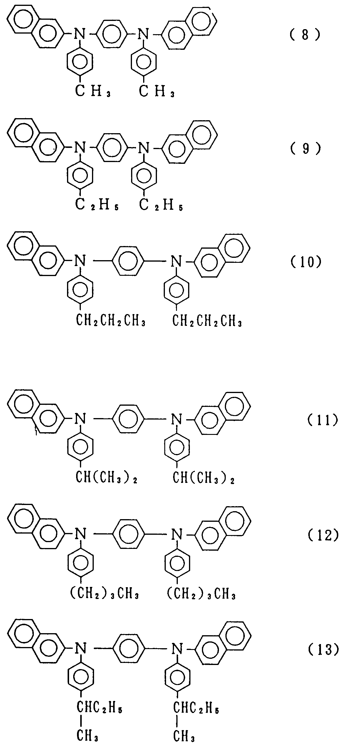


Among these compounds, compounds represented by the general formula (I) in which Ar1, Ar2, Ar3, and Ar4 are each naphthyl group or biphenyl group are preferable. - Specific examples of the p-phenylenediamine derivative represented by the general formula (II) described above include the following compounds:


Specific examples of the 4,4'-biphenylenediamine derivative represented by the general formula (III) include the following compounds:


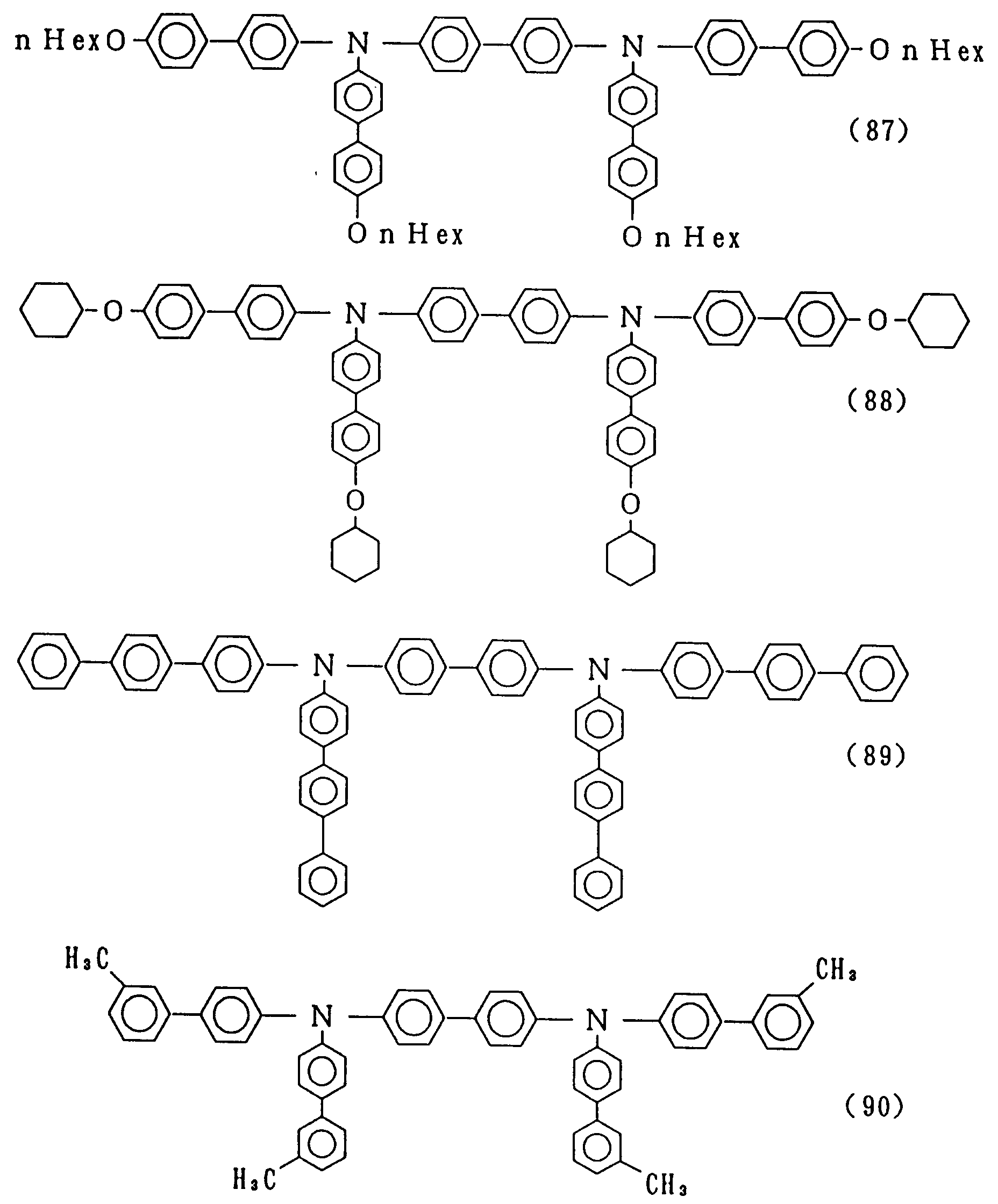


The organic EL device of the present invention at least contains the p-phenylenediamine derivative represented by the general formula (I) described above [including the compound represented by the general formula (II) described above] or the 4,4'-biphenylenediamine derivative represented by the general formula (III) described above. The diamine derivative may be contained in the organic EL device as a single type or as a combination of two or more types of the diamine derivative. - The construction of the organic EL device is, for example, (i) an anode / an organic light emitting layer / a cathode, (ii) an anode / a hole transporting layer / an organic light emitting layer / a cathode, (iii) an anode / an organic light emitting layer / an electron injecting layer / a cathode, or (iv) an anode / a hole transporting layer / an organic light emitting layer / an electron injecting layer / a cathode. The organic EL device of the present invention may have any of the constructions (i) to (iv) as long as at least one of the layers of compounds placed between a pair of electrodes (an anode and a cathode) [the organic light emitting layer in the device having the construction (i) described above, the hole transporting layer or the organic light emitting layer in the device having the construction (ii), the organic light emitting layer and the electron injecting layer in the device having the construction (iii), and the hole transporting layer, the organic light emitting layer, and the electron injecting layer in the device having the construction (iv)] contains the p-phenylenediamine derivative represented by the general formula (I) described above [including the compound represented by the general formula (II) described above] or the 4,4'-biphenylenediamine derivative represented by the general formula (III). It is preferred that the organic EL device having any of these constructions is supported on a substrate. The substrate is not particularly limited, and a substrate which is conventionally used in organic EL devices, such as glass, a transparent plastics, quartz, or the like, may be used.
- The layer containing the p-phenylenediamine derivative or the 4,4'-biphenylenediamine derivative which is the characteristic part of the organic EL device of the present invention is preferably a hole transporting layer or an organic light emitting layer, more preferably a hole transporting layer.
- The hole transporting layer containing the p-phenylenediamine derivative or the 4,4'-biphenylenediamine derivative may have a single layer structure consisting of a layer of the p-phenylenediamine derivative or the 4,4'-biphenylenediamine derivative, or a multi-layer structure comprising a layer of the p-phenylenediamine derivative or the 4,4'-biphenylenediamine derivative and a layer of a substance which has conventionally been used as a material of a hole transporting layer of an organic EL device. The hole transporting layer may also have a single layer structure consisting of, or a multi-layer structure comprising, a layer of a mixture of the p-phenylenediamine derivative or the 4,4'-biphenylenediamine derivative and a substance which has conventionally been used as a material of a hole transporting layer of an organic EL device.
- The hole transporting layer containing the p-phenylenediamine derivative or the 4,4'-biphenylenediamine derivative can be formed by using the p-phenylenediamine derivative or the 4,4'-biphenylenediamine derivative and other materials for the hole transporting layer, if necessary, by the vacuum vapor deposition method, the casting method, the coating method, the spin coating method, or the like. The hole transporting layer may also be formed on a transparent polymer, such as a polycarbonate, a polyurethane, polystyrene, a polyarylate, a polyester, or the like, by the casting method, the coating method, or the spin coating method, using a solution in which the p-phenylenediamine derivative or the 4,4'-biphenylenediamine derivative is dispersed, or by the simultaneous vapor deposition of the p-phenylenediamine derivative or the 4,4'-biphenylenediamine derivative with the transparent polymer.
- The organic light emitting layer containing the p-phenylenediamine derivative or the 4,4'-biphenylenediamine derivative may have a single layer structure consisting of a layer of the p-phenylenediamine derivative or the 4,4'-biphenylenediamine derivative, or a multi-layer structure comprising a layer of the p-phenylenediamine derivative or the 4,4'-biphenylenediamine derivative and a layer of a substance which has conventionally been used as a material of an organic light emitting layer of an organic EL device. The organic light emitting layer may also have a single layer structure consisting of, or a multi-layer structure comprising, a layer of a mixture of the p-phenylenediamine derivative or the 4,4'-biphenylenediamine derivative and a substance which has conventionally been used as a material of an organic light emitting layer of an organic EL device. The organic light emitting layer containing the p-phenylenediamine derivative or the 4,4'-biphenylenediamine derivative can be formed by using the p-phenylenediamine derivative or the 4,4'-biphenylenediamine derivative and other materials for the organic light emitting layer, if necessary, by the vacuum vapor deposition method, the casting method, the coating method, the spin coating method, or the like.
- In the organic EL device of the present invention, layers other than the layer containing the p-phenylenediamine derivative or the 4,4'-biphenylenediamine derivative may be formed by using materials which are used in conventional organic EL devices.
- For example, as the material of the anode, a metal, an alloy, an electric conductive compound, or a mixture of these compounds, which has a great work function (4 eV or more), is preferably used. Specific examples of the material of the anode include metals, such as Au and the like; and dielectric transparent materials, such as CuI, ITO, SnO2, ZnO, and the like. The anode can be prepared by forming a thin layer of the material described above by a method, such as the vapor deposition method, the sputtering method, or the like. When the light emitted from the organic light emitting layer is obtained through the anode, it is preferred that the transmittance of the anode is greater than 10 %. It is also preferred that the electric resistance of the sheet as the anode is several hundred Ω/□ or less. The thickness of the anode is selected generally in the range of 10 nm to 1 µm, preferably in the range of 10 to 200 nm, though the thickness depends on the material used.
- On the other hand, as the material of the cathode, a metal, an alloy, an electric conductive compound, or a mixture of these compounds, which has a small work function (4 eV or less), is preferably used. Specific examples of the material of the cathode include sodium, lithium, a magnesium/copper mixture, Al/Al2O3, indium, and the like. The cathode can be prepared by forming a thin layer of the material described above by a method, such as the vapor deposition method, the sputtering method, or the like. When the light emitted from the organic light emitting layer is obtained through the cathode, it is preferred that the transmittance of the cathode is greater than 10 %. It is also preferred that the electric resistance of the sheet as the cathode is several hundred Ω/□ or less. The thickness of the anode is selected generally in the range of 10 nm to 1 µm, preferably in the range of 50 to 200 nm, though the thickness depends on the material used.
- In view of efficiently obtaining the light emitted from the organic light emitting layer, it is preferred that at least one of the anode and the cathode is formed with a transparent or semi-transparent material.
- When the organic light emitting layer in the organic EL device of the present invention is formed with the p-phenylenediamine derivative or the 4,4'-biphenylenediamine derivative and other substances, as the other substance used in addition to the p-phenylenediamine derivative or the 4,4'-biphenylenediamine derivative, for example, a compound which has the property suitable for forming a thin layer, such as a multi-ring condensed aromatic compound, a fluorescent bleaching agent like a benzoxazole bleaching agent, a benzothiazole bleaching agent, a benzimidazole bleaching agent, or the like, a metal chelated oxanoid compound, a distyrylbenzene compound, or the like, can be used.
- Specific examples of the multi-ring condensed aromatic compound described above include condensed ring light emitting compounds having a skeleton of anthracene, naphthalene, phenanthrene, pyrene, chrysene, perylene, or the like, and other condensed ring light emitting substances having 8 to 20, preferably 8 condensed rings.
- Examples of the fluorescent bleaching agent described above, such as a benzoxazole bleaching agent, a benzothiazole bleaching agent, a benzimidazole bleaching agent, or the like, include compounds disclosed in Japanese Patent Application Laid-Open No. Showa 59(1984)-194393. Typical examples of the fluorescent bleaching agent include benzoxazole bleaching agents, such as 2,5-bis(5,7-di-t-pentyl-2-benzoxazolyl)-1,3,4-thiadiazole, 4,4'-bis(5,7-t-pentyl-2-benzoxazolyl)stilbene, 4,4'-bis(5,7-di(2-methyl-2-butyl)-2-benzoxazolyl) stilbene, 2,5-bis(5,7-di-t-pentyl-2-benzoxazolyl)thiophene, 2,5-bis(5-(α,α-dimethylbenzyl)-2-benzoxazolyl)thiophene, 2,5-bis(5,7-di-(2-methyl-2-butyl)-2-bezoxazolyl)3,4-diphenylthiophene, 2,5-bis(5-methyl-2-benzoxazolyl)thiophene, 4,4'-bis(2-benzoxazolyl)biphenyl, 5-methyl-2-(2-(4-(5-methyl-2-benzoxazolyl)phenyl)vinyl)benzoxazol, 2-(2-(4-chlorophenyl)vinyl)naphtho(1,2-d)oxazol, and the like; benzothiazole bleaching agents, such as 2,2'-(p-phenylenedivinylene)-bisbenzothiazole, and the like; and benzimidazole bleaching agents, such as 2-(2-(4-carboxylphenyl)vinyl)benzimidazole, and the like.
- As the metal chelated oxanoid compound described above, for example, compounds disclosed in Japanese Patent Application Laid-Open No. Showa 63(1991)-295695 can be used. Typical examples of the metal chelated oxanoid compound include metal complexes of 8-hydroxyquinoline derivatives, such as tris(8-quinolinol)aluminum, bis(8-quinolinol)magnesium, bis[benzo(f)-8-quinolinol]zinc, bis(2-methyl-8-quinolinolato)aluminum oxide, tris(8-quinolinol)indium, tris(5-methyl-8-quinolinol)aluminum, 8-quinolinollithium, tris(5-chloro-8-quinolinol)gallium, bis(5-chloro-8-quinolinol)calcium, poly(zinc(II)-bis(8-hydroxy-5-quinolinonyl)methane); dilithium epindolidione; and the like.
- As the distyrylbenzene compound described above, for example, compounds disclosed in European Patent No. 0373582 can be used. Specific examples of the distyrylbenzene compound include 1,4-bis(2-methylstyryl)benzene, 1,4-bis(3-methylstyryl)benzene, 1,4-bis(4-methylstyryl)benzene, distyrylbenzene, 1,4-bis(2-ethylstyryl)benzene, 1,4-bis(3-ethylstyryl)benzene, 1,4-bis(2-methylstyryl)-2-methylbenzene, 1,4-bis(2-methylstyryl)-2-ethylbenzene, and the like.
- The distyrylpyrazine derivatives disclosed in Japanese Patent Application Laid-Open No. Heisei 2(1990)-252793 can also be used as the material of the organic light emitting layer. Typical examples of the distyrylpyrazine derivative include 2,5-bis(4-methylstyryl)pyrazine, 2,5-bis(4-ethylstyryl)pyrazine, 2,5-bis[2-(1-naphthyl)vinyl]pyrazine, 2,5-bis(4-methoxystyryl)pyrazine, 2,5-bis[2-(4-biphenyl)vinyl]pyrazine, 2,5-bis[2-(1-pyrenyl)vinyl]pyrazine, and the like.
- Dimethylidine derivatives disclosed in European Patent No. 0388768 and Japanese Patent Application Laid-Open No. Heisei 3(1991)-231970 can also be used as the material of the organic light emitting layer. Typical examples of the dimethylidine derivative include 1,4-phenylenedimethylidine, 4,4'-biphenylenedimethylidine, 2,5-xylylenedimethylidine, 2,6-naphthylenedimethylidine, 1,4-biphenylenedimethylidine, 1,4-p-terephenylenedimethylidine, 9,10-anthracenediyldimethylidine, 4,4'-(2,2-di-t-butylphenylvinyl)biphenyl, 4,4'-(2,2-diphenylvinyl)biphenyl, like other compounds, and derivatives of these compounds.
- Furthermore, coumarine derivatives disclosed in Japanese Patent Application Laid-Open No. Heisei 2(1990)-191694, perylene derivatives disclosed in Japanese Patent Application Laid-Open No. Heisei 2(1990)-196885, naphthalene derivatives disclosed in Japanese Patent Application Laid-Open No. Heisei 2(1990)-255789, phthaloperynone derivatives disclosed in Japanese Patent Application Laid-Open No. Heisei 2(1990)-289676 and Japanese Patent Application Laid-Open No. Heisei 2(1990)-88689, and styrylamine derivatives disclosed in Japanese Patent Application Laid-Open No. Heisei 2(1990)-250292, can also be used as the material of the light emitting layer.
- The material of the organic light emitting layer is selected from these compounds in accordance with the desired color of the emitted light and other desired properties. The organic light emitting layer of the organic EL device of the present invention may also be formed by additionally using a fluorescent substance as described in United States Patent No. 4,769,292. The substance which is used as the base material in this case may be the p-phenylenediamine derivative, the 4,4'-biphenylenediamine derivative, or a material of the light emitting layer other than the p-phenylenediamine derivative and the 4,4'-biphenylenediamine derivative. The substance may also be a mixture of the p-phenylenediamine derivative or the 4,4'-biphenylenediamine derivative and a material of the organic light emitting layer. When the organic light emitting layer is formed by additionally using a fluorescent substance, it is preferred that the amount of the additionally used fluorescent substance is several percent by mol or less. The fluorescent substance emits light in response with the recombination of an electron and a hole, and carries a part of the light emitting function.
- As the material of the organic light emitting layer, a compound which does not have the property of forming a thin layer may also be used. Specific examples of such a compound include 1,4-diphenyl-1,3-butadiene, 1,1,4,4-tetraphenyl-1,3-butadiene, tetraphenylcyclopentadiene, and the like. However, an organic EL device prepared by using the above-described material which does not have the property of forming a thin layer has a drawback in that the life of the device is short.
- The hole transporting layer which is used, if necessary, in the organic EL device of the present invention may be a layer containing the p-phenylenediamine derivative or the 4,4'-biphenylenediamine derivative, or a layer containing none of the p-phenylenediamine derivative and the 4,4'-biphenylenediamine derivative as long as the organic light emitting layer contains the p-phenylenediamine derivative or the 4,4'-biphenylenediamine derivative. As the material of the hole transporting layer other than the p-phenylenediamine derivative or the 4,4'-biphenylenediamine derivative, various types of substance which have conventionally been used as a material of a hole transporting layer of an organic EL device can be used.
- When a layer containing the p-phenylenediamine derivative or the 4,4'-biphenylenediamine derivative is formed as the hole transporting layer which is formed in the organic EL device of the present invention if necessary, the hole transporting layer may have, as described above, a single layer structure consisting of a layer of the p-phenylenediamine derivative or the 4,4'-biphenylenediamine derivative, a multi-layer structure comprising a layer of the p-phenylenediamine derivative or the 4,4'-biphenylenediamine derivative and a layer of a substance which has conventionally been used as a material of a hole transporting layer of an organic EL device. The hole transporting layer may also have a single layer structure consisting of, or a multi-layer structure comprising, a layer of a mixture of the p-phenylenediamine derivative or the 4,4'-biphenylenediamine derivative and a substance which has conventionally been used as a material of a hole transporting layer of an organic EL device. The preferable layer structures among these structures are the single layer structure consisting of a layer of the p-phenylenediamine derivative or the 4,4'-biphenylenediamine derivative, and a multi-layer structure comprising a layer of the p-phenylenediamine derivative or a layer of the 4,4'-biphenylenediamine derivative and a layer of a porphylin compound (such as a compound disclosed in Japanese Patent Application Laid-Open No. Showa 63(1988)-295695, or the like), or a layer of an organic semi-conductive oligomer.
- Typical examples of the porphylin compound include porphin, 5,10,15,20-tetraphenyl-21H-,23H-porphin copper (II), 5,10,15,20-tetraphenyl-21H-,23H-porphin zinc (II), 5,10,15,20-tetrakis(perfluorophenyl)-21H-,23H-porphin, silicon phthalocyanine oxide, aluminum phthalocyanine chloride, phthalocyanine (no metal), dilithium phthalocyanine, copper tetramethylphthalocyanine, copper phthalocyanine, chromium phthalocyanine, zinc phthalocyanine, lead phthalocyanine, titanium phthalocyanine oxide, magnesium phthalocyanine, copper octamethylphthalocyanine, and the like.
- As the organic semi-conductive oligomer described above, a compound represented by the general formula (XV):

wherein R18, R19, and R20 represent each an alkyl group having 1 to 10 carbon atoms, an alkoxy group having 1 to 10 carbon atoms, or cyclohexyl group, and may be the same with each other or different from each other, k, m, and n represent each an integer of 1 to 3, and the sum of k, m, and n is 5 or less, is particularly preferable. - In the electron injecting layer (the electron injecting and transporting layer) formed in the organic EL device of the present invention if necessary, any type of compound can be selected from conventional electron transporting compounds and used as the material of the electron injecting layer as long as the layer has the function of transporting the electron injected from the cathode to the organic light emitting layer.
- Examples of the preferable electron transporting compound include compounds having the following formulae:

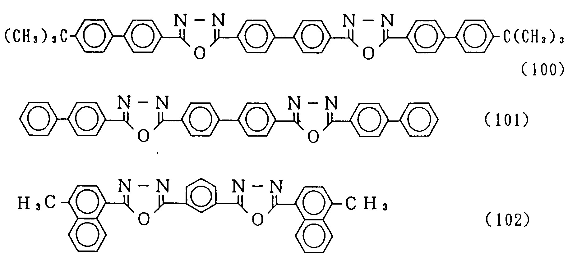
The electron injecting layer is the layer having any of the electron injecting property, the electron transporting property, and the electron barrier property, and the compounds (98) to (102) described above as well as crystalline or amorphous materials derived from Si, SiC, CdS, or the like, may be used for forming the layer. - The organic EL device of the present invention may also have a layer for improving adhesion between the layers in addition to the anode, the cathode, the organic light emitting layer, the hole transporting layer formed if necessary, and the electron injecting layer formed if necessary. Specific examples of the material used for such a layer, for example a layer for improving adhesion between the organic light emitting layer and the cathode, include metal complex compounds derived from quinolinol, such as tris(8-quinolinol)aluminum, tris(8-quinolinol)indium, and the like.
- The organic EL device of the present invention described above can be produced by a process such as one of the following processes in accordance with the construction of the device.
- An anode is prepared on a suitable substrate by forming a thin layer made of a desired electrode material, such as an anode material, in such a manner that the thickness of the layer is 1 µm or less, preferably in the range of 10 to 200 nm, by a method, such as the vapor deposition method, the sputtering method, or the like. Then, an organic light emitting layer is formed on the anode thus prepared by forming a thin layer of the p-phenylenediamine derivative or the 4,4'-biphenylenediamine derivative. The formation of the thin layer of the p-phenylenediamine derivative or the 4,4'-biphenylenediamine derivative can be conducted by a method, such as the vacuum vapor deposition method, the spin coating method, the casting method, or the like. Among these methods, the vacuum vapor deposition method is preferable because a uniform thin film is more easily obtained and possibility of formation of pin-holes is smaller.
- When the vacuum vapor deposition method is conducted for forming a thin layer of the p-phenylenediamine derivative or the 4,4'-biphenylenediamine derivative, the conditions of the vacuum vapor deposition are varied depending on the type of the p-phenylenediamine derivative or the 4,4'-biphenylenediamine derivative, and the crystal structure and the association structure of the organic light emitting layer which is to be formed. It is generally preferred that the heating temperature of a boat is suitably selected in the range of 50 to 400°C, the degree of vacuum is suitably selected in the range of 10-6 to 10-3 Pa, the rate of vapor deposition is suitably selected in the range of 0.01 to 50 nm/sec, the temperature of the substrate is suitably selected in the range of -50 to +300°C, and the thickness of the film is suitably selected in the range of 5 nm to 5 µm.
- After the organic light emitting layer is formed as described above, a cathode is prepared on the organic light emitting layer thus formed by forming a thin layer made of a material of the cathode in such a manner that the thickness of the layer is 1 µm or less, preferably in the range of 10 to 200 nm, by a method, such as the vapor deposition method, the sputtering method, or the like. The desired organic EL device can be obtained by the process described above. It is possible in this process for preparation of the organic EL device that the order of the preparation of layers is reversed, and a cathode, an organic light emitting layer, and an anode are formed on a substrate in this order.
- An anode is prepared on a suitable substrate by the same procedures as those used in (a) described above. Then, an organic light emitting layer is formed on the anode thus prepared by coating the anode with a solution containing a material of the hole transporting layer, a material of the organic light emitting layer, a material of the electron injecting layer, a binder (polyvinylcarbozole or the like), and the like materials.
- Subsequently, a cathode is prepared by forming a thin layer made of a material of the cathode on the organic light emitting layer by the same procedures as those used in (a) described above. The desired organic EL device can be obtained by the process described above.
- An organic light emitting layer having a multi-layer structure may be prepared by forming a layer of a thin layer of a desired material of the organic light emitting layer on the layer formed in the above by a method, such as the vapor deposition method. The organic light emitting layer may also be formed by simultaneous vapor deposition of the material of the organic light emitting layer, the material of the hole transporting layer, and the material of the electron injecting layer.
- An anode is prepared on a suitable substrate by the same procedures as those used in (a) described above. A hole transporting layer is formed on the anode thus prepared by forming a thin layer of the p-phenylenediamine derivative or the 4,4'-biphenylenediamine derivative. The formation of the hole transporting layer can be conducted by the same procedures as those used in the formation of the organic light emitting layer (containing the p-phenylenediamine derivative or the 4,4'-biphenylenediamine derivative) in (a) described above.
- Then, an organic light emitting layer is formed on the hole transporting layer by using a desired material of the organic light emitting layer. The organic light emitting layer can be formed by preparing a thin layer of the material of the light emitting layer using a method, such as the vacuum vapor deposition method, the spin coating method, the casting method, or the like. Among these methods, the vacuum vapor deposition method is preferable because a uniform thin layer is more easily obtained and possibility of formation of pin-holes is smaller. Subsequently, a cathode is prepared by forming a thin layer made of a material of the cathode on the organic light emitting layer by the same procedures as those used in (a) described above. The desired organic EL device can be obtained by the process described above. It is possible also in this process for preparation of the organic EL device that the order of the preparation of the layers is reversed, and an anode, a cathode, an organic light emitting layer, a hole transporting layer, and an anode are prepared on a substrate in this order.
- An anode, a hole transporting layer (containing the p-phenylenediamine derivative or the 4,4'-biphenylenediamine derivative), and an organic light emitting layer are formed on a suitable substrate by the same procedures as those used in (c).
- After the organic light emitting layer is formed, an electron injecting layer is formed by forming a thin layer made of an electron transporting compound on the organic light emitting layer in such a manner that the thickness of the layer is 1 µm or less, preferably in the range of 5 to 100 nm, by a method, such as the vapor deposition method, the sputtering method, or the like. Subsequently, a cathode is prepared by forming a thin layer made of a material of the cathode on the prepared electron injecting layer by the same procedures as those used in (c) described above. The desired organic EL device can be prepared by the process described above. It is possible also in this process for preparation of the organic EL device that the order of the preparation of layers is reversed, and a cathode, an electron injecting layer, an organic light emitting layer, a hole transporting layer, and an anode are formed on a substrate in this order.
- The organic EL device of the present invention which can be prepared as described above emits light by applying a direct voltage of 5 to 40 V in the condition that the anode is connected to a positive electrode (+) and the cathode is connected to a negative electrode (-). When the connection is reversed, no electric current is observed and no light is emitted at all. When an alternating voltage is applied to the organic EL device, light emission is observed only in the condition that the polarity of the anode is positive and the polarity of the cathode is negative. When an alternating voltage is applied to the organic EL device, any type of wave shape can be used.
- The organic EL device of the present invention is an organic EL device in which at least one of the layers of compound, which have a single layer structure or a multi-layer structure and at least contain an organic light emitting layer, contains a p-phenylenediamine derivative having 6 or more benzene ring skeletons, or an organic EL device in which at least one of the layers of compound, which have a single layer structure or a multi-layer structure and at least contain an organic light emitting layer, contains the 4,4'-biphenylenediamine derivative having 5 or more biphenyl group. The organic EL device has an improved life of light emission and very excellent durability
- The present invention is described in more detail in the following with reference to examples. However, the present invention is not limited by the examples.
- A 300 ml flask of an egg-plant shape was charged with 3.42 g (13.2 mmol) of N,N'-diphenyl-1,4-phenylenediamine [a product of Kanto Kagaku Co., Ltd.], 9.35 g (33.4 mmol) of 4-iododiphenyl [a product of Nard Kenkyusho], 5.22 g (37.8 mmol) of anhydrous calcium carbonate, and 1 g (16 mmol) of copper powder. In the flask, the mixture was suspended in 300 ml of dimethylsulfoxide (DMSO), and was allowed to react at 180°C for 5 hours. Then, inorganic components were removed by filtration, and the filtrate was extracted with methylene chloride. The extract was dried with anhydrous sodium sulfate, and the solvent was removed in a vacuum from the dried extract by using an evaporator. The obtained compound was purified by using a column packed with Wakogel C-200 (a product of Hiroshima Wako Co., Ltd.) with toluene used as the developing solvent, to obtain 2.53 g of a light yellow powder.
- When this product was analyzed by the IR spectroscopy, absorptions were found at 3500, 3050, 1610, 1520, 1500, 1330, 1300, 1280, 850, 770, 710, and 540 cm-1. When this product was analyzed by the FD-MS (the field diffusion mass spectroscopy), a peak at m/z = 564 which corresponds to C42H32N2 = 564 was observed. Therefore, the product was identified to be N,N'-bis-(4-biphenyl)-N,N'-diphenyl-1,4-phenylenediamine [Compound (1)]. The yield was 34 %, and the melting point was 211 to 213°C.
- A 300 ml flask of an egg-plant shape was charged with 5.02 g (13.9 mmol) of N,N'-di-(2-naphthyl)-1,4-phenylenediamine [a product of Kanto Kagaku Co., Ltd.], 8.25 g (40.4 mmol) of 4-iodobenzene [a product of Tokyo Kasei Co., Ltd.], 6.84 g (49.6 mmol) of anhydrous calcium carbonate, and 1 g (16 mmol) of copper powder. In the flask, the mixture was suspended in 300 ml of DMSO, and was allowed to react at 180°C for 5 hours. Then, inorganic components were removed by filtration, and the filtrate was extracted with methylene chloride. The extract was dried with anhydrous sodium sulfate, and the solvent was removed in a vacuum from the dried extract by using an evaporator. The obtained compound was purified by using a column packed with Wakogel C-200 (a product of Hiroshima Wako Co., Ltd.) with toluene used as the developing solvent, to obtain 2.95 g of a light yellow powder.
- When this product was analyzed by the IR spectroscopy, absorptions were found at 3450, 3050, 1640, 1600, 1510, 1480, 1280, 750, and 700 cm-1. When this product was analyzed by the FD-MS, a peak at m/z = 512 which corresponds to C38H28N2 = 512 was observed. Therefore, the product was identified to be N,N'-di-(2-naphthyl)-N,N'-diphenyl-1,4-phenylenediamine [Compound (2)]. The yield was 41 %, and the melting point was 190 to 193°C.
- A 300 ml flask of an egg-plant shape was charged with 2.13 g (5.92 mmol) of N,N'-di-(2-naphthyl)-1,4-phenylenediamine [a product of Kanto Kagaku Co., Ltd.], 4.70 g (16.8 mmol) of 4-iododiphenyl [a product of Nard Kenkyusho], 3.19 g (23.3 mmol) of anhydrous calcium carbonate, and 1 g (16 mmol) of copper powder. In the flask, the mixture was suspended in 300 ml of DMSO, and was allowed to react at 180°C for 5 hours. Then, inorganic components were removed by filtration, and the filtrate was extracted with methylene chloride. The extract was dried with anhydrous sodium sulfate, and the solvent was removed in a vacuum from the dried extract by using an evaporator. The obtained compound was purified by using a column packed with Wakogel C-200 (a product of Hiroshima Wako Co., Ltd.) with toluene used as the developing solvent, to obtain 1.55 g of a light yellow powder.
- When this product was analyzed by the IR spectroscopy, absorptions were found at 3480, 3060, 1640, 1610, 1510, 1500, 1480, 1290, 1280, 770, 760, and 700 cm-1. When this product was analyzed by the FD-MS, a peak at m/z = 664 which corresponds to C50H36N2 = 664 was observed. Therefore, the product was identified to be N,N'-di-(2-naphthyl)-N,N'-di-(4-biphenyl)-1,4-phenylenediamine [Compound (3)]. The yield was 39 %, and the melting point was 252 to 253°C.
- A 300 ml flask of an egg-plant shape was charged with 1.00 g (9.26 mmol) of 1,4-phenylenediamine [a product of Tokyo Kasei Co., Ltd.], 11.0 g (39.3 mmol) of 4-iododiphenyl [a product of Nard Kenkyusho], 12.2 g (88.4 mmol) of anhydrous calcium carbonate, and 1 g (16 mmol) of copper powder. In the flask, the mixture was suspended in 200 ml of dimethylsulfoxide (DMSO), and was allowed to react at 180°C for 5 hours. Then, inorganic components were removed by filtration, and the filtrate was extracted with methylene chloride. The extract was dried with anhydrous sodium sulfate, and the solvent was removed in a vacuum from the dried extract by using an evaporator. The obtained compound was purified by using a column packed with Wakogel C-200 (a product of Hiroshima Wako Co., Ltd.) with toluene used as the developing solvent, to obtain 1.4 g of a light yellow powder.
- When this product was analyzed by the IR spectroscopy, absorptions were found at 3500, 3080, 1620, 1530, 1510, 1340, 1300, 1280, 850, 780, and 710 cm-1. When this product was analyzed by the FD-MS, a peak at m/z = 716 which corresponds to C54H40N2 = 716 was observed. 1H-NMR of the product was also measured (1,4-dioxane). The obtained NMR spectrum is shown in Figure 1.
- From these results, the product was identified to be N,N,N',N'-tetrakis-(4-biphenyl)-1,4-phenylenediamine [Compound (27)]. The yield was 20 %, and the melting point was 310°C.
- A 300 ml flask of an egg-plant shape was charged with 0.50 g (4.63 mmol) of 1,4-phenylenediamine [a product of Tokyo Kasei Co., Ltd.], 6.68 g (22.7 mmol) of 4-methyl-4-iododiphenyl [a product of Nard Kenkyusho], 5 g (36 mmol) of anhydrous calcium carbonate, and 1 g (16 mmol) of copper powder. In the flask, the mixture was suspended in 200 ml of DMSO, and was allowed to react at 180°C for 5 hours. Then, inorganic components were removed by filtration, and the filtrate was extracted with methylene chloride. The extract was dried with anhydrous sodium sulfate, and the solvent was removed in a vacuum from the dried extract by using an evaporator. The obtained compound was purified by using a column packed with Wakogel C-200 (a product of Hiroshima Wako Co., Ltd.) with toluene used as the developing solvent, to obtain 0.40 g of a light yellow powder.
- When this product was analyzed by the IR spectroscopy, absorptions were found at 3500, 3060, 1600, 1530, 1490, 1300, 840, 770, and 710 cm-1. When this product was analyzed by the FD-MS, a peak at m/z = 772 which corresponds to C58H48N2 = 772 was observed. 1H-NMR of the product was also measured (1,4-dioxane). The obtained NMR spectrum is shown in Figure 2.
- From these results, the product was identified to be N,N,N',N'-tetrakis-(4'-methyl-4-biphenyl)-1,4-phenylenediamine [Compound (28)]. The yield was 10 %, and the melting point was 295°C.
- A 300 ml flask of an egg-plant shape was charged with 5.03 g (18.8 mmol) of N,N'-diacetyl-4,4'-benzidine [a product of Tokyo Kasei Co., Ltd.], 12.3 g (43.8 mmol) of 4-iododiphenyl, 11 g (80 mmol) of anhydrous calcium carbonate, and 1 g (16 mmol) of copper powder. In the flask, the mixture was suspended in 200 ml of DMSO, and was allowed to react at 180°C for 5 hours. Then, inorganic components were removed by filtration, and the filtrate was extracted with methylene chloride. The extract was dried with anhydrous sodium sulfate, and the solvent was removed in a vacuum from the dried extract by using an evaporator.
- The remaining product was dissolved in 500 ml of tetrahyrofuran (THF), and 50 ml of an aqueous solution prepared by dissolving 20 g of potassium hydroxide and 300 of ethanol were added to the THF solution. The hydrolysis was allowed to proceed by heating the solution for 5 hours under stirring in a 1 liter flask. The reaction product was extracted with ethyl acetate, and the extract was dried with anhydrous sodium sulfate. The obtained compound was purified by using a column packed with Wakogel C-200 (a product of Hiroshima Wako Co., Ltd.) with methylene chloride used as the developing solvent, to obtain 9.3 g of an intermediate product as an ocher powder.
- A 300 ml three-necked flask was charged with 1.02 g (2.09 mmol) of the intermediate product, 1.54 g (5.50 mmol) of 4-iododiphenyl, 1.99 g (14.4 mmol) of anhydrous potassium carbonate, and 1 g (16 mmol) of copper powder. In the flask, the mixture was suspended in 200 ml of DMSO, and was allowed to react at 180°C for 5 hours. Then, inorganic components were removed by filtration, and the filtrate was extracted with methylene chloride. The extract was dried with anhydrous sodium sulfate, and the solvent was removed in a vacuum from the dried extract by using an evaporator. The obtained compound was purified by using a column packed with Wakogel C-200 (a product of Hiroshima Wako Co., Ltd.) with toluene used as the developing solvent, to obtain 0.50 g of a light yellow powder.
- When this product was analyzed by the IR spectroscopy, absorptions were found at 3490, 3050, 1610, 1500, 1430, 1300, 850, 770, and 710 cm-1. When this product was analyzed by the FD-MS, a peak at m/z = 792 which corresponds to C60H44N2 = 792 was observed. 1H-NMR of the product was also measured (solvent, deuterated chloroform; reference substance, tetramethylsilane (TMS)). The obtained NMR spectrum is shown in Figure 3.
- From these results, the light yellow powder was identified to be N,N,N',N'-tetrakis-(4-biphenyl)-4,4'-benzidine [Compound (61)]. The yield was 20 %, and the melting point was 265°C.
- The intermediate product prepared in Preparation Example 6 in an amount of 1.03 g (2.12 mmol), 2.02 g (6.87 mmol) of 4'-methyl-4-iododiphenyl, 2.00 g of (14.6 mmol) of anhydrous potassium carbonate, and 1 g (16 mmol) of copper powder were allowed to react in accordance with the same procedures as those used in Preparation Example 6, to obtain 0.47 g of a light yellow powder.
- When this product was analyzed by the IR spectroscopy, absorptions were found at 3490, 3060, 1600, 1500, 1420, 1290, 850, 770, and 710 cm-1. When this product was analyzed by the FD-MS, a peak at m/z = 820 which corresponds to C62H48N2 = 820 was observed. 1H-NMR of the product was also measured (solvent, deuterated chloroform; reference substance, tetramethylsilane (TMS)). The obtained NMR spectrum is shown in Figure 4.
- From these results, the light yellow powder was identified to be N,N'-bis-(4-biphenyl)-N,N'-bis(4'-methyl-4-biphenyl)-4,4'-benzidine [Compound (62)]. The yield was 27 %, and the melting point was 257°C.
- A coated plate prepared by coating an ITO electrode on a glass substrate of 25 mm × 75 mm × 1.1 mm to the thickness of 100 nm was used as the transparent supporting substrate. The prepared transparent supporting substrate was cleaned with isopropyl alcohol under ultrasonic wave.
- The cleaned supporting substrate was fixed to a substrate holder of a vacuum vapor deposition system [a product of Nippon Shinku Gijutsu Co., Ltd.]. In an electrically heated boat made of molybdenum, 200 mg of tris(3-methylphenylphenylamino)triphenylamine (MTDATA) was placed, and 200 mg of Compound (1) obtained in Preparation Example 1 was placed in another electrically heated boat made of molybdenum. In still another electrically heated boat made of molybdenum, 200 mg of 4,4'-bis(2,2-diphenylvinyl)biphenyl (DPVBi) was placed.
- After the pressure in a vacuum chamber was decreased to 1×10⁻⁴ Pa, the boat containing MTDATA was heated, and a film of MTDATA was prepared on the ITO electrode to the thickness of 60 nm at a rate of 0.1 to 0.3 nm/sec. Then, the boat containing Compound (1) was heated, and a hole transporting layer of 20 nm thickness was prepared by accumulating Compound (1) at a rate of vapor deposition of 0.1 to 0.3 nm/sec. Subsequently, DPVBi was laminated on the prepared hole transporting layer to the thickness of 40 nm by vapor deposition from still another boat to prepare a light emitting layer. The rate of vapor deposition was 0.1 to 0.2 nm/min.
- Then, the pressure in the vacuum chamber was brought to an atmospheric pressure, and an electrically heated boat made of molybdenum which was newly charged with 100 mg of tris(8-quinolinol)aluminum (Alq) was attached to the vacuum vapor deposition system, and the pressure in the vacuum chamber was then decreased to 1×10⁻⁴ Pa. From this boat, Alq (an electron injecting layer) was accumulated to the thickness of 20 nm at a rate of 0.1 to 0.2 nm/sec.
- As the last step, the obtained plate was taken out from the vacuum chamber, and after placing a mask made of stainless steel on the above-obtained injection layer, the plate was again fixed to the substrate holder. In a tungsten basket, 0.5 g of silver wire was placed, and 1 g of magnesium ribbon was placed in a boat of molybdenum. The pressure in the vacuum chamber was decreased to 1×10⁻⁴ Pa, and magnesium and silver were simultaneously vapor deposited at the rates of 1.8 nm/sec and 0.1 nm/sec, respectively, to prepare a cathode.
- A device was prepared by the same procedures as those used in Example 1 except that Compound (2) obtained in Preparation Example 2 was used as the material of the hole transporting layer in place of Compound (1) obtained in Preparation Example 1 which was used in Example 1.
- A device was prepared by the same procedures as those used in Example 1 except that Compound (3) obtained in Preparation Example 3 was used as the material of the hole transporting layer in place of Compound (1) obtained in Preparation Example 1 which was used in Example 1.
- A device was prepared by the same procedures as those used in Example 1 except that Compound (27) obtained in Preparation Example 4 was used as the material of the hole transporting layer in place of Compound (1) obtained in Preparation Example 1 which was used in Example 1.
- A device was prepared by the same procedures as those used in Example 1 except that Compound (28) obtained in Preparation Example 5 was used as the material of the hole transporting layer in place of Compound (1) obtained in Preparation Example 1 which was used in Example 1.
- A device was prepared by the same procedures as those used in Example 1 except that Compound (61) obtained in Preparation Example 6 was used as the material of the hole transporting layer in place of Compound (1) obtained in Preparation Example 1 which was used in Example 1.
- A device was prepared by the same procedures as those used in Example 1 except that Compound (62) obtained in Preparation Example 7 was used as the material of the hole transporting layer in place of Compound (1) obtained in Preparation Example 1 which was used in Example 1.
- A device was prepared by the same procedures as those used in Example 1 except that N,N'-diphenyl-N,N'-bis(3-methylphenyl)-1,1'-biphenyl-4,4'-diamine (TPD) was used as the material of the hole transporting layer in place of Compound (1) obtained in Preparation Example 1 which was used in Example 1.
- A device was prepared by the same procedures as those used in Example 1 except that N,N,N',N'-tetraphenyl-p-phenylenediamine was used as the material of the hole transporting layer in place of Compound (1) obtained in Preparation Example 1 which was used in Example 1.
- A device was prepared by the same procedures as those used in Example 1 except that N,N,N',N'-tetrakis-(4-biphenyl)-m-phenylenediamine was used as the material of the hole transporting layer in place of Compound (1) obtained in Preparation Example 1 which was used in Example 1.
- A device was prepared by the same procedures as those used in Example 1 except that N,N,N',N'-tetrakis-(4-biphenyl)-3,3'-dimethyl-4,4'-benzidine was used as the material of the hole transporting layer in place of Compound (1) obtained in Preparation Example 1 which was used in Example 1.
- The lives of light emission of the devices obtained in Examples 1 to 7 and Comparative Example 1 to 4 are shown in Table 1.
- The life of light emission is the time passed for each device from the start of light emission with the initial luminance of 100 cd/m2 to the time when the luminance decreased to 50 cd/m2 which is a half of the initial value, while the device is driven by a constant current.
- The devices of Examples 1 to 7 had very remarkably improved lives of light emission in comparison with that of the device using TPD (Comparative Example 1) which is the hole transporting material showing the longest life of light emission among conventional materials.
- N,N,N',N'-Tetraphenyl-p-phenylenediamine used in Comparative Example 2 is a conventional hole transporting material. This material has high crystallizability because this material has only 5 benzene rings in the molecule, and dielectric breakdown occurred during the measurement of the life of light emission. In contrast, compounds used in Examples 1 to 7 did not show crystallization at all because they all have 6 or more benzene rings in the molecule, and uniform films could be maintained for a long time.
- N,N,N',N'-Tetrakis-(4-biphenyl)-m-phenylenediamine used in Comparative Example 3 also has 6 or more benzene rings in the molecule, and no problem arose with respect to formation and maintenance of a thin layer. However, the life of light emission was found to be very short.
- N,N,N',N'-Tetrakis-(4-biphenyl)-3,3'-dimethyl-4,4'-benzidine used in Comparative Example 4 also has 6 or more benzene rings in the molecule, and no problem arose with respect to formation and maintenance of a thin layer. However, the life of light emission was found to be very short.
Table 1 hole transporting material life of light emission Example 1 Compound (1) 220 hours Example 2 Compound (2) 180 hours Example 3 Compound (3) 230 hours Example 4 Compound (27) 350 hours Example 5 Compound (28) 350 hours Example 6 Compound (61) 160 hours Example 7 Compound (62) 180 hours Comparative Example 1 N,N'-diphenyl-N,N'-bis (3-methylphenyl)-1,1'-biphenyl-4,4'-diamine 70 hours Comparative Example 2 N,N,N',N'-tetraphenyl-p-phenylenediamine dielectric breakdown after 12 hours Comparative Example 3 N,N,N',N'-tetrakis-(4-biphenyl)-m-phenylenediamine 10 hours Comparative Example 4 N,N,N',N'-tetrakis-(4-biphenyl)-3,3'-dimethyl-4,4'-benzidine 11 hours - The organic EL device of the present invention contains a p-phenylenediamine derivative or a 4,4'-biphenylenediamine derivative as a component thereof, and has the characteristics that the life of light emission is improved and that the durability is excellent.
- The arylenediamine derivative of the present invention can remarkably improve the life of light emission of an organic EL device.
Claims (9)
- An organic electroluminescence device at least containing a p-phenylenediamine derivative having 6 or more benzene ring skeletons which is represented by the general formula (I):

- An organic electroluminescence device according to Claim 1, wherein the p-phenylenediamine derivative represented by the general formula (I) is used as a material of a hole transporting layer.
- An organic electroluminescence device according to Claim 1, wherein Ar1, Ar2, Ar3, and Ar4 in the general formula (I) representing the p-phenylenediamine derivative are each a group at least having naphthyl group or biphenyl group.
- A p-phenylenediamine derivative represented by the general formula (II):

- An organic electroluminescence device at least containing the p-phenylenediamine derivative represented by the general formula (II).
- An organic electroluminescence device according to Claim 5, wherein the p-phenylenediamine derivative represented by the general formula (II) is used as a material of a hole transporting layer.
- A 4,4'-biphenylenediamine derivative represented by the general formula (III):

- An organic electroluminescence device at least containing the 4,4'-biphenylenediamine derivative represented by the general formula (III).
- An organic electroluminescence device according to Claim 8, wherein the 4,4'-biphenylenediamine derivative represented by the general formula (III) is used as a material of a hole transporting layer.
Priority Applications (1)
| Application Number | Priority Date | Filing Date | Title |
|---|---|---|---|
| EP01122723A EP1162193B1 (en) | 1993-09-29 | 1994-09-28 | Acrylenediamine derivatives and organic electroluminescence device containing the same |
Applications Claiming Priority (4)
| Application Number | Priority Date | Filing Date | Title |
|---|---|---|---|
| JP243024/93 | 1993-09-29 | ||
| JP24302493 | 1993-09-29 | ||
| JP24302493 | 1993-09-29 | ||
| PCT/JP1994/001585 WO1995009147A1 (en) | 1993-09-29 | 1994-09-28 | Organic electroluminescent element and arylenediamine derivative |
Related Child Applications (1)
| Application Number | Title | Priority Date | Filing Date |
|---|---|---|---|
| EP01122723.8 Division-Into | 2001-09-21 |
Publications (3)
| Publication Number | Publication Date |
|---|---|
| EP0721935A1 true EP0721935A1 (en) | 1996-07-17 |
| EP0721935A4 EP0721935A4 (en) | 1999-07-07 |
| EP0721935B1 EP0721935B1 (en) | 2003-01-22 |
Family
ID=17097741
Family Applications (2)
| Application Number | Title | Priority Date | Filing Date |
|---|---|---|---|
| EP94927780A Expired - Lifetime EP0721935B1 (en) | 1993-09-29 | 1994-09-28 | Organic electroluminescent element and arylenediamine derivative |
| EP01122723A Expired - Lifetime EP1162193B1 (en) | 1993-09-29 | 1994-09-28 | Acrylenediamine derivatives and organic electroluminescence device containing the same |
Family Applications After (1)
| Application Number | Title | Priority Date | Filing Date |
|---|---|---|---|
| EP01122723A Expired - Lifetime EP1162193B1 (en) | 1993-09-29 | 1994-09-28 | Acrylenediamine derivatives and organic electroluminescence device containing the same |
Country Status (5)
| Country | Link |
|---|---|
| US (1) | US5837166A (en) |
| EP (2) | EP0721935B1 (en) |
| JP (2) | JP3295088B2 (en) |
| DE (2) | DE69432686T2 (en) |
| WO (1) | WO1995009147A1 (en) |
Cited By (15)
| Publication number | Priority date | Publication date | Assignee | Title |
|---|---|---|---|---|
| US5728801A (en) * | 1996-08-13 | 1998-03-17 | The Dow Chemical Company | Poly (arylamines) and films thereof |
| US5792557A (en) * | 1994-02-08 | 1998-08-11 | Tdk Corporation | Organic EL element |
| EP0924192A1 (en) * | 1997-12-16 | 1999-06-23 | Chisso Corporation | Diaminonaphthalene derivatives and organic electroluminescent device using the same |
| US5929194A (en) * | 1996-02-23 | 1999-07-27 | The Dow Chemical Company | Crosslinkable or chain extendable polyarylpolyamines and films thereof |
| US5948552A (en) * | 1996-08-27 | 1999-09-07 | Hewlett-Packard Company | Heat-resistant organic electroluminescent device |
| WO2001056091A3 (en) * | 2000-01-28 | 2002-02-07 | Siemens Ag | Charge transport material having an increased glass transition temperature and the use of said material |
| WO2002051958A1 (en) * | 2000-12-23 | 2002-07-04 | Johnson Matthey Public Limited Company | Electroactive polyarylamine-type compositions |
| WO1997033193A3 (en) * | 1996-02-23 | 2002-09-26 | Dow Chemical Co | Cross-linkable or chain extendable polyarylpolyamines and films thereof |
| WO2002094965A1 (en) * | 2001-05-24 | 2002-11-28 | Idemitsu Kosan Co., Ltd. | Organic electroluminescence element |
| WO2011159872A1 (en) * | 2010-06-17 | 2011-12-22 | E. I. Du Pont De Nemours And Company | Electroactive materials |
| CN106748815A (en) * | 2016-12-28 | 2017-05-31 | 上海天马有机发光显示技术有限公司 | A kind of hole mobile material, the OLED display panel comprising it and electronic equipment |
| CN106810456A (en) * | 2016-12-28 | 2017-06-09 | 上海天马有机发光显示技术有限公司 | A kind of hole mobile material, the OLED display panel comprising it and electronic equipment |
| DE102017117885A1 (en) | 2016-12-28 | 2018-06-28 | Shanghai Tianma AM-OLED Co., Ltd. | OLED display panel and electronic device comprising this |
| DE102017126582A1 (en) | 2016-12-28 | 2018-06-28 | Shanghai Tianma AM-OLED Co., Ltd. | Hole transport material, hole transport layer and this comprehensive electronic device with OLED display panel |
| US12289989B2 (en) | 2019-09-26 | 2025-04-29 | Wuhan Tianma Micro-Electronics Co., Ltd. | Compound, display panel, and display device |
Families Citing this family (287)
| Publication number | Priority date | Publication date | Assignee | Title |
|---|---|---|---|---|
| JP3398548B2 (en) * | 1996-09-11 | 2003-04-21 | シャープ株式会社 | Organic electroluminescent device |
| JPH11199864A (en) * | 1997-10-10 | 1999-07-27 | Koto Gijutsu Kenkyuin Kenkyu Kumiai | Manufacturing method of electroluminescent element |
| US6541129B1 (en) * | 1998-09-09 | 2003-04-01 | Idemitsu Kosan Co., Ltd. | Organic electroluminescence device and phenylenediamine derivative |
| JP2000133453A (en) * | 1998-10-22 | 2000-05-12 | Idemitsu Kosan Co Ltd | Organic electroluminescence device and method of manufacturing the same |
| JP2000164358A (en) * | 1998-11-24 | 2000-06-16 | Matsushita Electric Ind Co Ltd | Organic thin film EL element and driving method thereof |
| KR100869622B1 (en) | 1998-12-28 | 2008-11-21 | 이데미쓰 고산 가부시키가이샤 | A material for organic electroluminescent element and an organic electroluminescent element comprising same |
| US6576340B1 (en) * | 1999-11-12 | 2003-06-10 | E. I. Du Pont De Nemours And Company | Acid dyeable polyester compositions |
| US20020037427A1 (en) * | 2000-03-31 | 2002-03-28 | Toshiki Taguchi | Organic light emitting device material, amine compound, heterocyclic compound and organic light emitting devices using the same |
| CN1271041C (en) * | 2001-03-16 | 2006-08-23 | 出光兴产株式会社 | Process for producing aromatic amino compound |
| JP4029071B2 (en) * | 2001-06-06 | 2008-01-09 | 出光興産株式会社 | Organic electroluminescence device |
| JP2004262761A (en) * | 2003-01-16 | 2004-09-24 | Idemitsu Kosan Co Ltd | Aromatic amine derivative and organic electroluminescent device using the same |
| KR100696470B1 (en) * | 2004-06-15 | 2007-03-19 | 삼성에스디아이 주식회사 | Organic electroluminescent element |
| KR100700013B1 (en) * | 2004-11-26 | 2007-03-26 | 삼성에스디아이 주식회사 | Organic electroluminescent device and manufacturing method thereof |
| JP2007186461A (en) * | 2006-01-13 | 2007-07-26 | Idemitsu Kosan Co Ltd | Aromatic amine derivative and organic electroluminescence device using the same |
| WO2007086439A1 (en) | 2006-01-25 | 2007-08-02 | Hodogaya Chemical Co., Ltd. | p-TERPHENYL COMPOUND MIXTURE AND ELECTROPHOTOGRAPHIC PHOTORECEPTORS MADE BY USING THE SAME |
| JP5242016B2 (en) * | 2006-03-31 | 2013-07-24 | 双葉電子工業株式会社 | COMPOUND FOR ORGANIC EL ELEMENT AND ORGANIC EL ELEMENT |
| US20080299474A1 (en) * | 2007-05-31 | 2008-12-04 | Xerox Corporation | High quality substituted aryl diamine and a photoreceptor |
| DE102009005746A1 (en) | 2009-01-23 | 2010-07-29 | Merck Patent Gmbh | Materials for organic electroluminescent devices |
| DE102009009277B4 (en) | 2009-02-17 | 2023-12-07 | Merck Patent Gmbh | Organic electronic device, process for its production and use of compounds |
| DE102009014513A1 (en) | 2009-03-23 | 2010-09-30 | Merck Patent Gmbh | Organic electroluminescent device |
| DE102009017064A1 (en) | 2009-04-09 | 2010-10-14 | Merck Patent Gmbh | Organic electroluminescent device |
| CN102421858A (en) | 2009-06-22 | 2012-04-18 | 默克专利有限公司 | Conducting formulation |
| DE102009034625A1 (en) | 2009-07-27 | 2011-02-03 | Merck Patent Gmbh | New materials for organic electroluminescent devices |
| EP2462203B1 (en) | 2009-08-04 | 2016-03-02 | Merck Patent GmbH | Electronic devices comprising multi cyclic hydrocarbons |
| DE102009041289A1 (en) | 2009-09-16 | 2011-03-17 | Merck Patent Gmbh | Organic electroluminescent device |
| CN106058048B (en) | 2009-09-16 | 2018-11-30 | 默克专利有限公司 | For manufacturing the compound and electronic device and its manufacturing method of electronic device |
| DE102009042693A1 (en) | 2009-09-23 | 2011-03-24 | Merck Patent Gmbh | Materials for electronic devices |
| DE102009042680A1 (en) | 2009-09-23 | 2011-03-24 | Merck Patent Gmbh | Organic electroluminescent device |
| DE102009053191A1 (en) | 2009-11-06 | 2011-05-12 | Merck Patent Gmbh | Materials for electronic devices |
| DE102009052428A1 (en) | 2009-11-10 | 2011-05-12 | Merck Patent Gmbh | Connection for electronic devices |
| JP5968786B2 (en) | 2009-12-22 | 2016-08-10 | メルク パテント ゲーエムベーハー | Electroluminescence formulation |
| WO2011076323A1 (en) | 2009-12-22 | 2011-06-30 | Merck Patent Gmbh | Formulations comprising phase-separated functional materials |
| WO2011076326A1 (en) | 2009-12-22 | 2011-06-30 | Merck Patent Gmbh | Electroluminescent functional surfactants |
| CN107573484A (en) | 2009-12-23 | 2018-01-12 | 默克专利有限公司 | Composition including polymer-binder |
| KR20120123361A (en) | 2009-12-23 | 2012-11-08 | 메르크 파텐트 게엠베하 | Compositions comprising organic semiconducting compounds |
| DE102010010481A1 (en) | 2010-03-06 | 2011-09-08 | Merck Patent Gmbh | Organic electroluminescent device |
| DE102010010631A1 (en) | 2010-03-09 | 2011-09-15 | Merck Patent Gmbh | Materials for electronic devices |
| KR101757016B1 (en) | 2010-03-11 | 2017-07-11 | 메르크 파텐트 게엠베하 | Radiative fibers |
| WO2011110277A1 (en) | 2010-03-11 | 2011-09-15 | Merck Patent Gmbh | Fibers in therapy and cosmetics |
| JP2013527980A (en) | 2010-04-12 | 2013-07-04 | メルク パテント ゲーエムベーハー | Composition with improved performance |
| JP6073216B2 (en) | 2010-04-12 | 2017-02-01 | メルク パテント ゲーエムベーハー | Compositions and methods for making organic electronic devices |
| DE102010020044A1 (en) | 2010-05-11 | 2011-11-17 | Merck Patent Gmbh | Organic electroluminescent device |
| RU2012156386A (en) | 2010-05-27 | 2014-07-10 | Мерк Патент Гмбх | COMPOSITION AND METHOD FOR PRODUCING ORGANIC ELECTRONIC DEVICES |
| JP5944380B2 (en) | 2010-05-27 | 2016-07-05 | メルク パテント ゲーエムベーハー | Composition comprising quantum dots |
| CN106887522B (en) | 2010-07-26 | 2018-09-18 | 默克专利有限公司 | Include the device of nanocrystal |
| EP2599141B1 (en) | 2010-07-26 | 2019-12-11 | Merck Patent GmbH | Quantum dots and hosts |
| DE102010048074A1 (en) | 2010-10-09 | 2012-04-12 | Merck Patent Gmbh | Materials for electronic devices |
| DE102010048607A1 (en) | 2010-10-15 | 2012-04-19 | Merck Patent Gmbh | Connections for electronic devices |
| EP2663567B1 (en) | 2011-01-13 | 2016-06-01 | Merck Patent GmbH | Compounds for organic electroluminescent devices |
| WO2012110178A1 (en) | 2011-02-14 | 2012-08-23 | Merck Patent Gmbh | Device and method for treatment of cells and cell tissue |
| WO2012126566A1 (en) | 2011-03-24 | 2012-09-27 | Merck Patent Gmbh | Organic ionic functional materials |
| WO2012149992A1 (en) | 2011-05-04 | 2012-11-08 | Merck Patent Gmbh | Device for preserving fresh goods |
| JP6223961B2 (en) | 2011-05-12 | 2017-11-01 | メルク パテント ゲーエムベーハー | Organic ionic functional material, composition and electronic device |
| US9190622B2 (en) | 2011-06-01 | 2015-11-17 | Merck Patent Gmbh | Hybrid ambipolar TFTs |
| DE102011104745A1 (en) | 2011-06-17 | 2012-12-20 | Merck Patent Gmbh | Materials for organic electroluminescent devices |
| JP6174024B2 (en) | 2011-07-25 | 2017-08-02 | メルク パテント ゲーエムベーハー | Copolymers with functional side chains |
| DE102012016192A1 (en) | 2011-08-19 | 2013-02-21 | Merck Patent Gmbh | New compounds capable of forming hydrogen bonds are useful in electronic device, e.g. organic electroluminescent device, organic light-emitting transistor and organic light-emitting electrochemical cell |
| CN103765623B (en) | 2011-08-22 | 2016-06-01 | 默克专利有限公司 | Organic electroluminescence device |
| US9356242B2 (en) | 2011-10-06 | 2016-05-31 | Merck Patent Gmbh | Organic electroluminescent device |
| DE102011117422A1 (en) | 2011-10-28 | 2013-05-02 | Merck Patent Gmbh | Hyperbranched polymers, process for their preparation and their use in electronic devices |
| DE102012022880B4 (en) | 2011-12-22 | 2024-12-24 | Merck Patent Gmbh | Electronic devices containing organic layers |
| WO2013135352A1 (en) | 2012-03-15 | 2013-09-19 | Merck Patent Gmbh | Electronic devices |
| JP6239624B2 (en) | 2012-09-18 | 2017-11-29 | メルク パテント ゲーエムベーハー | Materials for electronic devices |
| EP3806176B1 (en) | 2012-10-31 | 2025-06-25 | Merck Patent GmbH | Electronic device |
| JP6306033B2 (en) | 2012-11-12 | 2018-04-04 | メルク パテント ゲーエムベーハー | Materials for electronic devices |
| KR102173856B1 (en) | 2012-11-30 | 2020-11-04 | 메르크 파텐트 게엠베하 | Electronic device |
| US8716484B1 (en) * | 2012-12-05 | 2014-05-06 | Universal Display Corporation | Hole transporting materials with twisted aryl groups |
| WO2014106523A1 (en) | 2013-01-03 | 2014-07-10 | Merck Patent Gmbh | Electronic device |
| EP2941472B1 (en) | 2013-01-03 | 2018-07-25 | Merck Patent GmbH | Materials for electronic devices |
| WO2014106524A2 (en) | 2013-01-03 | 2014-07-10 | Merck Patent Gmbh | Materials for electronic devices |
| US20160163987A1 (en) | 2013-07-29 | 2016-06-09 | Merck Patent Gmbh | Electro-optical device and the use thereof |
| JP6567519B2 (en) | 2013-07-29 | 2019-08-28 | メルク、パテント、ゲゼルシャフト、ミット、ベシュレンクテル、ハフツングMerck Patent GmbH | Electroluminescence element |
| EP3027707B1 (en) | 2013-07-30 | 2019-12-11 | Merck Patent GmbH | Materials for electronic devices |
| WO2015014435A1 (en) | 2013-07-30 | 2015-02-05 | Merck Patent Gmbh | Materials for electronic devices |
| WO2015082037A1 (en) | 2013-12-06 | 2015-06-11 | Merck Patent Gmbh | Compositions containing a polymeric binder which comprises acrylic and/or methacrylic acid ester units |
| KR102380808B1 (en) | 2013-12-06 | 2022-03-30 | 메르크 파텐트 게엠베하 | Substituted oxepines |
| EP2924753B1 (en) * | 2014-03-25 | 2017-04-19 | Novaled GmbH | Polychromatic light emitting devices and versatile hole transporting matrix for them |
| JP6446813B2 (en) * | 2014-04-04 | 2019-01-09 | セイコーエプソン株式会社 | LIGHT EMITTING ELEMENT, LIGHT EMITTING DEVICE, DISPLAY DEVICE, AND ELECTRONIC DEVICE |
| JP2015201279A (en) * | 2014-04-04 | 2015-11-12 | セイコーエプソン株式会社 | LIGHT EMITTING ELEMENT, LIGHT EMITTING DEVICE, DISPLAY DEVICE, AND ELECTRONIC DEVICE |
| JP6789825B2 (en) | 2014-04-30 | 2020-11-25 | メルク パテント ゲーエムベーハー | Materials for electronic devices |
| DE102014008722B4 (en) | 2014-06-18 | 2024-08-22 | Merck Patent Gmbh | Compositions for electronic devices, formulation containing them, use of the composition, use of the formulation and organic electronic device containing the composition |
| KR101733151B1 (en) * | 2014-08-21 | 2017-05-08 | 삼성디스플레이 주식회사 | Organic light emitting diode and organic light emitting display device including the same |
| US10615343B2 (en) | 2014-09-05 | 2020-04-07 | Merck Patent Gmbh | Formulations and electronic devices |
| TWI569492B (en) * | 2014-12-22 | 2017-02-01 | 昱鐳光電科技股份有限公司 | Organic light-emitting element |
| WO2016107663A1 (en) | 2014-12-30 | 2016-07-07 | Merck Patent Gmbh | Formulations and electronic devices |
| CN107532013A (en) | 2015-01-30 | 2018-01-02 | 默克专利有限公司 | Formulations with low particle content |
| EP3250658B1 (en) | 2015-01-30 | 2019-06-19 | Merck Patent GmbH | Materials for electronic devices |
| KR102554987B1 (en) | 2015-02-03 | 2023-07-12 | 메르크 파텐트 게엠베하 | Metal complexes |
| EP3278377B1 (en) | 2015-03-30 | 2020-08-05 | Merck Patent GmbH | Formulation of an organic functional material comprising a siloxane solvent |
| CN107690720B (en) | 2015-06-12 | 2020-04-03 | 默克专利有限公司 | Esters containing non-aromatic rings as solvents for OLED formulations |
| KR102643183B1 (en) | 2015-07-15 | 2024-03-04 | 메르크 파텐트 게엠베하 | Compositions Comprising Organic Semiconducting Compounds |
| GB201513037D0 (en) | 2015-07-23 | 2015-09-09 | Merck Patent Gmbh | Phenyl-derived compound for use in organic electronic devices |
| US10696664B2 (en) | 2015-08-14 | 2020-06-30 | Merck Patent Gmbh | Phenoxazine derivatives for organic electroluminescent devices |
| JP6833821B2 (en) | 2015-08-28 | 2021-02-24 | メルク、パテント、ゲゼルシャフト、ミット、ベシュレンクテル、ハフツングMerck Patent GmbH | Materials for electronic devices |
| WO2017036572A1 (en) | 2015-08-28 | 2017-03-09 | Merck Patent Gmbh | Formulation of an organic functional material comprising an epoxy group containing solvent |
| KR102721890B1 (en) | 2015-12-10 | 2024-10-24 | 메르크 파텐트 게엠베하 | Formulations comprising a ketone containing a non-aromatic cycle |
| JP7051684B2 (en) | 2015-12-15 | 2022-04-11 | メルク パテント ゲーエムベーハー | Esters containing aromatic groups as solvents for organic electronic formulations |
| KR20180095028A (en) | 2015-12-16 | 2018-08-24 | 메르크 파텐트 게엠베하 | A formulation containing a mixture of two or more different solvents |
| JP7438661B2 (en) | 2015-12-16 | 2024-02-27 | メルク パテント ゲーエムベーハー | Formulations containing solid solvents |
| JP7051691B2 (en) | 2016-02-05 | 2022-04-11 | メルク パテント ゲーエムベーハー | Materials for electronic devices |
| KR102776731B1 (en) | 2016-02-17 | 2025-03-05 | 메르크 파텐트 게엠베하 | Formulation of organic functional materials |
| DE102016003104A1 (en) | 2016-03-15 | 2017-09-21 | Merck Patent Gmbh | Container comprising a formulation containing at least one organic semiconductor |
| JP2017204492A (en) * | 2016-05-09 | 2017-11-16 | 保土谷化学工業株式会社 | Organic electroluminescence device |
| JP2019523997A (en) | 2016-06-16 | 2019-08-29 | メルク パテント ゲーエムベーハー | Formulation of organic functional materials |
| WO2017216128A1 (en) | 2016-06-17 | 2017-12-21 | Merck Patent Gmbh | Formulation of an organic functional material |
| TW201815998A (en) | 2016-06-28 | 2018-05-01 | 德商麥克專利有限公司 | Organic functional material formulation |
| CN109311784B (en) | 2016-07-08 | 2022-03-25 | 默克专利有限公司 | Material for organic electroluminescent device |
| WO2018024719A1 (en) | 2016-08-04 | 2018-02-08 | Merck Patent Gmbh | Formulation of an organic functional material |
| TWI764942B (en) | 2016-10-10 | 2022-05-21 | 德商麥克專利有限公司 | Electronic device |
| EP3532566B1 (en) | 2016-10-31 | 2021-04-21 | Merck Patent GmbH | Formulation of an organic functional material |
| KR102451842B1 (en) | 2016-10-31 | 2022-10-07 | 메르크 파텐트 게엠베하 | Formulation of organic functional materials |
| JP2020512273A (en) | 2016-11-02 | 2020-04-23 | メルク パテント ゲーエムベーハー | Materials for electronic devices |
| TW201833118A (en) | 2016-11-22 | 2018-09-16 | 德商麥克專利有限公司 | Materials for electronic devices |
| JP7101670B2 (en) | 2016-11-25 | 2022-07-15 | メルク パテント ゲゼルシャフト ミット ベシュレンクテル ハフツング | Bisbenzofuran Condensation 2,8-diaminoindeno [1,2-B] Fluorene Derivatives and Related Compounds as Materials for Organic Electroluminescence Devices (OLEDs) |
| EP3544985B1 (en) | 2016-11-25 | 2021-05-12 | Merck Patent GmbH | Bisbenzofuran-fused indeno[1,2-b]fluorene derivatives and related compounds as materials for organic electroluminescent devices (oled) |
| US10892414B2 (en) | 2016-12-06 | 2021-01-12 | Merck Patent Gmbh | Process for making electronic device |
| KR102486614B1 (en) | 2016-12-13 | 2023-01-09 | 메르크 파텐트 게엠베하 | Formulation of organic functional materials |
| EP3560003A1 (en) | 2016-12-22 | 2019-10-30 | Merck Patent GmbH | Mixtures comprising at least two organofunctional compounds |
| CN110177855A (en) | 2017-01-23 | 2019-08-27 | 默克专利有限公司 | Material for organic electroluminescence device |
| TWI791481B (en) | 2017-01-30 | 2023-02-11 | 德商麥克專利有限公司 | Method for forming an organic electroluminescence (el) element |
| TWI763772B (en) | 2017-01-30 | 2022-05-11 | 德商麥克專利有限公司 | Method for forming an organic element of an electronic device |
| JP7069184B2 (en) | 2017-02-02 | 2022-05-17 | メルク パテント ゲーエムベーハー | Materials for electronic devices |
| CN110268544A (en) | 2017-03-01 | 2019-09-20 | 默克专利有限公司 | Organic electroluminescent device |
| KR102557516B1 (en) | 2017-03-02 | 2023-07-20 | 메르크 파텐트 게엠베하 | Materials for Organic Electronic Devices |
| WO2018178136A1 (en) | 2017-03-31 | 2018-10-04 | Merck Patent Gmbh | Printing method for an organic light emitting diode (oled) |
| WO2018189050A1 (en) | 2017-04-10 | 2018-10-18 | Merck Patent Gmbh | Formulation of an organic functional material |
| EP3609977B1 (en) | 2017-04-13 | 2024-05-29 | Merck Patent GmbH | Composition for organic electronic devices |
| WO2018197447A1 (en) | 2017-04-25 | 2018-11-01 | Merck Patent Gmbh | Compounds for electronic devices |
| JP7330898B2 (en) | 2017-05-03 | 2023-08-22 | メルク パテント ゲーエムベーハー | Formulation of organic functional material |
| KR101947747B1 (en) | 2018-05-04 | 2019-02-13 | 삼성에스디아이 주식회사 | Compound for organic optoelectronic device, composition for organic optoelectronic device and organic optoelectronic device and display device |
| KR102008897B1 (en) | 2017-06-22 | 2019-10-23 | 삼성에스디아이 주식회사 | Organic optoelectronic device and display device |
| US20190198772A1 (en) | 2017-06-22 | 2019-06-27 | Samsung Sdi Co., Ltd. | Compound for organic optoelectronic device, composition for organic optoelectronic device and organic optoelectronic device and display deivce |
| US11767299B2 (en) | 2017-06-23 | 2023-09-26 | Merck Patent Gmbh | Materials for organic electroluminescent devices |
| EP3645766A1 (en) | 2017-06-26 | 2020-05-06 | Merck Patent GmbH | Homogeneous mixtures |
| WO2019002190A1 (en) | 2017-06-28 | 2019-01-03 | Merck Patent Gmbh | Materials for electronic devices |
| TWI813576B (en) | 2017-07-03 | 2023-09-01 | 德商麥克專利有限公司 | Formulations with a low content of phenol type impurities |
| US11993572B2 (en) | 2017-07-05 | 2024-05-28 | Merck Patent Gmbh | Composition for organic electronic devices |
| JP7135012B2 (en) | 2017-07-05 | 2022-09-12 | メルク パテント ゲーエムベーハー | Compositions for organic electronic devices |
| CN110892543B (en) | 2017-07-18 | 2023-07-28 | 默克专利有限公司 | Preparation of organic functional material |
| TWI776926B (en) | 2017-07-25 | 2022-09-11 | 德商麥克專利有限公司 | Metal complexes |
| EP4603562A3 (en) | 2017-07-28 | 2025-11-26 | Merck Patent GmbH | Spirobifluorene derivatives for use in electronic devices |
| EP3679024B1 (en) | 2017-09-08 | 2022-11-02 | Merck Patent GmbH | Materials for electronic devices |
| CN108675975A (en) | 2017-10-17 | 2018-10-19 | 默克专利有限公司 | Material for organic electroluminescence device |
| TWI785142B (en) | 2017-11-14 | 2022-12-01 | 德商麥克專利有限公司 | Composition for organic electronic devices |
| JP7847943B2 (en) | 2017-11-23 | 2026-04-20 | メルク パテント ゲーエムベーハー | Materials for electronic devices |
| TWI820057B (en) | 2017-11-24 | 2023-11-01 | 德商麥克專利有限公司 | Materials for organic electroluminescent devices |
| TWI838352B (en) | 2017-11-24 | 2024-04-11 | 德商麥克專利有限公司 | Materials for organic electroluminescent devices |
| US11659763B2 (en) | 2017-12-13 | 2023-05-23 | Merck Patent Gmbh | Metal complexes |
| JP7293229B2 (en) | 2017-12-15 | 2023-06-19 | メルク パテント ゲーエムベーハー | Formulation of organic functional material |
| CN111465599A (en) | 2017-12-15 | 2020-07-28 | 默克专利有限公司 | Substituted aromatic amines for use in organic electroluminescent devices |
| CN111699192B (en) | 2018-02-13 | 2024-03-08 | Udc爱尔兰有限公司 | metal complex |
| KR102710151B1 (en) | 2018-02-26 | 2024-09-25 | 메르크 파텐트 게엠베하 | Formulation of organic functional materials |
| TW201938761A (en) | 2018-03-06 | 2019-10-01 | 德商麥克專利有限公司 | Materials for organic electroluminescent devices |
| TWI802656B (en) | 2018-03-06 | 2023-05-21 | 德商麥克專利有限公司 | Materials for organic electroluminescent devices |
| WO2019175149A1 (en) | 2018-03-16 | 2019-09-19 | Merck Patent Gmbh | Materials for organic electroluminescent devices |
| KR102219645B1 (en) | 2018-04-10 | 2021-02-24 | 삼성에스디아이 주식회사 | Composition and organic optoelectronic device and display device |
| KR102595869B1 (en) * | 2018-04-23 | 2023-10-30 | 삼성디스플레이 주식회사 | arylamine-based compound comprising thermally decomposable groups, and organic light emitting device comprising the same |
| KR102044943B1 (en) | 2018-05-28 | 2019-11-14 | 삼성에스디아이 주식회사 | Compound, composition and organic optoelectronic device and display device |
| WO2019229011A1 (en) | 2018-05-30 | 2019-12-05 | Merck Patent Gmbh | Composition for organic electronic devices |
| KR102217250B1 (en) | 2018-06-12 | 2021-02-18 | 삼성에스디아이 주식회사 | Composition for organic optoelectronic device and organic optoelectronic device and display device |
| WO2019238782A1 (en) | 2018-06-15 | 2019-12-19 | Merck Patent Gmbh | Formulation of an organic functional material |
| TWI823993B (en) | 2018-08-28 | 2023-12-01 | 德商麥克專利有限公司 | Materials for organic electroluminescent devices |
| WO2020043646A1 (en) | 2018-08-28 | 2020-03-05 | Merck Patent Gmbh | Materials for organic electroluminescent devices |
| TWI837167B (en) | 2018-08-28 | 2024-04-01 | 德商麥克專利有限公司 | Materials for organic electroluminescent devices |
| US20220048836A1 (en) | 2018-09-12 | 2022-02-17 | Merck Patent Gmbh | Materials for organic electroluminescent devices |
| EP3857621B1 (en) | 2018-09-24 | 2025-10-29 | Merck Patent GmbH | Method for the production of a granular material |
| EP3873887A1 (en) | 2018-10-31 | 2021-09-08 | Merck Patent GmbH | Materials for organic electroluminescent devices |
| JP2022506510A (en) | 2018-11-06 | 2022-01-17 | メルク パテント ゲーエムベーハー | How to Form Organic Devices for Electronic Devices |
| KR102213664B1 (en) | 2018-11-28 | 2021-02-05 | 삼성에스디아이 주식회사 | Compound for optoelectronic device and organic optoelectronic device and display device |
| KR102031300B1 (en) | 2018-12-21 | 2019-10-11 | 삼성에스디아이 주식회사 | Compound for organic optoelectronic device, composition for organic optoelectronic device and organic optoelectronic device and display device |
| KR102471152B1 (en) | 2019-01-10 | 2022-11-24 | 삼성에스디아이 주식회사 | Compound for organic optoelectronic device, composition for organic optoelectronic device and organic optoelectronic device and display device |
| TWI850329B (en) | 2019-02-11 | 2024-08-01 | 愛爾蘭商Udc愛爾蘭責任有限公司 | Metal complexes |
| KR102366291B1 (en) | 2019-02-15 | 2022-02-21 | 삼성에스디아이 주식회사 | Composition for optoelectronic device and organic optoelectronic device and display device |
| KR102365130B1 (en) | 2019-02-15 | 2022-02-17 | 삼성에스디아이 주식회사 | Composition for optoelectronic device and organic optoelectronic device and display device |
| KR20250057149A (en) | 2019-02-18 | 2025-04-28 | 메르크 파텐트 게엠베하 | Composition for organic electronic devices |
| EP3935129B1 (en) | 2019-03-04 | 2023-11-29 | Merck Patent GmbH | Ligands for nano-sized materials |
| JP7598873B2 (en) | 2019-04-11 | 2024-12-12 | メルク パテント ゲゼルシャフト ミット ベシュレンクテル ハフツング | Materials for organic electroluminescent devices |
| KR102368409B1 (en) | 2019-05-30 | 2022-02-25 | 삼성에스디아이 주식회사 | Compound for organic optoelectronic device, composition for organic optoelectronic device and organic optoelectronic device and display device |
| KR102430048B1 (en) | 2019-06-13 | 2022-08-04 | 삼성에스디아이 주식회사 | Compound for optoelectronic device and organic optoelectronic device and display device |
| KR102429537B1 (en) | 2019-06-28 | 2022-08-03 | 삼성에스디아이 주식회사 | Compound for organic optoelectronic device, composition for organic optoelectronic device, organic optoelectronic device and display device |
| EP3992190A4 (en) | 2019-06-28 | 2023-07-19 | Samsung SDI Co., Ltd. | Compound for organic optoelectronic diode, composition for organic optoelectronic diode, organic optoelectronic diode, and display device |
| KR102899895B1 (en) | 2019-09-19 | 2025-12-15 | 메르크 파텐트 게엠베하 | A mixture of two host materials, and an organic electroluminescent device comprising the same |
| KR102516810B1 (en) | 2019-09-30 | 2023-03-30 | 삼성에스디아이 주식회사 | Compound for organic optoelectronic device, composition for organic optoelectronic device, organic optoelectronic device and display device |
| KR102495275B1 (en) | 2019-10-02 | 2023-02-01 | 삼성에스디아이 주식회사 | Compound for organic optoelectronic device, organic optoelectronic device and display device |
| KR102516811B1 (en) | 2019-10-23 | 2023-03-31 | 삼성에스디아이 주식회사 | Compound for organic optoelectronic device, composition for organic optoelectronic device, organic optoelectronic device and display device |
| KR102624670B1 (en) | 2019-10-29 | 2024-01-11 | 삼성에스디아이 주식회사 | Compound for organic optoelectronic device, composition for organic optoelectronic device and organic optoelectronic device and display device |
| KR102937291B1 (en) | 2019-11-04 | 2026-03-11 | 유디씨 아일랜드 리미티드 | Materials for organic electroluminescent devices |
| TW202130783A (en) | 2019-11-04 | 2021-08-16 | 德商麥克專利有限公司 | Organic electroluminescent device |
| TW202134252A (en) | 2019-11-12 | 2021-09-16 | 德商麥克專利有限公司 | Materials for organic electroluminescent devices |
| KR102555503B1 (en) | 2019-11-14 | 2023-07-12 | 삼성에스디아이 주식회사 | Compound for organic optoelectronic device, composition for organic optoelectronic device, organic optoelectronic device and display device |
| JP7712927B2 (en) | 2019-12-04 | 2025-07-24 | ユー・ディー・シー アイルランド リミテッド | Metal complexes |
| TW202136181A (en) | 2019-12-04 | 2021-10-01 | 德商麥克專利有限公司 | Materials for organic electroluminescent devices |
| KR102603291B1 (en) | 2020-01-30 | 2023-11-15 | 삼성에스디아이 주식회사 | Compound for organic optoelectronic device, composition for organic optoelectronic device, organic optoelectronic device and display device |
| EP4118695B1 (en) | 2020-03-11 | 2024-05-01 | Merck Patent GmbH | Organic electroluminescent apparatus |
| TW202146625A (en) | 2020-03-11 | 2021-12-16 | 德商麥克專利有限公司 | Organic electroluminescent device |
| TW202200529A (en) | 2020-03-13 | 2022-01-01 | 德商麥克專利有限公司 | Materials for organic electroluminescent devices |
| US20230337537A1 (en) | 2020-03-23 | 2023-10-19 | Merck Patent Gmbh | Materials for organic electroluminescent devices |
| KR102495278B1 (en) | 2020-03-23 | 2023-02-01 | 삼성에스디아이 주식회사 | Composition for organic optoelectronic device, organic optoelectronic device and display device |
| KR102645136B1 (en) | 2020-04-07 | 2024-03-06 | 삼성에스디아이 주식회사 | Compound for organic optoelectronic device, composition for organic optoelectronic device, organic optoelectronic device and display device |
| KR102599003B1 (en) | 2020-04-20 | 2023-11-03 | 삼성에스디아이 주식회사 | Composition for organic optoelectronic device, organic optoelectronic device and display device |
| EP4139971A1 (en) | 2020-04-21 | 2023-03-01 | Merck Patent GmbH | Emulsions comprising organic functional materials |
| CN115669281A (en) | 2020-05-29 | 2023-01-31 | 默克专利有限公司 | Organic electroluminescent device |
| KR102645135B1 (en) | 2020-06-02 | 2024-03-06 | 삼성에스디아이 주식회사 | Composition for optoelectronic device and organic optoelectronic device and display device |
| KR102711427B1 (en) | 2020-06-02 | 2024-09-26 | 삼성에스디아이 주식회사 | Composition for organic optoelectronic device, organic optoelectronic device and display device |
| KR102689562B1 (en) | 2020-06-09 | 2024-07-26 | 삼성에스디아이 주식회사 | Composition for optoelectronic device and organic optoelectronic device and display device |
| KR102739126B1 (en) | 2020-06-10 | 2024-12-05 | 삼성전자주식회사 | Composition and organic light emitting device including the same |
| CN115867426A (en) | 2020-06-23 | 2023-03-28 | 默克专利有限公司 | method of producing the mixture |
| KR102689558B1 (en) | 2020-06-30 | 2024-07-26 | 삼성에스디아이 주식회사 | Composition for optoelectronic device and organic optoelectronic device and display device |
| KR102671849B1 (en) | 2020-07-03 | 2024-05-31 | 삼성에스디아이 주식회사 | Composition for organic optoelectronic device, organic optoelectronic device and display device |
| KR102689560B1 (en) | 2020-07-17 | 2024-07-26 | 삼성에스디아이 주식회사 | Composition for organic optoelectronic device, organic optoelectronic device and display device |
| KR102598265B1 (en) | 2020-07-17 | 2023-11-02 | 삼성에스디아이 주식회사 | Compound for organic optoelectronic device, composition for organic optoelectronic device, organic optoelectronic device and display device |
| CN115776981A (en) | 2020-07-22 | 2023-03-10 | 默克专利有限公司 | Material for organic electroluminescent device |
| TW202216953A (en) | 2020-07-22 | 2022-05-01 | 德商麥克專利有限公司 | Materials for organic electroluminescent devices |
| KR102671850B1 (en) | 2020-08-10 | 2024-05-31 | 삼성에스디아이 주식회사 | Composition for organic optoelectronic device, organic optoelectronic device and display device |
| KR102761653B1 (en) | 2020-09-04 | 2025-01-31 | 삼성에스디아이 주식회사 | Composition for organic optoelectronic device, organic optoelectronic device and display device |
| KR102787035B1 (en) | 2020-09-09 | 2025-03-25 | 삼성에스디아이 주식회사 | Compound for organic optoelectronic device, composition for organic optoelectronic device, organic optoelectronic device and display device |
| EP4222155B1 (en) | 2020-09-29 | 2025-06-11 | UDC Ireland Limited | Mononuclear tripodal hexadentate iridium complexes for use in oleds |
| KR102830321B1 (en) | 2020-11-03 | 2025-07-03 | 삼성에스디아이 주식회사 | Compound for organic optoelectronic device, composition for organic optoelectronic device, organic optoelectronic device and display device |
| US12501829B2 (en) | 2020-11-04 | 2025-12-16 | Samsung Sdi Co., Ltd. | Compound for organic optoelectronic device, composition for organic optoelectronic device, organic optoelectronic device, and display device |
| TW202237797A (en) | 2020-11-30 | 2022-10-01 | 德商麥克專利有限公司 | Materials for organic electroluminescent devices |
| KR20230114756A (en) | 2020-12-08 | 2023-08-01 | 메르크 파텐트 게엠베하 | Ink Systems and Methods for Inkjet Printing |
| KR20220095942A (en) | 2020-12-30 | 2022-07-07 | 삼성에스디아이 주식회사 | Compound for organic optoelectronic device, composition for organic optoelectronic device, organic optoelectronic device and display device |
| KR102807138B1 (en) | 2021-02-25 | 2025-05-12 | 삼성에스디아이 주식회사 | Compound for organic optoelectronic device, composition for organic optoelectronic device, organic optoelectronic device and display device |
| US20240206323A1 (en) | 2021-04-01 | 2024-06-20 | Samsung Sdi Co., Ltd. | Composition for organic optoelectronic device, organic optoelectronic device, and display device |
| EP4320649A1 (en) | 2021-04-09 | 2024-02-14 | Merck Patent GmbH | Materials for organic electroluminescent devices |
| CN117084000A (en) | 2021-04-09 | 2023-11-17 | 默克专利有限公司 | Material for organic electroluminescent device |
| TW202309243A (en) | 2021-04-09 | 2023-03-01 | 德商麥克專利有限公司 | Materials for organic electroluminescent devices |
| EP4079742B1 (en) | 2021-04-14 | 2026-04-01 | UDC Ireland Limited | Metal complexes |
| US12630522B2 (en) | 2021-05-12 | 2026-05-19 | Samsung Sdi Co., Ltd. | Compound for organic optoelectronic device, composition for organic optoelectronic device, and organic optoelectronic device and display device |
| WO2022243403A1 (en) | 2021-05-21 | 2022-11-24 | Merck Patent Gmbh | Method for the continuous purification of at least one functional material and device for the continuous purification of at least one functional material |
| US20240251672A1 (en) | 2021-07-06 | 2024-07-25 | Samsung Sdi Co., Ltd. | Composition for organic optoelectronic device, organic optoelectronic device and display device |
| US20240389454A1 (en) | 2021-07-06 | 2024-11-21 | Samsung Sdi Co., Ltd. | Compound for organic optoelectronic device, organic optoelectronic device, and display device |
| KR102980278B1 (en) | 2021-07-06 | 2026-06-19 | 삼성에스디아이 주식회사 | Composition for organic optoelectronic device and organic optoelectronic device and display device |
| CN115594705B (en) | 2021-07-07 | 2025-03-25 | 三星Sdi株式会社 | Compound for organic photoelectric device, composition for organic photoelectric device, organic photoelectric device and display device |
| JP2024528219A (en) | 2021-08-02 | 2024-07-26 | メルク パテント ゲーエムベーハー | Printing method by combining inks |
| EP4396259B1 (en) | 2021-08-31 | 2026-02-04 | Merck Patent GmbH | Composition |
| EP4402141A1 (en) | 2021-09-13 | 2024-07-24 | Merck Patent GmbH | Materials for organic electroluminescent devices |
| US12698273B2 (en) | 2021-09-24 | 2026-08-04 | Samsung Sdi Co., Ltd. | Compound for organic optoelectronic device, composition for organic optoelectronic device, organic optoelectronic device and display device |
| DE112022004658A5 (en) | 2021-09-28 | 2024-07-25 | Merck Patent Gmbh | MATERIALS FOR ELECTRONIC DEVICES |
| EP4409620A1 (en) | 2021-09-28 | 2024-08-07 | Merck Patent GmbH | Materials for electronic devices |
| WO2023052275A1 (en) | 2021-09-28 | 2023-04-06 | Merck Patent Gmbh | Materials for electronic devices |
| WO2023052313A1 (en) | 2021-09-28 | 2023-04-06 | Merck Patent Gmbh | Materials for electronic devices |
| TW202349760A (en) | 2021-10-05 | 2023-12-16 | 德商麥克專利有限公司 | Method for forming an organic element of an electronic device |
| US12698275B2 (en) | 2021-10-13 | 2026-08-04 | Samsung Sdi Co., Ltd. | Compound for organic optoelectronic device, composition for organic optoelectronic device, organic optoelectronic device and display device |
| EP4437814A1 (en) | 2021-11-25 | 2024-10-02 | Merck Patent GmbH | Materials for electronic devices |
| CN118354991A (en) | 2021-12-21 | 2024-07-16 | 默克专利有限公司 | Method for preparing deuterated organic compounds |
| KR102830322B1 (en) | 2021-12-30 | 2025-07-03 | 삼성에스디아이 주식회사 | Compound for organic optoelectronic device, composition for organic optoelectronic device, organic optoelectronic device and display device |
| WO2023152346A1 (en) | 2022-02-14 | 2023-08-17 | Merck Patent Gmbh | Materials for electronic devices |
| US20250275349A1 (en) | 2022-04-28 | 2025-08-28 | Merck Patent Gmbh | Materials for organic electroluminescent devices |
| KR20250011205A (en) | 2022-05-18 | 2025-01-21 | 메르크 파텐트 게엠베하 | Method for the preparation of deuterated organic compounds |
| TW202411366A (en) | 2022-06-07 | 2024-03-16 | 德商麥克專利有限公司 | Method of printing a functional layer of an electronic device by combining inks |
| KR20250027272A (en) | 2022-06-24 | 2025-02-25 | 메르크 파텐트 게엠베하 | Composition for organic electronic devices |
| KR20250027268A (en) | 2022-06-24 | 2025-02-25 | 메르크 파텐트 게엠베하 | Composition for organic electronic devices |
| WO2024013004A1 (en) | 2022-07-11 | 2024-01-18 | Merck Patent Gmbh | Materials for electronic devices |
| EP4568964A1 (en) | 2022-08-09 | 2025-06-18 | Merck Patent GmbH | Materials for organic electroluminescent devices |
| WO2024063628A1 (en) | 2022-09-23 | 2024-03-28 | 삼성에스디아이 주식회사 | Compound for organic optoelectronic device, composition for organic optoelectronic device, organic optoelectronic device and display device |
| CN117998922A (en) | 2022-11-04 | 2024-05-07 | 默克专利有限公司 | Materials for organic electroluminescent devices |
| EP4619484A1 (en) | 2022-11-17 | 2025-09-24 | Merck Patent GmbH | Materials for organic electroluminescent devices |
| TW202440819A (en) | 2022-12-16 | 2024-10-16 | 德商麥克專利有限公司 | Formulation of an organic functional material |
| TW202438505A (en) | 2022-12-19 | 2024-10-01 | 德商麥克專利有限公司 | Materials for organic electroluminescent devices |
| KR20250124370A (en) | 2022-12-19 | 2025-08-19 | 메르크 파텐트 게엠베하 | Materials for electronic devices |
| WO2024133048A1 (en) | 2022-12-20 | 2024-06-27 | Merck Patent Gmbh | Method for preparing deuterated aromatic compounds |
| CN120457803A (en) | 2022-12-23 | 2025-08-08 | 默克专利有限公司 | Electronic devices |
| KR20250152618A (en) | 2023-02-17 | 2025-10-23 | 메르크 파텐트 게엠베하 | Materials for organic electroluminescent devices |
| EP4665715A1 (en) | 2023-02-17 | 2025-12-24 | Merck Patent GmbH | Materials for organic electroluminescent devices |
| KR102982493B1 (en) | 2023-02-23 | 2026-06-24 | 삼성에스디아이 주식회사 | Compound for organic optoelectronic device, composition for organic optoelectronic device, organic optoelectronic device and display device |
| EP4672948A1 (en) | 2023-02-23 | 2025-12-31 | Samsung Sdi Co., Ltd. | Connection for organic optoelectronic device, assembly for organic optoelectronic device, organic optoelectronic device and display device |
| WO2024218109A1 (en) | 2023-04-20 | 2024-10-24 | Merck Patent Gmbh | Materials for electronic devices |
| KR102991073B1 (en) | 2023-05-23 | 2026-07-13 | 삼성에스디아이 주식회사 | Organic optoelectronic device and display device |
| WO2024240725A1 (en) | 2023-05-25 | 2024-11-28 | Merck Patent Gmbh | Tris[1,2,4]triazolo[1,5-a:1',5'-c:1'',5''-e][1,3,5]triazine derivatives for use in organic electroluminescent devices |
| CN121487940A (en) | 2023-07-12 | 2026-02-06 | 默克专利有限公司 | Materials for electronic devices |
| EP4750782A1 (en) | 2023-07-27 | 2026-06-03 | Merck Patent GmbH | Materials for organic light-emitting devices and organic sensors |
| WO2025032039A1 (en) | 2023-08-07 | 2025-02-13 | Merck Patent Gmbh | Process for the preparation of an electronic device |
| EP4772014A1 (en) | 2023-08-30 | 2026-07-08 | Merck Patent GmbH | Materials for organic light-emitting devices |
| KR20260058884A (en) | 2023-08-30 | 2026-04-29 | 메르크 파텐트 게엠베하 | Materials for organic light-emitting devices |
| KR20260058224A (en) | 2023-08-30 | 2026-04-28 | 메르크 파텐트 게엠베하 | Materials for organic light-emitting devices |
| WO2025083015A1 (en) | 2023-10-19 | 2025-04-24 | Merck Patent Gmbh | Materials for organic electroluminescent devices |
| CN122342295A (en) | 2023-12-05 | 2026-07-03 | 默克专利有限公司 | Material Composition for Organic Electroluminescent Devices |
| CN122422281A (en) | 2023-12-21 | 2026-07-17 | 默克专利有限公司 | Mechanochemical process for deuterated organic compounds |
| WO2025132551A1 (en) | 2023-12-22 | 2025-06-26 | Merck Patent Gmbh | Materials for electronic devices |
| KR20250106594A (en) | 2024-01-03 | 2025-07-10 | 삼성에스디아이 주식회사 | Organic optoelectronic device and display device |
| KR20250111807A (en) | 2024-01-15 | 2025-07-23 | 삼성에스디아이 주식회사 | Compound for organic optoelectronic device, composition for organic optoelectronic device, organic optoelectronic device and display device |
| KR20250116470A (en) | 2024-01-25 | 2025-08-01 | 삼성에스디아이 주식회사 | Compound for organic optoelectronic device, composition for organic optoelectronic device, organic optoelectronic device and display device |
| WO2025196145A1 (en) | 2024-03-22 | 2025-09-25 | Merck Patent Gmbh | Materials for organic light emitting devices |
| WO2025210013A1 (en) | 2024-04-04 | 2025-10-09 | Merck Patent Gmbh | Compounds for electronic devices, in particular compounds for oleds |
| WO2026017611A1 (en) | 2024-07-15 | 2026-01-22 | Merck Patent Gmbh | Organic light emitting device |
| KR20260024085A (en) | 2024-08-13 | 2026-02-20 | 삼성에스디아이 주식회사 | Organic optoelectronic device and display device |
Family Cites Families (7)
| Publication number | Priority date | Publication date | Assignee | Title |
|---|---|---|---|---|
| JPH03173095A (en) * | 1989-11-30 | 1991-07-26 | Pioneer Electron Corp | Electroluminescent element |
| US5059861A (en) * | 1990-07-26 | 1991-10-22 | Eastman Kodak Company | Organic electroluminescent device with stabilizing cathode capping layer |
| US5059862A (en) * | 1990-07-26 | 1991-10-22 | Eastman Kodak Company | Electroluminescent device with improved cathode |
| US5061569A (en) * | 1990-07-26 | 1991-10-29 | Eastman Kodak Company | Electroluminescent device with organic electroluminescent medium |
| JPH04161480A (en) * | 1990-10-25 | 1992-06-04 | Mitsubishi Kasei Corp | Organic electric field luminescent element |
| EP0517542B1 (en) * | 1991-06-05 | 1995-08-30 | Sumitomo Chemical Company Limited | Organic electroluminescence devices |
| JPH05221060A (en) * | 1992-02-08 | 1993-08-31 | Roland D G Kk | Carrier for recording medium |
-
1994
- 1994-09-28 WO PCT/JP1994/001585 patent/WO1995009147A1/en not_active Ceased
- 1994-09-28 JP JP51020995A patent/JP3295088B2/en not_active Expired - Lifetime
- 1994-09-28 DE DE69432686T patent/DE69432686T2/en not_active Expired - Lifetime
- 1994-09-28 DE DE69432054T patent/DE69432054T2/en not_active Expired - Fee Related
- 1994-09-28 EP EP94927780A patent/EP0721935B1/en not_active Expired - Lifetime
- 1994-09-28 US US08/615,281 patent/US5837166A/en not_active Expired - Lifetime
- 1994-09-28 EP EP01122723A patent/EP1162193B1/en not_active Expired - Lifetime
-
2005
- 2005-05-23 JP JP2005148942A patent/JP3874782B2/en not_active Expired - Fee Related
Non-Patent Citations (2)
| Title |
|---|
| No further relevant documents disclosed * |
| See also references of WO9509147A1 * |
Cited By (24)
| Publication number | Priority date | Publication date | Assignee | Title |
|---|---|---|---|---|
| US5792557A (en) * | 1994-02-08 | 1998-08-11 | Tdk Corporation | Organic EL element |
| WO1997033193A3 (en) * | 1996-02-23 | 2002-09-26 | Dow Chemical Co | Cross-linkable or chain extendable polyarylpolyamines and films thereof |
| US5929194A (en) * | 1996-02-23 | 1999-07-27 | The Dow Chemical Company | Crosslinkable or chain extendable polyarylpolyamines and films thereof |
| US5728801A (en) * | 1996-08-13 | 1998-03-17 | The Dow Chemical Company | Poly (arylamines) and films thereof |
| US5948552A (en) * | 1996-08-27 | 1999-09-07 | Hewlett-Packard Company | Heat-resistant organic electroluminescent device |
| US6376106B1 (en) | 1997-12-16 | 2002-04-23 | Chisso Corporation | Diaminonaphthalene derivative and organic electroluminescent device using the same |
| EP0924192A1 (en) * | 1997-12-16 | 1999-06-23 | Chisso Corporation | Diaminonaphthalene derivatives and organic electroluminescent device using the same |
| WO2001056091A3 (en) * | 2000-01-28 | 2002-02-07 | Siemens Ag | Charge transport material having an increased glass transition temperature and the use of said material |
| WO2002051958A1 (en) * | 2000-12-23 | 2002-07-04 | Johnson Matthey Public Limited Company | Electroactive polyarylamine-type compositions |
| GB2388370A (en) * | 2000-12-23 | 2003-11-12 | Johnson Matthey Plc | Electroactive polyarylamine-type compositions |
| US20120168740A1 (en) * | 2001-05-24 | 2012-07-05 | Idemitsu Kosan Co., Ltd. | Organic electroluminescence element |
| WO2002094965A1 (en) * | 2001-05-24 | 2002-11-28 | Idemitsu Kosan Co., Ltd. | Organic electroluminescence element |
| CN100377382C (en) * | 2001-05-24 | 2008-03-26 | 出光兴产株式会社 | Organic electroluminescent device |
| WO2011159872A1 (en) * | 2010-06-17 | 2011-12-22 | E. I. Du Pont De Nemours And Company | Electroactive materials |
| US9515267B2 (en) | 2010-06-17 | 2016-12-06 | Ei Du Pont De Nemours And Company | Electroactive materials |
| US10199577B2 (en) | 2010-06-17 | 2019-02-05 | E I Du Pont De Nemours And Company | Electroactive materials |
| CN106748815A (en) * | 2016-12-28 | 2017-05-31 | 上海天马有机发光显示技术有限公司 | A kind of hole mobile material, the OLED display panel comprising it and electronic equipment |
| CN106810456A (en) * | 2016-12-28 | 2017-06-09 | 上海天马有机发光显示技术有限公司 | A kind of hole mobile material, the OLED display panel comprising it and electronic equipment |
| DE102017117885A1 (en) | 2016-12-28 | 2018-06-28 | Shanghai Tianma AM-OLED Co., Ltd. | OLED display panel and electronic device comprising this |
| DE102017126582A1 (en) | 2016-12-28 | 2018-06-28 | Shanghai Tianma AM-OLED Co., Ltd. | Hole transport material, hole transport layer and this comprehensive electronic device with OLED display panel |
| CN106748815B (en) * | 2016-12-28 | 2019-07-05 | 上海天马有机发光显示技术有限公司 | A kind of hole mobile material, OLED display panel and electronic equipment comprising it |
| CN106810456B (en) * | 2016-12-28 | 2019-12-10 | 上海天马有机发光显示技术有限公司 | Hole transport material, OLED display panel comprising hole transport material and electronic equipment |
| DE102017117885B4 (en) | 2016-12-28 | 2022-03-03 | Shanghai Tianma AM-OLED Co., Ltd. | OLED display panel and electronic device comprising the same |
| US12289989B2 (en) | 2019-09-26 | 2025-04-29 | Wuhan Tianma Micro-Electronics Co., Ltd. | Compound, display panel, and display device |
Also Published As
| Publication number | Publication date |
|---|---|
| EP0721935A4 (en) | 1999-07-07 |
| JP3295088B2 (en) | 2002-06-24 |
| EP1162193A1 (en) | 2001-12-12 |
| JP3874782B2 (en) | 2007-01-31 |
| WO1995009147A1 (en) | 1995-04-06 |
| EP0721935B1 (en) | 2003-01-22 |
| JP2005314428A (en) | 2005-11-10 |
| DE69432686D1 (en) | 2003-06-18 |
| EP1162193B1 (en) | 2003-05-14 |
| DE69432686T2 (en) | 2004-03-18 |
| DE69432054D1 (en) | 2003-02-27 |
| DE69432054T2 (en) | 2003-10-09 |
| US5837166A (en) | 1998-11-17 |
Similar Documents
| Publication | Publication Date | Title |
|---|---|---|
| EP0721935B1 (en) | Organic electroluminescent element and arylenediamine derivative | |
| JP3649302B2 (en) | Organic electroluminescence device | |
| JPWO1995009147A1 (en) | Organic electroluminescent device and arylenediamine derivative | |
| EP1612202B1 (en) | Aromatic amine derivative and organic electroluminescent element employing the same | |
| EP0805143B1 (en) | Organic electroluminescent element, organic thin film, and triamine compounds | |
| US6541129B1 (en) | Organic electroluminescence device and phenylenediamine derivative | |
| EP0973210B1 (en) | Triphenylamine derivative and organic electroluminescence device comprising the same | |
| JPH06207169A (en) | Organic electroluminescence element | |
| US7122256B2 (en) | Styryl compound and organic electroluminescence device | |
| JPH0649079A (en) | SILANAMINE DERIVATIVE, PRODUCTION METHOD THEREOF, AND EL DEVICE USING THE SILANAMINE DERIVATIVE | |
| EP1136469B1 (en) | Organic electroluminescence element using an amine compound | |
| GB2369821A (en) | Cyclic tertiary amines and their use in organic electroluminescent devices | |
| EP0548366A1 (en) | Organic electroluminescent element | |
| JPH07150137A (en) | Organic electroluminescent device | |
| JPH0625659A (en) | Phosphamine derivative, its preparation, and electroluminescent element made using the same | |
| US5358788A (en) | Organic electroluminescence device containing a silanamine compound | |
| JP3168897B2 (en) | Diamine derivative having naphthyl group and organic electroluminescence device using the derivative | |
| JP3643789B2 (en) | p-Phenylenediamine derivatives | |
| JP3726316B2 (en) | Electroluminescent device | |
| JP3949699B2 (en) | Organic electroluminescence device | |
| JP2002151273A (en) | Organic electroluminescence device | |
| JP2004288640A (en) | Organic electroluminescence device | |
| JP2005008644A (en) | 4,4'-biphenylenediamine derivative | |
| JP2005213262A (en) | 4,4'-biphenylenediamine derivative | |
| JP2006321802A (en) | 4,4'-Biphenylenediamine derivative and material for organic electroluminescence device |
Legal Events
| Date | Code | Title | Description |
|---|---|---|---|
| PUAI | Public reference made under article 153(3) epc to a published international application that has entered the european phase |
Free format text: ORIGINAL CODE: 0009012 |
|
| 17P | Request for examination filed |
Effective date: 19960320 |
|
| AK | Designated contracting states |
Kind code of ref document: A1 Designated state(s): BE CH DE FR GB IT LI NL SE |
|
| A4 | Supplementary search report drawn up and despatched |
Effective date: 19990525 |
|
| AK | Designated contracting states |
Kind code of ref document: A4 Designated state(s): BE CH DE FR GB IT LI NL SE |
|
| 17Q | First examination report despatched |
Effective date: 20010613 |
|
| GRAH | Despatch of communication of intention to grant a patent |
Free format text: ORIGINAL CODE: EPIDOS IGRA |
|
| GRAH | Despatch of communication of intention to grant a patent |
Free format text: ORIGINAL CODE: EPIDOS IGRA |
|
| GRAA | (expected) grant |
Free format text: ORIGINAL CODE: 0009210 |
|
| AK | Designated contracting states |
Kind code of ref document: B1 Designated state(s): BE CH DE FR GB IT LI NL SE |
|
| PG25 | Lapsed in a contracting state [announced via postgrant information from national office to epo] |
Ref country code: NL Free format text: LAPSE BECAUSE OF FAILURE TO SUBMIT A TRANSLATION OF THE DESCRIPTION OR TO PAY THE FEE WITHIN THE PRESCRIBED TIME-LIMIT Effective date: 20030122 Ref country code: LI Free format text: LAPSE BECAUSE OF FAILURE TO SUBMIT A TRANSLATION OF THE DESCRIPTION OR TO PAY THE FEE WITHIN THE PRESCRIBED TIME-LIMIT Effective date: 20030122 Ref country code: IT Free format text: LAPSE BECAUSE OF FAILURE TO SUBMIT A TRANSLATION OF THE DESCRIPTION OR TO PAY THE FEE WITHIN THE PRE;WARNING: LAPSES OF ITALIAN PATENTS WITH EFFECTIVE DATE BEFORE 2007 MAY HAVE OCCURRED AT ANY TIME BEFORE 2007. THE CORRECT EFFECTIVE DATE MAY BE DIFFERENT FROM THE ONE RECORDED.SCRIBED TIME-LIMIT Effective date: 20030122 Ref country code: FR Free format text: LAPSE BECAUSE OF FAILURE TO SUBMIT A TRANSLATION OF THE DESCRIPTION OR TO PAY THE FEE WITHIN THE PRESCRIBED TIME-LIMIT Effective date: 20030122 Ref country code: CH Free format text: LAPSE BECAUSE OF FAILURE TO SUBMIT A TRANSLATION OF THE DESCRIPTION OR TO PAY THE FEE WITHIN THE PRESCRIBED TIME-LIMIT Effective date: 20030122 Ref country code: BE Free format text: LAPSE BECAUSE OF FAILURE TO SUBMIT A TRANSLATION OF THE DESCRIPTION OR TO PAY THE FEE WITHIN THE PRESCRIBED TIME-LIMIT Effective date: 20030122 |
|
| REG | Reference to a national code |
Ref country code: GB Ref legal event code: FG4D |
|
| REG | Reference to a national code |
Ref country code: CH Ref legal event code: EP |
|
| REF | Corresponds to: |
Ref document number: 69432054 Country of ref document: DE Date of ref document: 20030227 Kind code of ref document: P |
|
| PG25 | Lapsed in a contracting state [announced via postgrant information from national office to epo] |
Ref country code: SE Free format text: LAPSE BECAUSE OF FAILURE TO SUBMIT A TRANSLATION OF THE DESCRIPTION OR TO PAY THE FEE WITHIN THE PRESCRIBED TIME-LIMIT Effective date: 20030422 |
|
| NLV1 | Nl: lapsed or annulled due to failure to fulfill the requirements of art. 29p and 29m of the patents act | ||
| REG | Reference to a national code |
Ref country code: CH Ref legal event code: PL |
|
| PLBE | No opposition filed within time limit |
Free format text: ORIGINAL CODE: 0009261 |
|
| STAA | Information on the status of an ep patent application or granted ep patent |
Free format text: STATUS: NO OPPOSITION FILED WITHIN TIME LIMIT |
|
| EN | Fr: translation not filed | ||
| 26N | No opposition filed |
Effective date: 20031023 |
|
| PGFP | Annual fee paid to national office [announced via postgrant information from national office to epo] |
Ref country code: DE Payment date: 20081002 Year of fee payment: 15 |
|
| PGFP | Annual fee paid to national office [announced via postgrant information from national office to epo] |
Ref country code: GB Payment date: 20081001 Year of fee payment: 15 |
|
| GBPC | Gb: european patent ceased through non-payment of renewal fee |
Effective date: 20090928 |
|
| PG25 | Lapsed in a contracting state [announced via postgrant information from national office to epo] |
Ref country code: DE Free format text: LAPSE BECAUSE OF NON-PAYMENT OF DUE FEES Effective date: 20100401 |
|
| PG25 | Lapsed in a contracting state [announced via postgrant information from national office to epo] |
Ref country code: GB Free format text: LAPSE BECAUSE OF NON-PAYMENT OF DUE FEES Effective date: 20090928 |