WO1995009147A1 - Organic electroluminescent element and arylenediamine derivative - Google Patents
Organic electroluminescent element and arylenediamine derivative Download PDFInfo
- Publication number
- WO1995009147A1 WO1995009147A1 PCT/JP1994/001585 JP9401585W WO9509147A1 WO 1995009147 A1 WO1995009147 A1 WO 1995009147A1 JP 9401585 W JP9401585 W JP 9401585W WO 9509147 A1 WO9509147 A1 WO 9509147A1
- Authority
- WO
- WIPO (PCT)
- Prior art keywords
- group
- general formula
- derivative
- organic
- phenylenediamine
- Prior art date
- Legal status (The legal status is an assumption and is not a legal conclusion. Google has not performed a legal analysis and makes no representation as to the accuracy of the status listed.)
- Ceased
Links
Classifications
-
- C—CHEMISTRY; METALLURGY
- C07—ORGANIC CHEMISTRY
- C07C—ACYCLIC OR CARBOCYCLIC COMPOUNDS
- C07C211/00—Compounds containing amino groups bound to a carbon skeleton
- C07C211/43—Compounds containing amino groups bound to a carbon skeleton having amino groups bound to carbon atoms of six-membered aromatic rings of the carbon skeleton
- C07C211/54—Compounds containing amino groups bound to a carbon skeleton having amino groups bound to carbon atoms of six-membered aromatic rings of the carbon skeleton having amino groups bound to two or three six-membered aromatic rings
-
- C—CHEMISTRY; METALLURGY
- C07—ORGANIC CHEMISTRY
- C07C—ACYCLIC OR CARBOCYCLIC COMPOUNDS
- C07C211/00—Compounds containing amino groups bound to a carbon skeleton
- C07C211/43—Compounds containing amino groups bound to a carbon skeleton having amino groups bound to carbon atoms of six-membered aromatic rings of the carbon skeleton
- C07C211/57—Compounds containing amino groups bound to a carbon skeleton having amino groups bound to carbon atoms of six-membered aromatic rings of the carbon skeleton having amino groups bound to carbon atoms of six-membered aromatic rings being part of condensed ring systems of the carbon skeleton
- C07C211/58—Naphthylamines; N-substituted derivatives thereof
-
- C—CHEMISTRY; METALLURGY
- C07—ORGANIC CHEMISTRY
- C07C—ACYCLIC OR CARBOCYCLIC COMPOUNDS
- C07C211/00—Compounds containing amino groups bound to a carbon skeleton
- C07C211/43—Compounds containing amino groups bound to a carbon skeleton having amino groups bound to carbon atoms of six-membered aromatic rings of the carbon skeleton
- C07C211/57—Compounds containing amino groups bound to a carbon skeleton having amino groups bound to carbon atoms of six-membered aromatic rings of the carbon skeleton having amino groups bound to carbon atoms of six-membered aromatic rings being part of condensed ring systems of the carbon skeleton
- C07C211/61—Compounds containing amino groups bound to a carbon skeleton having amino groups bound to carbon atoms of six-membered aromatic rings of the carbon skeleton having amino groups bound to carbon atoms of six-membered aromatic rings being part of condensed ring systems of the carbon skeleton with at least one of the condensed ring systems formed by three or more rings
-
- C—CHEMISTRY; METALLURGY
- C07—ORGANIC CHEMISTRY
- C07C—ACYCLIC OR CARBOCYCLIC COMPOUNDS
- C07C217/00—Compounds containing amino and etherified hydroxy groups bound to the same carbon skeleton
- C07C217/78—Compounds containing amino and etherified hydroxy groups bound to the same carbon skeleton having amino groups and etherified hydroxy groups bound to carbon atoms of six-membered aromatic rings of the same carbon skeleton
- C07C217/80—Compounds containing amino and etherified hydroxy groups bound to the same carbon skeleton having amino groups and etherified hydroxy groups bound to carbon atoms of six-membered aromatic rings of the same carbon skeleton having amino groups and etherified hydroxy groups bound to carbon atoms of non-condensed six-membered aromatic rings
-
- C—CHEMISTRY; METALLURGY
- C07—ORGANIC CHEMISTRY
- C07C—ACYCLIC OR CARBOCYCLIC COMPOUNDS
- C07C217/00—Compounds containing amino and etherified hydroxy groups bound to the same carbon skeleton
- C07C217/78—Compounds containing amino and etherified hydroxy groups bound to the same carbon skeleton having amino groups and etherified hydroxy groups bound to carbon atoms of six-membered aromatic rings of the same carbon skeleton
- C07C217/80—Compounds containing amino and etherified hydroxy groups bound to the same carbon skeleton having amino groups and etherified hydroxy groups bound to carbon atoms of six-membered aromatic rings of the same carbon skeleton having amino groups and etherified hydroxy groups bound to carbon atoms of non-condensed six-membered aromatic rings
- C07C217/82—Compounds containing amino and etherified hydroxy groups bound to the same carbon skeleton having amino groups and etherified hydroxy groups bound to carbon atoms of six-membered aromatic rings of the same carbon skeleton having amino groups and etherified hydroxy groups bound to carbon atoms of non-condensed six-membered aromatic rings of the same non-condensed six-membered aromatic ring
- C07C217/92—Compounds containing amino and etherified hydroxy groups bound to the same carbon skeleton having amino groups and etherified hydroxy groups bound to carbon atoms of six-membered aromatic rings of the same carbon skeleton having amino groups and etherified hydroxy groups bound to carbon atoms of non-condensed six-membered aromatic rings of the same non-condensed six-membered aromatic ring the nitrogen atom of at least one of the amino groups being further bound to a carbon atom of a six-membered aromatic ring
-
- C—CHEMISTRY; METALLURGY
- C09—DYES; PAINTS; POLISHES; NATURAL RESINS; ADHESIVES; COMPOSITIONS NOT OTHERWISE PROVIDED FOR; APPLICATIONS OF MATERIALS NOT OTHERWISE PROVIDED FOR
- C09K—MATERIALS FOR MISCELLANEOUS APPLICATIONS, NOT PROVIDED FOR ELSEWHERE
- C09K11/00—Luminescent materials, e.g. electroluminescent or chemiluminescent
- C09K11/06—Luminescent materials, e.g. electroluminescent or chemiluminescent containing organic luminescent materials
-
- H—ELECTRICITY
- H05—ELECTRIC TECHNIQUES NOT OTHERWISE PROVIDED FOR
- H05B—ELECTRIC HEATING; ELECTRIC LIGHT SOURCES NOT OTHERWISE PROVIDED FOR; CIRCUIT ARRANGEMENTS FOR ELECTRIC LIGHT SOURCES, IN GENERAL
- H05B33/00—Electroluminescent light sources
- H05B33/12—Light sources with substantially two-dimensional [2D] radiating surfaces
- H05B33/14—Light sources with substantially two-dimensional [2D] radiating surfaces characterised by the chemical or physical composition or the arrangement of the electroluminescent material, or by the simultaneous addition of the electroluminescent material in or onto the light source
-
- H—ELECTRICITY
- H10—SEMICONDUCTOR DEVICES; ELECTRIC SOLID-STATE DEVICES NOT OTHERWISE PROVIDED FOR
- H10K—ORGANIC ELECTRIC SOLID-STATE DEVICES
- H10K85/00—Organic materials used in the body or electrodes of devices covered by this subclass
- H10K85/60—Organic compounds having low molecular weight
- H10K85/615—Polycyclic condensed aromatic hydrocarbons, e.g. anthracene
-
- H—ELECTRICITY
- H10—SEMICONDUCTOR DEVICES; ELECTRIC SOLID-STATE DEVICES NOT OTHERWISE PROVIDED FOR
- H10K—ORGANIC ELECTRIC SOLID-STATE DEVICES
- H10K85/00—Organic materials used in the body or electrodes of devices covered by this subclass
- H10K85/60—Organic compounds having low molecular weight
- H10K85/631—Amine compounds having at least two aryl rest on at least one amine-nitrogen atom, e.g. triphenylamine
-
- H—ELECTRICITY
- H10—SEMICONDUCTOR DEVICES; ELECTRIC SOLID-STATE DEVICES NOT OTHERWISE PROVIDED FOR
- H10K—ORGANIC ELECTRIC SOLID-STATE DEVICES
- H10K85/00—Organic materials used in the body or electrodes of devices covered by this subclass
- H10K85/60—Organic compounds having low molecular weight
- H10K85/631—Amine compounds having at least two aryl rest on at least one amine-nitrogen atom, e.g. triphenylamine
- H10K85/633—Amine compounds having at least two aryl rest on at least one amine-nitrogen atom, e.g. triphenylamine comprising polycyclic condensed aromatic hydrocarbons as substituents on the nitrogen atom
-
- C—CHEMISTRY; METALLURGY
- C07—ORGANIC CHEMISTRY
- C07C—ACYCLIC OR CARBOCYCLIC COMPOUNDS
- C07C2601/00—Systems containing only non-condensed rings
- C07C2601/02—Systems containing only non-condensed rings with a three-membered ring
-
- C—CHEMISTRY; METALLURGY
- C07—ORGANIC CHEMISTRY
- C07C—ACYCLIC OR CARBOCYCLIC COMPOUNDS
- C07C2601/00—Systems containing only non-condensed rings
- C07C2601/04—Systems containing only non-condensed rings with a four-membered ring
-
- C—CHEMISTRY; METALLURGY
- C07—ORGANIC CHEMISTRY
- C07C—ACYCLIC OR CARBOCYCLIC COMPOUNDS
- C07C2601/00—Systems containing only non-condensed rings
- C07C2601/06—Systems containing only non-condensed rings with a five-membered ring
- C07C2601/08—Systems containing only non-condensed rings with a five-membered ring the ring being saturated
-
- C—CHEMISTRY; METALLURGY
- C07—ORGANIC CHEMISTRY
- C07C—ACYCLIC OR CARBOCYCLIC COMPOUNDS
- C07C2601/00—Systems containing only non-condensed rings
- C07C2601/12—Systems containing only non-condensed rings with a six-membered ring
- C07C2601/14—The ring being saturated
-
- C—CHEMISTRY; METALLURGY
- C07—ORGANIC CHEMISTRY
- C07C—ACYCLIC OR CARBOCYCLIC COMPOUNDS
- C07C2603/00—Systems containing at least three condensed rings
- C07C2603/02—Ortho- or ortho- and peri-condensed systems
- C07C2603/04—Ortho- or ortho- and peri-condensed systems containing three rings
- C07C2603/06—Ortho- or ortho- and peri-condensed systems containing three rings containing at least one ring with less than six ring members
- C07C2603/10—Ortho- or ortho- and peri-condensed systems containing three rings containing at least one ring with less than six ring members containing five-membered rings
- C07C2603/12—Ortho- or ortho- and peri-condensed systems containing three rings containing at least one ring with less than six ring members containing five-membered rings only one five-membered ring
- C07C2603/18—Fluorenes; Hydrogenated fluorenes
-
- C—CHEMISTRY; METALLURGY
- C07—ORGANIC CHEMISTRY
- C07C—ACYCLIC OR CARBOCYCLIC COMPOUNDS
- C07C2603/00—Systems containing at least three condensed rings
- C07C2603/02—Ortho- or ortho- and peri-condensed systems
- C07C2603/04—Ortho- or ortho- and peri-condensed systems containing three rings
- C07C2603/06—Ortho- or ortho- and peri-condensed systems containing three rings containing at least one ring with less than six ring members
- C07C2603/10—Ortho- or ortho- and peri-condensed systems containing three rings containing at least one ring with less than six ring members containing five-membered rings
- C07C2603/12—Ortho- or ortho- and peri-condensed systems containing three rings containing at least one ring with less than six ring members containing five-membered rings only one five-membered ring
- C07C2603/20—Acenaphthenes; Hydrogenated acenaphthenes
-
- C—CHEMISTRY; METALLURGY
- C07—ORGANIC CHEMISTRY
- C07C—ACYCLIC OR CARBOCYCLIC COMPOUNDS
- C07C2603/00—Systems containing at least three condensed rings
- C07C2603/02—Ortho- or ortho- and peri-condensed systems
- C07C2603/04—Ortho- or ortho- and peri-condensed systems containing three rings
- C07C2603/22—Ortho- or ortho- and peri-condensed systems containing three rings containing only six-membered rings
- C07C2603/24—Anthracenes; Hydrogenated anthracenes
-
- C—CHEMISTRY; METALLURGY
- C07—ORGANIC CHEMISTRY
- C07C—ACYCLIC OR CARBOCYCLIC COMPOUNDS
- C07C2603/00—Systems containing at least three condensed rings
- C07C2603/02—Ortho- or ortho- and peri-condensed systems
- C07C2603/04—Ortho- or ortho- and peri-condensed systems containing three rings
- C07C2603/22—Ortho- or ortho- and peri-condensed systems containing three rings containing only six-membered rings
- C07C2603/26—Phenanthrenes; Hydrogenated phenanthrenes
-
- C—CHEMISTRY; METALLURGY
- C07—ORGANIC CHEMISTRY
- C07C—ACYCLIC OR CARBOCYCLIC COMPOUNDS
- C07C2603/00—Systems containing at least three condensed rings
- C07C2603/02—Ortho- or ortho- and peri-condensed systems
- C07C2603/40—Ortho- or ortho- and peri-condensed systems containing four condensed rings
- C07C2603/42—Ortho- or ortho- and peri-condensed systems containing four condensed rings containing only six-membered rings
- C07C2603/50—Pyrenes; Hydrogenated pyrenes
-
- H—ELECTRICITY
- H10—SEMICONDUCTOR DEVICES; ELECTRIC SOLID-STATE DEVICES NOT OTHERWISE PROVIDED FOR
- H10K—ORGANIC ELECTRIC SOLID-STATE DEVICES
- H10K2102/00—Constructional details relating to the organic devices covered by this subclass
- H10K2102/10—Transparent electrodes, e.g. using graphene
- H10K2102/101—Transparent electrodes, e.g. using graphene comprising transparent conductive oxides [TCO]
- H10K2102/103—Transparent electrodes, e.g. using graphene comprising transparent conductive oxides [TCO] comprising indium oxides, e.g. ITO
-
- H—ELECTRICITY
- H10—SEMICONDUCTOR DEVICES; ELECTRIC SOLID-STATE DEVICES NOT OTHERWISE PROVIDED FOR
- H10K—ORGANIC ELECTRIC SOLID-STATE DEVICES
- H10K50/00—Organic light-emitting devices
- H10K50/10—OLEDs or polymer light-emitting diodes [PLED]
- H10K50/11—OLEDs or polymer light-emitting diodes [PLED] characterised by the electroluminescent [EL] layers
-
- H—ELECTRICITY
- H10—SEMICONDUCTOR DEVICES; ELECTRIC SOLID-STATE DEVICES NOT OTHERWISE PROVIDED FOR
- H10K—ORGANIC ELECTRIC SOLID-STATE DEVICES
- H10K85/00—Organic materials used in the body or electrodes of devices covered by this subclass
- H10K85/30—Coordination compounds
- H10K85/321—Metal complexes comprising a group IIIA element, e.g. Tris (8-hydroxyquinoline) gallium [Gaq3]
- H10K85/324—Metal complexes comprising a group IIIA element, e.g. Tris (8-hydroxyquinoline) gallium [Gaq3] comprising aluminium, e.g. Alq3
-
- H—ELECTRICITY
- H10—SEMICONDUCTOR DEVICES; ELECTRIC SOLID-STATE DEVICES NOT OTHERWISE PROVIDED FOR
- H10K—ORGANIC ELECTRIC SOLID-STATE DEVICES
- H10K85/00—Organic materials used in the body or electrodes of devices covered by this subclass
- H10K85/60—Organic compounds having low molecular weight
- H10K85/615—Polycyclic condensed aromatic hydrocarbons, e.g. anthracene
- H10K85/622—Polycyclic condensed aromatic hydrocarbons, e.g. anthracene containing four rings, e.g. pyrene
-
- H—ELECTRICITY
- H10—SEMICONDUCTOR DEVICES; ELECTRIC SOLID-STATE DEVICES NOT OTHERWISE PROVIDED FOR
- H10K—ORGANIC ELECTRIC SOLID-STATE DEVICES
- H10K85/00—Organic materials used in the body or electrodes of devices covered by this subclass
- H10K85/60—Organic compounds having low molecular weight
- H10K85/615—Polycyclic condensed aromatic hydrocarbons, e.g. anthracene
- H10K85/626—Polycyclic condensed aromatic hydrocarbons, e.g. anthracene containing more than one polycyclic condensed aromatic rings, e.g. bis-anthracene
-
- Y—GENERAL TAGGING OF NEW TECHNOLOGICAL DEVELOPMENTS; GENERAL TAGGING OF CROSS-SECTIONAL TECHNOLOGIES SPANNING OVER SEVERAL SECTIONS OF THE IPC; TECHNICAL SUBJECTS COVERED BY FORMER USPC CROSS-REFERENCE ART COLLECTIONS [XRACs] AND DIGESTS
- Y10—TECHNICAL SUBJECTS COVERED BY FORMER USPC
- Y10S—TECHNICAL SUBJECTS COVERED BY FORMER USPC CROSS-REFERENCE ART COLLECTIONS [XRACs] AND DIGESTS
- Y10S428/00—Stock material or miscellaneous articles
- Y10S428/917—Electroluminescent
Definitions
- the present invention relates to an organic electroluminescence device (hereinafter abbreviated as an organic EL device) and a novel arylenediamine derivative. More specifically, the use of arylene diamine derivatives as an organic EL device component, and particularly as a hole transport material, has led to a remarkable improvement in the luminescent lifetime of the organic EL device and the luminescent lifetime of the organic EL device. It relates to novel P-phenylenediamine derivatives and 4,4'-biphenylene derivatives which can be significantly improved.
- the half-life was several tens of hours, which was insufficient for practical use.
- Japanese Patent Application Laid-Open No. 5-107785 discloses that a triamine compound can be used as a charge transporting material of an EL device, but does not sufficiently satisfy the above demand.
- an organic EL device having the above-mentioned preferable properties have conducted intensive studies to develop an organic EL device having the above-mentioned preferable properties, and as a result, have found that an arylene diamine derivative having a specific structure can be used as a component of an organic EL device, in particular, a hole. It has been found that an organic EL device having a long luminescent life can be obtained by using it as a transport material.
- the present inventors have found that among the above arylenediamine derivatives, those having a certain structure and a p-phenylenediamine derivative and a 4,4′-biphenylenediamine derivative having a specific structure are not described in the literature. New compound It has also been found that an organic EL device having a remarkably improved luminescence lifetime can be obtained by using this as a component of an organic EL device, particularly as a hole transport material. The present invention has been completed based on such findings.
- Z is p- phenylene group
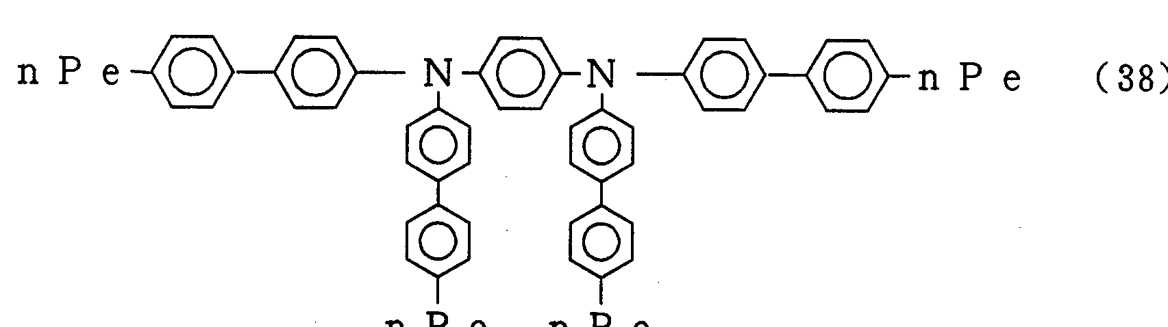
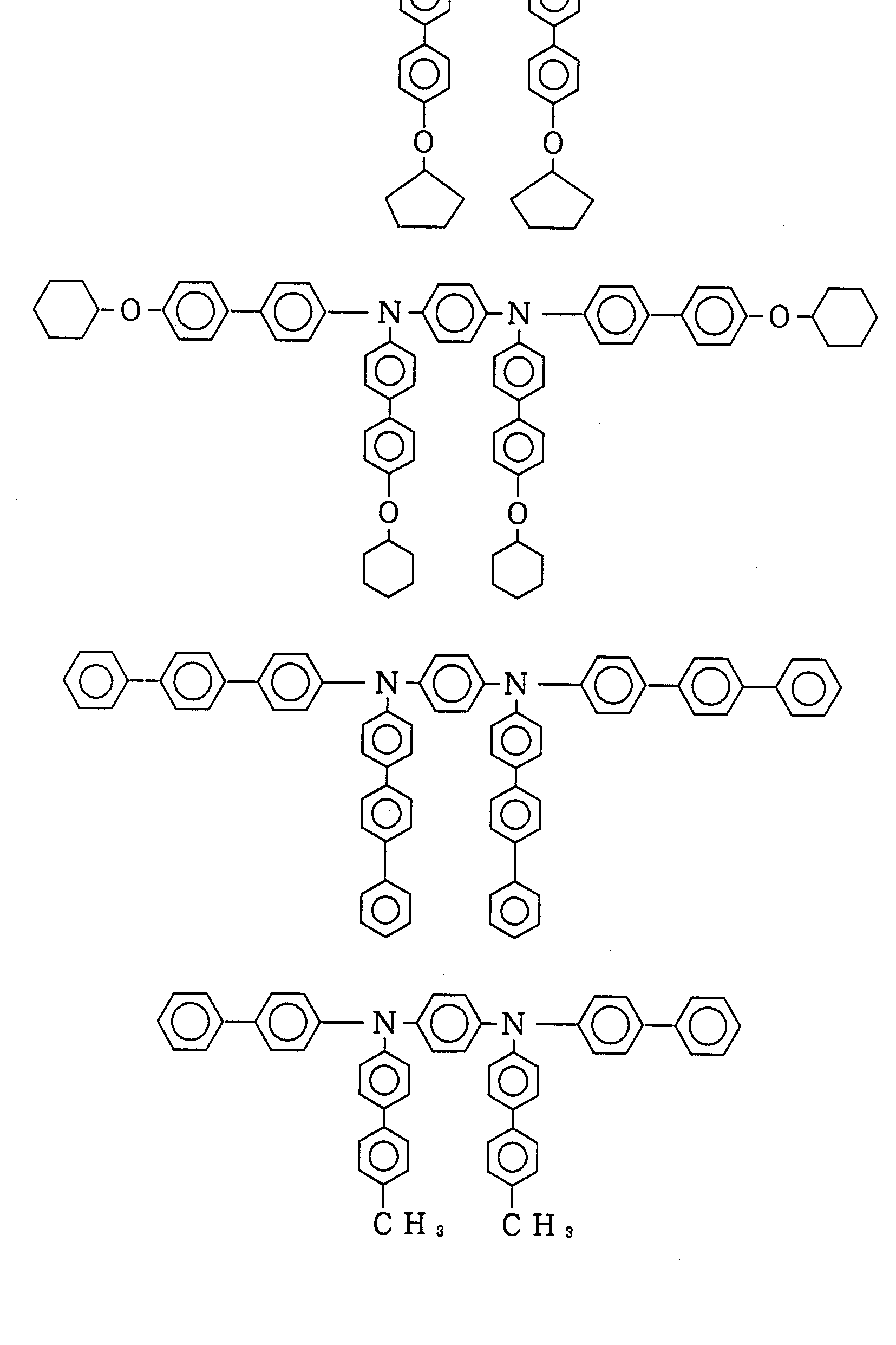
- a r 1, A r 2 , A r 3 and A r 4 are each an Ariru group having a carbon number of 6-2 0, they be the same or different from each other even if well, also Z, a r ', a r 2, a r 3 and a r 4 is Ku respectively Wakashi alkyl group of from 1 to 6 carbon may be substituted by alkoxy groups or Fuweniru group but, a r 1, a r 2 , a r 3 and a r 4 together with z of the central skeleton must have 6 or more benzene ring skeletons. ]
- An organic EL device containing at least a p-phenylenediamine derivative having at least 6 benzene ring skeletons represented by
- R 1G to R 17 each represent a hydrogen atom, an alkyl group or an alkoxy group having 1 to 6 carbon atoms, or a phenyl group, which may be the same or different;
- R 10 and R 11, R 11 and R 13, R 12 and R 13, R 14 and R 15, R 15 and R 17 and R '6 and R 17 are its Re respectively bonded to form a ring You may.
- R 10 and R 11, R 11 and R 13, R 12 and R 13, R 14 and R 15, R 15 and R 17 and R '6 and R 17 are its Re respectively bonded to form a ring You may.
- FIG. 1, FIG. 2, FIG. 3, and FIG. 4 are ⁇ -NMR spectrum diagrams of the compounds obtained in Production Example 4, Production Example 5, Production Example 6, and Production Example 7, respectively. .
- One of the arylene diamine derivatives used in the organic EL device of the present invention has a general formula (I)
- Z represents a p-phenylene group
- Ar S. Ar 3 and Ar 4 each represent an aryl group having 6 to 20 carbon atoms.
- the aryl group include a phenyl group, a naphthyl group, a biphenyl group, an anthranyl group, an acenaphthyl group, a phenanthryl group and a pyrenyl group.
- Z of p- phenylene group, ⁇ Li Lumpur group A r 1 ⁇ A r 4 are each an alkyl group of from 1 to 6 carbon atoms, such as methyl group, Echiru group, n- propyl group, Isopropyl group, cyclobutyl pill group, n-butyl group, isobutyl group, sec-butyl group, tert-butyl group, cyclobutyl group, n-pentyl group, cyclopentyl group, n-hexyl group, cyclohexyl A sil group or an alkoxy group having 1 to 6 carbon atoms, for example, methoxy group, ethoxy group, n-propoxy group, isopropoxy group, cyclopropoxy group, n-butoxy group, isobutoxy group, sec-butyl Toxic group, tert-butoxy group, cyclobutoxy group, n-pentoxy group, It may
- a r ', A r 2, A r 3 and A r 4 are each may be filed by the same, may be different, and A r 1, A r 2, A r 3 and A r 4 It must have at least 6 benzene ring skeletons including the Z of the central skeleton.
- R] to R 17 each represent a hydrogen atom or an alkyl group having 1 to 6 carbon atoms, for example, a methyl group, an ethyl group, an n-propyl group, an isopropyl group, a cycloalkyl group; Propyl group, n-butyl group, isobutyl group, sec-butyl group, tert-butyl group, cyclobutyl group, n-pentyl group, cyclopentyl group, n-hexyl group, cyclohexyl group, etc.
- alkoxy groups such as methoxy, ethoxy, n-propoxy, isopropoxy, cyclopropoxy, n-butoxy, isobutoxy, sec-butoxy, tert-butoxy, cyclobutoxy, Indicates n-pentoxy group, cyclopentoxy group, n-hexoxy group, cyclohexoxy group, etc., or fujyl group.
- R 1 to R a may be the same or different, and R 1 and R 2 , R 2 and R 4 , R 3 and R 4 , R 5 and R 6 , R 6 and R 8 , R 7 and R 8 , R 2 and R s , R 4 and R 9 , R 6 and R 9, R 8 and R 9 are each bonded to form a ring Is also good.
- R 1 () to R 17 may be the same or different, and R 10 and R ′ 1 , R 11 and R 13 , R 12 and R 13 , R 14 and R 15, R 15 and R 17 and R 16 and R 17 may be bonded to each other to form a ring.
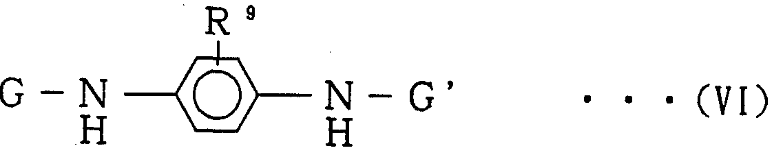
- X is a halogen atom (fluorine, chlorine, bromine, iodine), and R 1 and R 2 are the same as above. ]
- G and G ' are the same or different protecting groups, for example, acetyl group, benzyl group, trifluoroacetyl group, and -t-butoxycarbone.
- protecting groups for example, acetyl group, benzyl group, trifluoroacetyl group, and -t-butoxycarbone.
- Such group preferably an Asechiru group, R a is to be the same as above.
- halogenated aminoaryl compound represented by the general formula (V) is condensed with the halogenated arylaryl compound represented by the general formula (V). It can be manufactured by such as.
- halogenated aryl compounds represented by the general formula (V) include:
- aminoaryl halide compound represented by the general formula (IX) include:
- the condensation reaction may be performed in a solid phase without using a solvent, or may be performed in a solvent, but is preferably performed in a solvent.
- the solvent is preferably one having a high boiling point, for example, nitrobenzene, dimethylsulfoxide, dimethylformamide, sulfolane and the like are used. Of these, dimethyl sulfoxide is particularly preferred.
- the condensation reaction temperature is usually in the range of 100 to 400, preferably in the range of 150 to 250 ° C.
- the pressure for the condensation reaction is usually normal pressure, but the reaction may be performed under pressure if necessary.
- the condensation time depends on the type of raw material, catalyst, temperature, etc., and cannot be unconditionally determined, but is generally about 3 to 36 hours.
- R le to R 13 are the same as described above.
- halogenated aryl compounds represented by the general formula (XI) are as follows:
- Examples of the dihalogenated aryl compound represented by the general formula ⁇ ⁇ ) include:
- halogenated aminoaryl compound represented by the general formula (XIV) include H 2 , And the like.
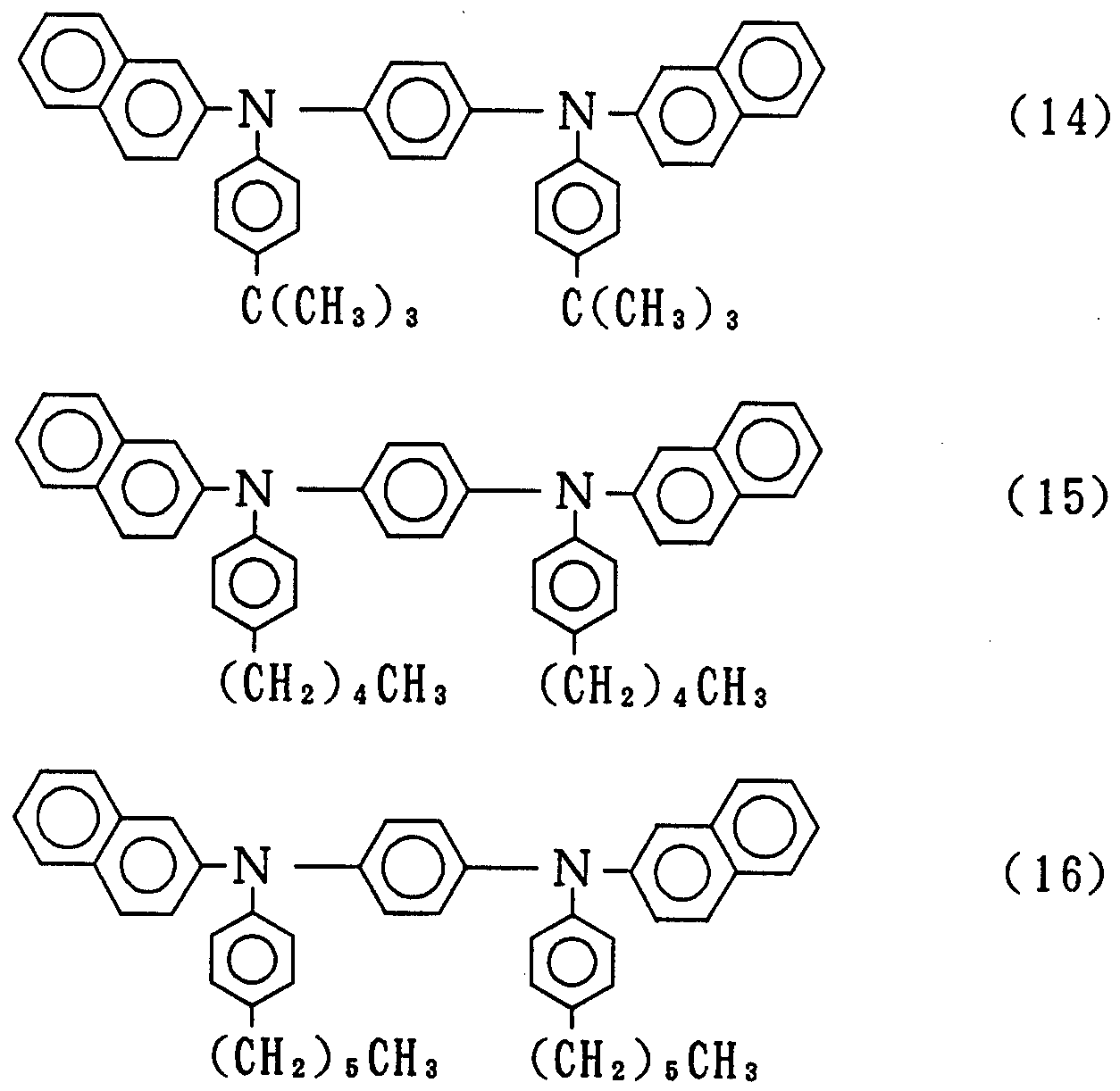
- a r], A r 2, A r 3 and A r 4 is intended preferably naphthyl or Bifuweniru group.
- the organic EL device of the present invention includes a p-phenylenediamine derivative represented by the general formula (I) [including a compound represented by the general formula (II)]. Or at least a 4,4'-biphenylenediamine derivative represented by the general formula (III).
- a p-phenylenediamine derivative represented by the general formula (I) [including a compound represented by the general formula (II)].
- one kind of the diamine derivative may be contained, or two or more kinds thereof may be contained in combination.
- the structure of the organic EL device is as follows: 1 Anode Organic light emitting layer Z cathode, 2 Positive hole transport layer / organic light emitting layer cathode, 3 Anode // organic light emitting layer Electron injection layer Z cathode, 4 Anode hole transport layer There are a Z organic light emitting layer, a Z electron injection layer, a cathode, and the like.
- the organic EL device of the present invention comprises a compound layer sandwiched between a pair of electrodes (anode and cathode) (the organic light emitting layer, In the device with the configuration of 2, the hole transport layer and the organic light emitting layer, At least one of the organic light-emitting layer and the electron injection layer in the device having the structure, and the hole transport layer, the organic light-emitting layer, and the electron injection layer in the device having the structure 4, are represented by the above-mentioned general formula (I).
- the organic light emitting layer In the device with the configuration of 2, the hole transport layer and the organic light emitting layer, At least one of the organic light-emitting layer and the electron injection layer in the device having the structure, and the hole transport layer, the organic light-emitting layer, and the electron injection layer in the device having the structure 4, are represented by the above-mentioned general formula (I).
- —Phenylenediamine derivative [Including the compound represented by the general formula (II).
- the substrate is not particularly limited, and those commonly used in conventional organic EL elements, for example, those made of glass, transparent plastic, quartz, or the like can be used.
- the hole transport layer containing the p-phenylenediamine derivative or the 4,4′-biphenylenediamine derivative is composed of only the p-phenylenediamine derivative or the 4,4′-biphenylenediamine derivative. Or a layer of a substance conventionally used as a hole transport layer material of an organic EL device with a p-phenylenediamine derivative or a 4,4'-biphenylenediamine derivative. And a multilayer structure. Furthermore, a single-layer structure including a layer made of a mixture of the P-phenylenediamine derivative or the 4,4′-biphenylenediamine derivative and a substance conventionally used as a hole transport layer material of an organic EL device. Alternatively, it may have a multilayer structure.
- the hole transporting layer containing the p-phenylenediamine derivative or the 4,4, -biphenylenediamine derivative is a p-phenylenediamine derivative.
- a 4,4'-biphenylenediamine derivative and, if necessary, other materials for the hole transport layer are formed by a vacuum deposition method, a casting method, a coating method, a spin coating method, or the like. be able to.
- a solution in which the p-phenylenediamine derivative or the 4,4'-biphenylenediamine derivative is dispersed in a transparent polymer such as polyforce—bone, polyurethane, polystyrene, polyarylate, or polyester is dispersed. It can also be formed by a casting method, a coating method, a spin coating method, or the like used, or a simultaneous vapor deposition with a transparent polymer.
- the organic light emitting layer containing the P-phenylenediamine derivative or the 4,4′-biphenylenediamine derivative is a single layer composed of only the p-phenylenediamine derivative or the 4,4′-biphenylenediamine derivative. It may have a structure, or a multilayer of a p-phenylenediamine derivative or a 4,4'-biphenylenediamine derivative and a layer of a substance conventionally used as a material for an organic light emitting layer of an organic EL device. It may have a structure.
- the organic EL device of the present invention is formed using the same material as that of the conventional organic EL device, except for the layer containing the p-f X-bendylenediamine derivative or the 4,4′-biphenylenediamine derivative. I can do this.
- a metal, an alloy, an electrically conductive compound or a mixture thereof having a large work function (4 eV or more) is preferably used as the material of the anode.
- Specific examples include metals such as Au, and dielectric transparent materials such as Cul, IT0, Sn02, and ⁇ 0.
- the material of the cathode metals, alloys, electrically conductive compounds or mixtures thereof having a low work function (4 eV or less) are preferably used.
- specific examples of the cathode material Na preparative potassium, lithium, mug Neshiumu Z copper mixtures, A 1 / A 1 2 0 3, etc.
- Lee indium is like et be.
- This cathode can be manufactured by forming a thin film of the above material by a method such as a vapor deposition method or a sputtering method. When light emitted from the organic light emitting layer is extracted from the cathode, the transmittance of the cathode is desirably greater than 10%.
- the sheet resistance of the cathode is preferably several hundred square ⁇ or less.
- the thickness of the cathode depends on the material, but is usually selected in the range of 10 nm to 10 nm, preferably in the range of 50 to 200 nm.
- the organic light emitting layer in the organic EL device of the present invention is formed from the p-phenylenediamine derivative or the 4,4′-biphenylenediamine derivative and another substance
- Rangeamine derivatives for example, a polycyclic fused aromatic compound or a fluorescent brightening agent such as a benzoxazole-based, benzothiazole-based, or benzimidabourne-based compound may be used.
- Compounds with good thin-film forming properties such as agents, metal chelated oxanoide compounds, and distyrylbenzene compounds, can be used.
- polycyclic fused aromatic compound examples include a condensed ring light-emitting substance containing an anthracene, naphthalene, phenanthrene, pyrene, chrysene, or perylene skeleton, and 8 to 20, preferably Include other condensed ring luminescent materials containing eight condensed rings.
- benzoxazole-based, benzothiazole-based, benzoimidazole-based fluorescent whitening agents include, for example, JP-A-59-91.
- metal chelated oxanoide compound for example, those disclosed in JP-A-63-956995 can be used.
- Typical examples are tris (8-quinolinol) aluminum, bis (8-quinolinol) magnesium, bis [benzo
- (f) -18-quinolinol) zinc bis (2-methyl-8-quinolinolate) aluminum oxide, tris (8-quinolinol) indium, tris (5— Methyl-8-quinolinol) aluminum, 8-quinolinollithium, tris (5-chloro-8-quinolinol) gallium, bis (5-crotinol.18-quinolinol) calcium, poly (Zinc (II) -bis (8-hydroxy-5-quinolinonyl) methane) and other 8—hydroxyquinoline-based metal complexes such as dilithium epinedridione.
- distyrylbenzene-based compound for example, those disclosed in European Patent No. 0 735 582 can be used. Typical examples are 1,4-bis (2-methylstyryl) benzene; 1,4-bis (3-methylstyryl) benzene;
- Rubirazine derivatives can also be used as a material for the organic light emitting layer.
- Typical examples are 2,5-bis (4-methylstyryl) pyrazine; 2,5-bis (4-ethylstyryl) pyrazine; 2,5-bis [2- (1-naphthyl) butyl] pyrazine; 2,5— Bis (4-methoxystyryl) pyrazine; 2,5-bis [2— (4-biphenyl) vinyl] pyrazine; 2,5—bis [2— (1-pyrenyl) vinyl] pyrazine;
- a dimethylidin derivative disclosed in European Patent No. 0 388 768 Japanese Unexamined Patent Application Publication No. 3-231970
- Typical examples are 1,41-phenylenedimethylidin; 4,4'-biphenylenedimethylidin; 2,5-xylylenedimethylidin; 2,6-naphthylenedimethylidin; 1,4 -Biphenylenedimethylidin; 1,4—p—Telephenylenedimethylidin; 9,10—Anthracenediyldimethylidin; 4,4′-1 (2,2—Gt-butylphenylvinyl) biphenyl 4,4 '-(2,2-diphenylvinyl) biphenyl and the like; and derivatives thereof.
- a coumarin derivative disclosed in Japanese Patent Application Laid-Open No. 2-196164 a perylene derivative disclosed in Japanese Patent Application Laid-Open No. 196885/1990, Naphthalene derivatives disclosed in US Pat. No. 5,578,893, and phthaloperinone derivatives disclosed in Japanese Patent Application Laid-Open Nos. 2-289676 and 2-88689
- a styrylamine derivative disclosed in JP-A-2-250292 can be used as a material for the organic light-emitting layer.
- organic light emitting layer materials are appropriately selected according to a desired light emitting color, performance, and the like.
- the organic light emitting layer in the organic EL device of the present invention As disclosed in US Pat. No. 4,769,292, a fluorescent material may be added.
- the base substance may be the p-phenylenediamine derivative or the 4,4′-biphenylenediamine derivative, or the p-phenylenediamine derivative or the p-phenylenediamine derivative.
- Organic light-emitting layer materials other than the 4,4′-biphenylenediamine derivative may be used. Further, it may be a mixture of the P-phenylenediamine derivative or the 4,4′-biphenylenediamine derivative with an organic light emitting layer material.
- the organic light emitting layer is formed by adding a fluorescent substance, the amount of the fluorescent substance added is preferably several mol% or less. Since the fluorescent substance emits light in response to recombination of electrons and holes, it plays a part in the light emitting function.
- the hole transporting layer used as necessary is such that the organic light emitting layer contains the p-phenylenediamine derivative or the 4,4′-biphenylenediamine derivative. Or a layer containing a p-phenylenediamine derivative or a 4,4′-biphenylenediamine derivative, or a layer containing the p-phenylenediamine derivative or the 4,4′-biphenylenediamine derivative May be included.
- the hole transport layer material other than the p_phenylene diamine derivative or the 4,4'-biphenylene diamine derivative various hole transport layer materials conventionally used as hole transport layer materials for organic EL devices can be used.
- the hole transport layer Is a single-layer structure composed of only a p-phenylenediamine derivative or a 4,4′-biphenylenediamine derivative, a p-phenylenediamine derivative or a 4,4′-biphenylenediamine derivative as described above.
- Organic EL devices have a multi-layered structure with a layer of a substance conventionally used as a hole transport layer material, or a p-phenylenediamine derivative or a 4,4'-biphenylenediamine derivative and a positive electrode of an organic EL device. It may have a single-layer structure or a multi-layer structure including a layer made of a mixture with a substance conventionally used as a hole transport layer material.
- a preferred layer structure is a single-layer structure composed only of the P-phenylenediamine derivative or 4,4′-biphenylenediamine derivative or the p-phenylenediamine derivative layer or the 4,4′-biphenyl diamine. It has a multi-layer structure of a rangeamine derivative layer and a layer of a porphyrin compound (disclosed in JP-A-63-295695) or a layer of an organic semiconductor oligomer.
- polyphenylene compounds include polyfin, 5,10,15,20—tetrafluoroethylene 21H—, 23H—borfin copper (II); 5,1 0, 15, 20 — Tetrafuline 21 H—, 23 H—porphyrin zinc (II); 5, 10, 15, 20 — Tetrax (perfluorophenyl) 121 H— , 23 H-porphin; silicon phthalocyanine oxide; aluminum phthalocyanine mouth lid; phthalocyanine (metal-free); dilithium phthalocyanine; copper tetramethyl phthalocyanine; copper phthalocyanine; chromium phthalocyanine; zinc phthalocyanine; Phthalocyanine; titanium lid Russian ninoxide; magnesium phthalocyanine: copper octamethyl phthalocyanine;
- organic semiconductor oligomer is preferably represented by the general formula (XV)
- R 18 , R 19 and R 2e each represent an alkyl group having 1 to 10 carbon atoms, an alkoxy group having 1 to 10 carbon atoms or a cyclohexyl group, and they may be the same or different.
- K, m and n are each an integer of 1 to 3, and their total amount is 5 or less.
- the compound represented by these is suitable.
- the electron injection layer (electron injection / transport layer) provided as needed only needs to have a function of transmitting electrons injected from the cathode to the organic light emitting layer.
- Preferred examples of the electron transfer compound include, for example,
- the electron injection layer is a layer having any of an electron injecting property, a transporting property, and a barrier property.
- Si-based and SiC A crystalline or non-crystalline material such as a CdS-based or CdS-based material can be used.
- the organic EL device of the present invention has a layer for improving the adhesion between the layers, in addition to the anode, the cathode, the organic light emitting layer, the hole transport layer and the electron injection layer provided as needed. Is also good.
- Specific examples of the material of such a layer for example, a layer for improving the adhesion between the organic light emitting layer and the cathode include tris (8-quinolinol) aluminum and tris (8-quinolinol). Quinolinol metal complex compounds such as indium.
- the above-described organic EL device of the present invention can be manufactured according to the configuration, for example, as follows.
- Anode Z organic light emitting layer (including p-phenylenediamine derivative or 4,4'-biphenylenediamine derivative) Production of organic EL device having Z-cathode structure First, a thin film made of a desired electrode material, for example, an anode material, is deposited and sputtered on a suitable substrate so as to have a thickness of 1 zm or less, preferably in the range of 10 to 200 nm. The anode is formed by such a method. Next, an organic light emitting layer is provided by forming a thin film of the p-phenylenediamine derivative or the 4,4′-biphenylenediamine derivative on the anode.
- a desired electrode material for example, an anode material
- This p-phenylenediamine derivative or 4,4′-biphenylenediamine derivative can be made into a thin film by a vacuum deposition method, a spin coating method, a casting method, or the like.
- the vacuum deposition method is preferred because it is easy to obtain and it is difficult to form pinholes.
- the deposition conditions are as follows: p-phenylenediamine derivative or 4,
- the biphenylenediamine derivative depends on the type of crystal structure and association structure of the target organic light-emitting layer.
- C vacuum degree of 1 0 - 6 ⁇ 1 0 _ 3 P a, the deposition rate 0. 0 1 ⁇ 5 0 nm / sec , substrate temperature one 5 0 tens 3 0 0 'C, thickness 5 Nm ⁇ 5 ⁇ m It is preferable to select appropriately within the range.
- a thin film made of a cathode material is deposited or sputtered on the organic light emitting layer so as to have a thickness of l zm or less, preferably in the range of 10 to 200 nm. It is formed by a method such as a ring to produce a cathode. As a result, a desired organic EL device is obtained.
- the production order may be reversed, and the cathode, the organic light-emitting layer, and the anode may be produced on the substrate in this order.
- Anode Z organic light emitting layer (P-phenylenediamine derivative or 4, 4'-Including the bi-diene diamine derivative) Production of Organic EL Element Having Z-Cathode Configuration 1-First, an anode is produced on a suitable substrate in the same manner as in the above (a). Next, an organic light emitting layer is provided by applying a solution containing a material for the hole transport layer, a material for the organic light emitting layer, a material for the electron injecting layer, and a binder (such as polyvinyl carbabour) on the anode.
- a binder such as polyvinyl carbabour
- the organic light emitting layer may have a multilayer structure by forming a thin film of a desired organic light emitting layer material on the layer formed as described above by a vacuum deposition method or the like.
- the organic light emitting layer material may be formed by co-evaporating the organic light emitting layer material together with the hole transport layer material and the electron injection layer material.
- an anode is formed on a suitable substrate in the same manner as in the above (a).
- a hole transport layer is provided by forming a thin film of the p-phenylenediamine derivative or the 4,4′-biphenylenediamine derivative on the anode.
- the formation of the hole transport layer can be performed in the same manner as the formation of the organic light emitting layer (including the P-phenylenediamine derivative or the 4,4′-biphenylenediamine derivative) in the above (a).
- an organic light emitting layer is provided on the hole transport layer using a desired organic light emitting layer material.
- the organic light-emitting layer is formed by vacuum evaporation, spin coating, and casting. It can be formed by reducing the thickness of the organic light emitting layer material by a method such as a vacuum method. However, a vacuum deposition method is preferable because a uniform film is easily obtained and pinholes are hardly generated.
- a thin film made of the cathode material is formed on the organic light emitting layer in the same manner as in the above (a), to produce a cathode. As a result, an intended organic EL device is obtained. In the production of this organic EL device, the production order can be reversed, and the cathode / organic light-emitting layer Z hole transport layer Z anode can be produced on the substrate in this order.
- Anode Z hole transport layer (including p-fuylene diamine derivative or 4,4'-biff X-bene diamine derivative) Z organic light emitting layer
- Electron injection layer Manufacture of organic EL device having cathode structure
- An anode, a hole transport layer (including a P-phenylenediamine derivative or a 4,4'-biphenylenediamine derivative) and an organic light-emitting layer are formed on a suitable substrate in the same manner as in the above (c). I do.
- a thin film made of an electron transfer compound is deposited on the organic light emitting layer so as to have a thickness of 1 ⁇ m or less, preferably in the range of 5 to 10 O nm by vapor deposition and sputtering.
- a thin film made of a cathode material is formed on the electron injection layer in the same manner as in the above (c) to form a cathode.
- the desired organic EL device is obtained.
- the production order can be reversed and the cathode Z electron injection layer / organic light emitting layer / hole transport layer Z anode can be formed on the base electrode in this order.
- the organic EL device of the present invention which can be manufactured in this manner, emits light by applying a direct current voltage of 5 to 40 V with the anode having ten polarities and the cathode having one polarity. Even if voltage is applied with the opposite polarity, current will not flow. No light emission occurs. When an AC voltage is applied, light emission occurs only when the anode has ten polarities and the cathode has one polarity. When an AC voltage is applied, the waveform of the AC may be arbitrary.
- the organic EL device of the present invention is a device having at least one compound layer having a single-layer structure or a multi-layer structure containing at least an organic light-emitting layer and containing a p-phenylenediamine derivative having six or more benzene ring skeletons.
- At least one of the compound layers having a single-layer structure or a multilayer structure including at least a light-emitting layer contains a 4,4′-biphenylenediamine derivative having five biphenyl groups, and has a luminescence lifetime of at least one. Is improved and the durability is extremely good.
- N, N, diphenyl 1,4-phenylenediamine [manufactured by Kanto Chemical Co., Ltd.] 3.42 g (13.2 mimol), 4-dithiophene [manufactured by Nard Institute] 9.3 5 g (33.4 millimol), carbonic anhydride rim 5.22 g (37.8 millimol) and 1 g (16 mimol) of copper powder were added to 300 milliliter eggplant. The mixture was placed in a flask, suspended in 300 milliliters of dimethyl sulfoxide (DMS0), and reacted at 180 ° C for 5 hours.
- DMS0 dimethyl sulfoxide
- the inorganic substance was filtered, the mother liquor was extracted with methylene chloride, dried over anhydrous sodium sulfate, and the solvent was distilled off using an evaporator.
- the obtained compound was purified using a column carrying Kogel C-200 (manufactured by Hiroshima Wako Co., Ltd.) using toluene as a developing solvent, to obtain 2.53 g of a pale yellow powder. .
- N, ⁇ '-G (2-naphthyl) 1-1,4-phenylenediamine manufactured by Kanto Chemical Co., Ltd.
- 6.84 g (49.6 millimoles) of anhydrous potassium carbonate and 1 g (16 millimoles) of copper powder were added to 300
- the mixture was placed in a milliliter eggplant flask, suspended in 300 milliliters of DMS 0, and reacted at 180 for 5 hours.
- the inorganic substance was filtered, and the mother liquor was washed with methylene chloride.
- N, N, zzy (2-naphthyl) 1,4-phenylenediamine [manufactured by Kanto Chemical Co., Ltd.] 2.13 g (5.92 mimol), 4-dodiphenyl [ner Laboratories] 4.70 g (16.8 mimol), calcium anhydride (3.19 g, 23.3 mimol) and copper powder 1 g (16 mimol)
- the mixture was placed in a 300-milliliter eggplant flask, suspended in 300-milliliter DMS0, and reacted at 180 ° C. for 5 hours. After the inorganic substance was filtered, the mother liquor was extracted with methylene chloride, dried over anhydrous sodium sulfate, and the solvent was distilled off using an evaporator.
- the obtained compound was purified using toluene as a developing solvent using a column supporting Picogel C1200 (manufactured by Hiroshima Wako), and a pale yellow powder was obtained.
- the pale yellow powder was identified as ⁇ , ⁇ , N ′, N′-tetrakis (4-biphenyl) -11,41-phenylenediamine [compound (27)].
- the yield was 20% and the melting point was 310 ° C.
- N, N'-Diacetyl-4,4'-I-benzidine (manufactured by Tokyo Chemical Industry Co., Ltd.) 5.03 g (18.8 mimol), 4-iododiphenyl 12.3 g (43.8 mimol), anhydrous Place 11 g (80 mimol) of potassium carbonate and lg (16 mimol) of copper powder in a 300-milliliter eggplant flask and suspend them in a DMS ⁇ 200-milliliter. Turbid, 180. After reacting with C for 5 hours, the inorganic substance was filtered, the filtrate was extracted with methylene chloride, dried over anhydrous sodium sulfate, and then the solvent was distilled off using an evaporator.
- This intermediate 1.02 g (2.09 mimol), 4-iododiphenyl 1.54 g (5.50 mimol), anhydrous carbon dioxide 1.9 g (14.4 mi) 1 mol (16 mol) of copper powder was placed in a 300-milliliter three-necked flask, and suspended in 200 ml of DMS O2O. The reaction was carried out for 5 hours with TC. The inorganic substance was filtered, the mother liquor was extracted with methylene chloride, dried over anhydrous sodium sulfate, and the solvent was distilled off using an evaporator. Was purified using a column supporting Kogel Co., Ltd. [200] [manufactured by Hiroshima Wako Co., Ltd.] using toluene as a developing solvent, to obtain 0.50 g of a pale yellow powder.
- a transparent support substrate was obtained by forming an ITO electrode with a thickness of 100 nm on a glass substrate of 25 mm ⁇ 75 mm ⁇ 1 mm. This was ultrasonically cleaned with pill alcohol at the outlet.
- This transparent support substrate was fixed to the substrate holder of a vacuum evaporation system [manufactured by Nippon Vacuum Engineering Co., Ltd.], and tris was attached to a molybdenum resistance heating boat.
- MT DATA (3-Methylphenylphenylamino) Triphenylamine (MT DATA) Add 20 mg of the compound and place it in another molybdenum resistance heating boat.
- DPVB i 4,4′-bis (2,2-diphenylvinyl) biphenyl
- Vacuum Chiyanba one in the 1 X 1 0 -. 4 P a was evacuated to, MTD A TA 0. heating the entering ports 1-0 at 311,111 sec rate of 1 ⁇ Ding 0 eight TA the I TO electrodes A 60 nm film was formed thereon. Thereafter, the boat containing the compound (1) was heated, and the compound (1) was deposited at a deposition rate of 0.1 to 0.3 nmZ seconds to form a hole transport layer having a thickness of 20 nm. Then, this On the hole transport layer, DPVB i was deposited as a shipping layer by 4 O nm from the other three layers. The deposition rate was between 0.1 and 0.2 nm.
- a cathode was fabricated by depositing silver at a deposition rate of 0.1 nmZ seconds at a time of .8 nmZ seconds.
- Example 1 was repeated except that the compound (1) obtained in Production Example 1 was replaced by the compound (2) obtained in Production Example 2 as the hole transporting material. Thus, an element was manufactured.
- Example 1 was repeated in the same manner as in Example 1 except that the compound (1) obtained in Production Example 3 was replaced with the compound (3) obtained in Production Example 3 as the hole transporting material. Thus, an element was manufactured.
- Example 5 In the same manner as in Example 1 except that the compound (27) obtained in Production Example 4 was used in place of the compound (1) obtained in Production Example 1 as the hole transporting material. Thus, an element was produced.
- Example 5 In the same manner as in Example 1 except that the compound (27) obtained in Production Example 4 was used in place of the compound (1) obtained in Production Example 1 as the hole transporting material. Thus, an element was produced.
- Example 1 was repeated except that the compound (28) obtained in Production Example 5 was used in place of the compound (1) obtained in Production Example 1 as the hole transporting material. Thus, an element was manufactured.
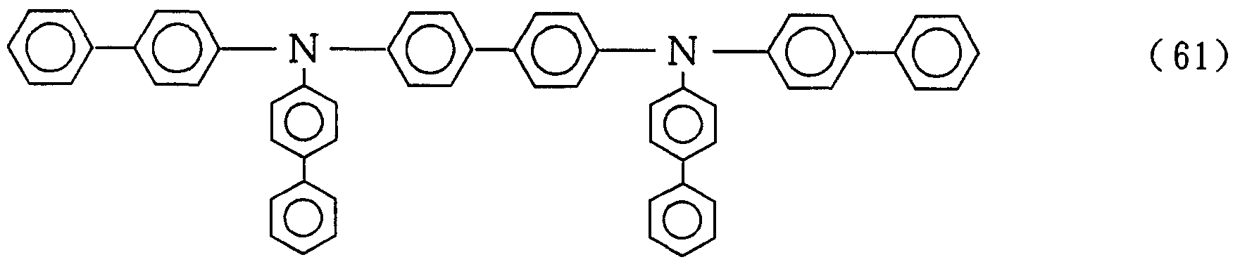
- Example 1 was repeated except that the compound (61) obtained in Production Example 6 was used in place of the compound (1) obtained in Production Example 1 as the hole transporting material. Thus, an element was manufactured.
- Example 1 instead of the compound (1) obtained in Production Example 1 as a hole transport material, N, N'-diphenyl N, N'-bis ((3-methylphenyl) 1-1,1 ' -A device was prepared in the same manner as in Example 1 except that biphenyl 2,4 'diamin (TPD) was used.
- TPD biphenyl 2,4 'diamin
- Example 1 except that the compound (1) obtained in Production Example 1 was replaced by N, N, ⁇ ', N'-tetraphenylene ⁇ -fuylenediamine as the hole transporting material in Example 1, A device was manufactured in the same manner as in Example 1.
- Example 1 instead of the compound (1) obtained in Production Example 1 as a hole transporting material, ⁇ , —, ⁇ ′, N′—tetrakis (4-biphenyl) 1 m-phenylenediamine Example 1 and An element was produced in the same manner.
- Example 1 the compound (1) obtained in Production Example 1 was replaced with N, N, ⁇ ', N'-tetrakis (4-biphenyl) -1,3,3,1-dimethyl A device was fabricated in the same manner as in Example 1, except that 4,4'-benzidine was used.
- Table 1 shows the emission lifetimes of the devices of Examples 1 to 7 and Comparative Examples 1 to 4.
- the emission lifetime is the time required for each element to be driven at a constant current and starting with an initial luminance of 10 O cdZ m 2 until the luminance is reduced by half to 50 cd / m 2 .
- the devices of Examples 1 to 7 have remarkably improved luminescence lifetime as compared with TPD (Comparative Example 1) which is a hole transporting material having the longest luminescence lifetime among known techniques.
- N, N, ⁇ ′, ⁇ ′-tetraphenyl- ⁇ -phenylenediamine of Comparative Example 2 is a well-known hole transporting material, but it has high crystallinity because there are only five benzene rings in the molecule. Dielectric breakdown occurred during the life measurement. In contrast, all of the compounds of Examples 1 to 7 do not crystallize because they have 6 or more benzene rings in the molecule, and can maintain a uniform thin film for a long time.
- Comparative Example 3 also has no problem in thin-film property because it has six or more benzene rings in the molecule, but it emits light. The life was remarkably short.
- N, N, N ', N'-tetrakis (4-biphenyl) -3,3'-dimethyl-1,4'-benzidine of Comparative Example 4 also has six or more benzene rings in the molecule, and thus has a thin film property. There was no problem, but the emission lifetime was extremely short. Table 1
- the organic EL element of the present invention contains a p-phenylenediamine derivative or a 4,4′-biphenylenediamine derivative as an element component, and has an improved light emission lifetime and improved durability. It has features such as excellence.
- the arylenediamine derivative of the present invention can significantly improve the light emission lifetime of an organic EL device.
Landscapes
- Chemical & Material Sciences (AREA)
- Organic Chemistry (AREA)
- Engineering & Computer Science (AREA)
- Materials Engineering (AREA)
- Physics & Mathematics (AREA)
- Spectroscopy & Molecular Physics (AREA)
- Electroluminescent Light Sources (AREA)
- Organic Low-Molecular-Weight Compounds And Preparation Thereof (AREA)
- Luminescent Compositions (AREA)
- Low-Molecular Organic Synthesis Reactions Using Catalysts (AREA)
Description














Claims


Priority Applications (4)
| Application Number | Priority Date | Filing Date | Title |
|---|---|---|---|
| DE69432054T DE69432054T2 (de) | 1993-09-29 | 1994-09-28 | Organische elektrolumineszenzelemente und arylendiaminderivate |
| US08/615,281 US5837166A (en) | 1993-09-29 | 1994-09-28 | Organic electroluminescence device and arylenediamine derivative |
| JP51020995A JP3295088B2 (ja) | 1993-09-29 | 1994-09-28 | 有機エレクトロルミネッセンス素子 |
| EP94927780A EP0721935B1 (en) | 1993-09-29 | 1994-09-28 | Organic electroluminescent element and arylenediamine derivative |
Applications Claiming Priority (2)
| Application Number | Priority Date | Filing Date | Title |
|---|---|---|---|
| JP24302493 | 1993-09-29 | ||
| JP5/243024 | 1993-09-29 |
Publications (1)
| Publication Number | Publication Date |
|---|---|
| WO1995009147A1 true WO1995009147A1 (en) | 1995-04-06 |
Family
ID=17097741
Family Applications (1)
| Application Number | Title | Priority Date | Filing Date |
|---|---|---|---|
| PCT/JP1994/001585 Ceased WO1995009147A1 (en) | 1993-09-29 | 1994-09-28 | Organic electroluminescent element and arylenediamine derivative |
Country Status (5)
| Country | Link |
|---|---|
| US (1) | US5837166A (ja) |
| EP (2) | EP0721935B1 (ja) |
| JP (2) | JP3295088B2 (ja) |
| DE (2) | DE69432686T2 (ja) |
| WO (1) | WO1995009147A1 (ja) |
Cited By (212)
| Publication number | Priority date | Publication date | Assignee | Title |
|---|---|---|---|---|
| US5728801A (en) * | 1996-08-13 | 1998-03-17 | The Dow Chemical Company | Poly (arylamines) and films thereof |
| JPH1088119A (ja) * | 1996-09-11 | 1998-04-07 | Sharp Corp | 有機電界発光素子 |
| US5929194A (en) * | 1996-02-23 | 1999-07-27 | The Dow Chemical Company | Crosslinkable or chain extendable polyarylpolyamines and films thereof |
| US5948552A (en) * | 1996-08-27 | 1999-09-07 | Hewlett-Packard Company | Heat-resistant organic electroluminescent device |
| JP2000133453A (ja) * | 1998-10-22 | 2000-05-12 | Idemitsu Kosan Co Ltd | 有機エレクトロルミネッセンス素子およびその製造方法 |
| JP2000164358A (ja) * | 1998-11-24 | 2000-06-16 | Matsushita Electric Ind Co Ltd | 有機薄膜el素子およびその駆動方法 |
| WO1997033193A3 (en) * | 1996-02-23 | 2002-09-26 | Dow Chemical Co | Cross-linkable or chain extendable polyarylpolyamines and films thereof |
| JPWO2002076922A1 (ja) * | 2001-03-16 | 2004-07-15 | 出光興産株式会社 | 芳香族アミノ化合物の製造方法 |
| JPWO2002094965A1 (ja) * | 2001-05-24 | 2004-09-09 | 出光興産株式会社 | 有機エレクトロルミネッセンス素子 |
| JP2007269738A (ja) * | 2006-03-31 | 2007-10-18 | Tdk Corp | 有機el素子用化合物及び有機el素子 |
| JP2009135511A (ja) * | 1994-02-08 | 2009-06-18 | Tdk Corp | 有機el素子 |
| DE102009005746A1 (de) | 2009-01-23 | 2010-07-29 | Merck Patent Gmbh | Materialien für organische Elektrolumineszenzvorrichtungen |
| DE102009009277A1 (de) | 2009-02-17 | 2010-08-19 | Merck Patent Gmbh | Organische elektronische Vorrichtung |
| WO2010108579A1 (de) | 2009-03-23 | 2010-09-30 | Merck Patent Gmbh | Organische elektrolumineszenzvorrichtung |
| DE102009017064A1 (de) | 2009-04-09 | 2010-10-14 | Merck Patent Gmbh | Organische Elektrolumineszenzvorrichtung |
| WO2010149259A2 (en) | 2009-06-22 | 2010-12-29 | Merck Patent Gmbh | Conducting formulation |
| WO2011012212A1 (de) | 2009-07-27 | 2011-02-03 | Merck Patent Gmbh | Neue materialien für organische elektrolumineszenzvorrichtungen |
| DE102009041289A1 (de) | 2009-09-16 | 2011-03-17 | Merck Patent Gmbh | Organische Elektrolumineszenzvorrichtung |
| DE102009042680A1 (de) | 2009-09-23 | 2011-03-24 | Merck Patent Gmbh | Organische Elektrolumineszenzvorrichtung |
| WO2011035836A1 (de) | 2009-09-23 | 2011-03-31 | Merck Patent Gmbh | Materialien für elektronische vorrichtungen |
| DE102009053191A1 (de) | 2009-11-06 | 2011-05-12 | Merck Patent Gmbh | Materialien für elektronische Vorrichtungen |
| DE102009052428A1 (de) | 2009-11-10 | 2011-05-12 | Merck Patent Gmbh | Verbindung für elektronische Vorrichtungen |
| WO2011076325A1 (en) | 2009-12-23 | 2011-06-30 | Merck Patent Gmbh | Compositions comprising polymeric binders |
| WO2011076324A1 (en) | 2009-12-23 | 2011-06-30 | Merck Patent Gmbh | Compositions comprising organic semiconducting compounds |
| DE102010010481A1 (de) | 2010-03-06 | 2011-09-08 | Merck Patent Gmbh | Organische Elektrolumineszenzvorrichtung |
| DE102010010631A1 (de) | 2010-03-09 | 2011-09-15 | Merck Patent Gmbh | Materialien für elektronische Vorrichtungen |
| WO2011128035A1 (en) | 2010-04-12 | 2011-10-20 | Merck Patent Gmbh | Composition and method for preparation of organic electronic devices |
| WO2011128034A1 (en) | 2010-04-12 | 2011-10-20 | Merck Patent Gmbh | Composition having improved performance |
| DE102010020044A1 (de) | 2010-05-11 | 2011-11-17 | Merck Patent Gmbh | Organische Elektrolumineszenzvorrichtung |
| WO2011147523A1 (en) | 2010-05-27 | 2011-12-01 | Merck Patent Gmbh | Formulation and method for preparation of organic electronic devices |
| DE102010048074A1 (de) | 2010-10-09 | 2012-04-12 | Merck Patent Gmbh | Materialien für elektronische Vorrichtungen |
| WO2012048780A1 (de) | 2010-10-15 | 2012-04-19 | Merck Patent Gmbh | Verbindungen für elektronische vorrichtungen |
| WO2012095143A1 (de) | 2011-01-13 | 2012-07-19 | Merck Patent Gmbh | Verbindungen für organische elektrolumineszenzvorrichtungen |
| WO2012149992A1 (de) | 2011-05-04 | 2012-11-08 | Merck Patent Gmbh | Vorrichtung zur aufbewahrung von frischwaren |
| DE102011104745A1 (de) | 2011-06-17 | 2012-12-20 | Merck Patent Gmbh | Materialien für organische Elektrolumineszenzvorrichtungen |
| DE102012016192A1 (de) | 2011-08-19 | 2013-02-21 | Merck Patent Gmbh | Neue Materialien für organische Elektrolumineszenzvorrichtungen |
| WO2013026515A1 (de) | 2011-08-22 | 2013-02-28 | Merck Patent Gmbh | Organische elektrolumineszenzvorrichtung |
| WO2013050101A1 (de) | 2011-10-06 | 2013-04-11 | Merck Patent Gmbh | Organische elektrolumineszenzvorrichtung |
| DE102012022880A1 (de) | 2011-12-22 | 2013-06-27 | Merck Patent Gmbh | Elektronische Vorrichtungen enthaltend organische Schichten |
| JP2013531658A (ja) * | 2010-06-17 | 2013-08-08 | イー・アイ・デュポン・ドウ・ヌムール・アンド・カンパニー | 電気活性材料 |
| WO2013135352A1 (de) | 2012-03-15 | 2013-09-19 | Merck Patent Gmbh | Elektronische vorrichtungen |
| WO2014044344A1 (de) | 2012-09-18 | 2014-03-27 | Merck Patent Gmbh | Materialien für elektronische vorrichtungen |
| WO2014067614A1 (de) | 2012-10-31 | 2014-05-08 | Merck Patent Gmbh | Elektronische vorrichtung |
| WO2014082705A1 (de) | 2012-11-30 | 2014-06-05 | Merck Patent Gmbh | Elektronische vorrichtung |
| KR20140072802A (ko) * | 2012-12-05 | 2014-06-13 | 유니버셜 디스플레이 코포레이션 | 트위스트 아릴 기를 갖는 정공 수송 물질 |
| WO2014106522A1 (de) | 2013-01-03 | 2014-07-10 | Merck Patent Gmbh | Materialien für elektronische vorrichtungen |
| WO2014106524A2 (de) | 2013-01-03 | 2014-07-10 | Merck Patent Gmbh | Materialien für elektronische vorrichtungen |
| WO2014106523A1 (de) | 2013-01-03 | 2014-07-10 | Merck Patent Gmbh | Elektronische vorrichtung |
| WO2015082037A1 (en) | 2013-12-06 | 2015-06-11 | Merck Patent Gmbh | Compositions containing a polymeric binder which comprises acrylic and/or methacrylic acid ester units |
| WO2015082046A2 (de) | 2013-12-06 | 2015-06-11 | Merck Patent Gmbh | Substituierte oxepine |
| WO2015165563A1 (de) | 2014-04-30 | 2015-11-05 | Merck Patent Gmbh | Materialien für elektronische vorrichtungen |
| JP2015201279A (ja) * | 2014-04-04 | 2015-11-12 | セイコーエプソン株式会社 | 発光素子、発光装置、表示装置および電子機器 |
| JP2015201496A (ja) * | 2014-04-04 | 2015-11-12 | セイコーエプソン株式会社 | 発光素子、発光装置、表示装置および電子機器 |
| WO2015192941A1 (de) | 2014-06-18 | 2015-12-23 | Merck Patent Gmbh | Zusammensetzungen für elektronische vorrichtungen |
| WO2016119992A1 (en) | 2015-01-30 | 2016-08-04 | Merck Patent Gmbh | Materials for electronic devices |
| WO2016120007A1 (en) | 2015-01-30 | 2016-08-04 | Merck Patent Gmbh | Formulations with a low particle content |
| WO2016124304A1 (de) | 2015-02-03 | 2016-08-11 | Merck Patent Gmbh | Metallkomplexe |
| WO2017008883A1 (en) | 2015-07-15 | 2017-01-19 | Merck Patent Gmbh | Composition comprising organic semiconducting compounds |
| WO2017012694A1 (en) | 2015-07-23 | 2017-01-26 | Merck Patent Gmbh | Phenyl derivatives substituted with at least two electron acceptors and at least two electron donors for use in organic electronic devices |
| WO2017028940A1 (en) | 2015-08-14 | 2017-02-23 | Merck Patent Gmbh | Phenoxazine derivatives for organic electroluminescent devices |
| WO2017036573A1 (en) | 2015-08-28 | 2017-03-09 | Merck Patent Gmbh | Compounds for electronic devices |
| WO2017133829A1 (de) | 2016-02-05 | 2017-08-10 | Merck Patent Gmbh | Materialien für elektronische vorrichtungen |
| JP2017204492A (ja) * | 2016-05-09 | 2017-11-16 | 保土谷化学工業株式会社 | 有機エレクトロルミネッセンス素子 |
| WO2018007421A1 (en) | 2016-07-08 | 2018-01-11 | Merck Patent Gmbh | Materials for organic electroluminescent devices |
| WO2018069167A1 (de) | 2016-10-10 | 2018-04-19 | Merck Patent Gmbh | Elektronische vorrichtung |
| WO2018083053A1 (de) | 2016-11-02 | 2018-05-11 | Merck Patent Gmbh | Materialien für elektronische vorrichtungen |
| WO2018095839A1 (de) | 2016-11-22 | 2018-05-31 | Merck Patent Gmbh | Verbrückte triarylamine für elektronische vorrichtungen |
| WO2018095888A1 (en) | 2016-11-25 | 2018-05-31 | Merck Patent Gmbh | Bisbenzofuran-fused 2,8-diaminoindeno[1,2-b]fluorene derivatives and related compounds as materials for organic electroluminescent devices (oled) |
| WO2018095940A1 (en) | 2016-11-25 | 2018-05-31 | Merck Patent Gmbh | Bisbenzofuran-fused indeno[1,2-b]fluorene derivatives and related compounds as materials for organic electroluminescent devices (oled) |
| WO2018134392A1 (en) | 2017-01-23 | 2018-07-26 | Merck Patent Gmbh | Materials for organic electroluminescent devices |
| WO2018141706A1 (de) | 2017-02-02 | 2018-08-09 | Merck Patent Gmbh | Materialien für elektronische vorrichtungen |
| WO2018158232A1 (en) | 2017-03-01 | 2018-09-07 | Merck Patent Gmbh | Organic electroluminescent device |
| WO2018157981A1 (de) | 2017-03-02 | 2018-09-07 | Merck Patent Gmbh | Materialien für organische elektronische vorrichtungen |
| EP3378857A1 (de) | 2012-11-12 | 2018-09-26 | Merck Patent GmbH | Materialien für elektronische vorrichtungen |
| WO2018189134A1 (de) | 2017-04-13 | 2018-10-18 | Merck Patent Gmbh | Zusammensetzung für organische elektronische vorrichtungen |
| WO2018197447A1 (de) | 2017-04-25 | 2018-11-01 | Merck Patent Gmbh | Verbindungen für elektronische vorrichtungen |
| WO2018234346A1 (en) | 2017-06-23 | 2018-12-27 | Merck Patent Gmbh | Materials for organic electroluminescent devices |
| WO2019002198A1 (en) | 2017-06-26 | 2019-01-03 | Merck Patent Gmbh | HOMOGENEOUS MIXTURES |
| WO2019002190A1 (en) | 2017-06-28 | 2019-01-03 | Merck Patent Gmbh | MATERIALS FOR ELECTRONIC DEVICES |
| WO2019007823A1 (en) | 2017-07-03 | 2019-01-10 | Merck Patent Gmbh | LOW-PHENOL IMPURITY FORMULATIONS |
| WO2019007866A1 (de) | 2017-07-05 | 2019-01-10 | Merck Patent Gmbh | Zusammensetzung für organische elektronische vorrichtungen |
| WO2019007867A1 (de) | 2017-07-05 | 2019-01-10 | Merck Patent Gmbh | Zusammensetzung für organische elektronische vorrichtungen |
| WO2019020538A1 (de) | 2017-07-25 | 2019-01-31 | Merck Patent Gmbh | Metallkomplexe |
| WO2019020654A1 (en) | 2017-07-28 | 2019-01-31 | Merck Patent Gmbh | SPIROBIFLUORENE DERIVATIVES FOR USE IN ELECTRONIC DEVICES |
| WO2019048443A1 (de) | 2017-09-08 | 2019-03-14 | Merck Patent Gmbh | Materialien für elektronische vorrichtungen |
| WO2019076789A1 (en) | 2017-10-17 | 2019-04-25 | Merck Patent Gmbh | MATERIALS FOR ORGANIC ELECTROLUMINESCENT DEVICES |
| WO2019096717A2 (de) | 2017-11-14 | 2019-05-23 | Merck Patent Gmbh | Zusammensetzung für organische elektronische vorrichtungen |
| WO2019101833A1 (en) | 2017-11-24 | 2019-05-31 | Merck Patent Gmbh | Materials for organic electroluminescent devices |
| WO2019101719A1 (de) | 2017-11-23 | 2019-05-31 | Merck Patent Gmbh | Materialien für elektronische vorrichtungen |
| WO2019101835A1 (en) | 2017-11-24 | 2019-05-31 | Merck Patent Gmbh | Materials for organic electroluminescent devices |
| WO2019115423A1 (de) | 2017-12-13 | 2019-06-20 | Merck Patent Gmbh | Metallkomplexe |
| WO2019115577A1 (en) | 2017-12-15 | 2019-06-20 | Merck Patent Gmbh | Substituted aromatic amines for use in organic electroluminescent devices |
| WO2019158453A1 (de) | 2018-02-13 | 2019-08-22 | Merck Patent Gmbh | Metallkomplexe |
| WO2019170572A1 (en) | 2018-03-06 | 2019-09-12 | Merck Patent Gmbh | Materials for organic electroluminescent devices |
| WO2019170578A1 (en) | 2018-03-06 | 2019-09-12 | Merck Patent Gmbh | Materials for organic electroluminescent devices |
| WO2019175149A1 (en) | 2018-03-16 | 2019-09-19 | Merck Patent Gmbh | Materials for organic electroluminescent devices |
| EP3553050A1 (en) | 2018-04-10 | 2019-10-16 | Samsung SDI Co., Ltd. | Composition and organic optoelectronic device and display device |
| US10483329B2 (en) | 2016-12-28 | 2019-11-19 | Shanghai Tianma AM-OLED Co., Ltd. | Hole transporting material, hole transporting layer, OLED display panel electronic device comprising the same |
| EP3575296A1 (en) | 2018-05-28 | 2019-12-04 | Samsung SDI Co., Ltd. | Triazine compound, composition and organic optoelectronic device and display device |
| WO2019229011A1 (de) | 2018-05-30 | 2019-12-05 | Merck Patent Gmbh | Zusammensetzung für organische elektronische vorrichtungen |
| WO2020043646A1 (en) | 2018-08-28 | 2020-03-05 | Merck Patent Gmbh | Materials for organic electroluminescent devices |
| WO2020043657A1 (en) | 2018-08-28 | 2020-03-05 | Merck Patent Gmbh | Materials for organic electroluminescent devices |
| WO2020043640A1 (en) | 2018-08-28 | 2020-03-05 | Merck Patent Gmbh | Materials for organic electroluminescent devices |
| WO2020053150A1 (en) | 2018-09-12 | 2020-03-19 | Merck Patent Gmbh | Materials for organic electroluminescent devices |
| EP3647393A1 (de) | 2013-07-30 | 2020-05-06 | Merck Patent GmbH | Materialien für elektronische vorrichtungen |
| WO2020089138A1 (en) | 2018-10-31 | 2020-05-07 | Merck Patent Gmbh | Materials for organic electroluminescent devices |
| EP3660012A1 (en) | 2018-11-28 | 2020-06-03 | Samsung SDI Co., Ltd. | Compound for organic optoelectronic device and organic optoelectronic device and display device |
| WO2020130381A1 (ko) | 2018-12-21 | 2020-06-25 | 삼성에스디아이 주식회사 | 유기 광전자 소자용 화합물, 유기 광전자 소자용 조성물, 유기 광전자 소자 및 표시 장치 |
| WO2020145508A1 (ko) | 2019-01-10 | 2020-07-16 | 삼성에스디아이 주식회사 | 유기 광전자 소자용 화합물, 유기 광전자 소자 및 표시 장치 |
| WO2020165064A1 (de) | 2019-02-11 | 2020-08-20 | Merck Patent Gmbh | Mononukleare iridiumkomplexe mit drei ortho-metallierten bidentaten liganden und optischer orientierungsanisotropie |
| WO2020169241A1 (de) | 2019-02-18 | 2020-08-27 | Merck Patent Gmbh | Zusammensetzung für organische elektronische vorrichtungen |
| WO2020178230A1 (en) | 2019-03-04 | 2020-09-10 | Merck Patent Gmbh | Ligands for nano-sized materials |
| EP3712229A1 (de) | 2013-07-30 | 2020-09-23 | Merck Patent GmbH | Materialien für elektronische vorrichtungen |
| WO2020208051A1 (en) | 2019-04-11 | 2020-10-15 | Merck Patent Gmbh | Materials for organic electroluminescent devices |
| WO2020263029A1 (ko) | 2019-06-28 | 2020-12-30 | 삼성에스디아이 주식회사 | 유기 광전자 소자용 화합물, 유기 광전자 소자용 조성물, 유기 광전자 소자 및 표시 장치 |
| WO2021052921A1 (de) | 2019-09-19 | 2021-03-25 | Merck Patent Gmbh | Mischung von zwei hostmaterialien und organische elektrolumineszierende vorrichtung damit |
| WO2021089450A1 (en) | 2019-11-04 | 2021-05-14 | Merck Patent Gmbh | Materials for organic electroluminescent devices |
| WO2021089447A1 (de) | 2019-11-04 | 2021-05-14 | Merck Patent Gmbh | Organische elektrolumineszierende vorrichtung |
| WO2021094269A1 (en) | 2019-11-12 | 2021-05-20 | Merck Patent Gmbh | Materials for organic electroluminescent devices |
| WO2021110720A1 (de) | 2019-12-04 | 2021-06-10 | Merck Patent Gmbh | Metallkomplexe |
| WO2021110741A1 (en) | 2019-12-04 | 2021-06-10 | Merck Patent Gmbh | Materials for organic electroluminescent devices |
| WO2021180614A1 (de) | 2020-03-11 | 2021-09-16 | Merck Patent Gmbh | Organische elektrolumineszierende vorrichtung |
| WO2021180950A1 (en) | 2020-03-13 | 2021-09-16 | Merck Patent Gmbh | Materials for organic electroluminescent devices |
| WO2021180625A1 (de) | 2020-03-11 | 2021-09-16 | Merck Patent Gmbh | Organische elektrolumineszierende vorrichtung |
| WO2021191058A1 (en) | 2020-03-23 | 2021-09-30 | Merck Patent Gmbh | Materials for organic electroluminescent devices |
| WO2021239772A1 (de) | 2020-05-29 | 2021-12-02 | Merck Patent Gmbh | Organische elektrolumineszierende vorrichtung |
| US11217756B2 (en) | 2018-05-04 | 2022-01-04 | Samsung Sdi Co., Ltd. | Compound for organic optoelectronic device, composition for organic optoelectronic device and organic optoelectronic device and display device |
| US11223019B2 (en) | 2017-06-22 | 2022-01-11 | Samsung Sdi Co., Ltd. | Compound for organic optoelectronic device, composition for organic optoelectronic device and organic optoelectronic device and display device |
| WO2022017998A1 (en) | 2020-07-22 | 2022-01-27 | Merck Patent Gmbh | Materials for organic electroluminescent devices |
| WO2022017997A1 (en) | 2020-07-22 | 2022-01-27 | Merck Patent Gmbh | Materials for organic electroluminescent devices |
| WO2022055169A1 (ko) | 2020-09-09 | 2022-03-17 | 삼성에스디아이 주식회사 | 유기 광전자 소자용 화합물, 유기 광전자 소자용 조성물, 유기 광전자 소자 및 표시 장치 |
| WO2022069380A1 (de) | 2020-09-29 | 2022-04-07 | Merck Patent Gmbh | Mononukleare tripodale hexadentate iridium komplexe zur verwendung in oleds |
| US11329232B2 (en) * | 2018-04-23 | 2022-05-10 | Samsung Display Co., Ltd. | Arylamine-based compound including thermally decomposable groups and organic light-emitting device including the same |
| WO2022112541A1 (en) | 2020-11-30 | 2022-06-02 | Merck Patent Gmbh | Materials for organic electroluminescent devices |
| WO2022146011A1 (ko) | 2020-12-30 | 2022-07-07 | 삼성에스디아이 주식회사 | 유기 광전자 소자용 화합물, 유기 광전자 소자용 조성물, 유기 광전자 소자 및 표시 장치 |
| US11453659B2 (en) | 2019-06-28 | 2022-09-27 | Samsung Sdi Co., Ltd. | Compound for organic optoelectronic device, composition for organic optoelectronic device, organic optoelectronic device and display device |
| US11459316B2 (en) | 2019-05-30 | 2022-10-04 | Samsung Sdi Co., Ltd. | Compound for organic optoelectronic device, composition for organic optoelectronic device, organic optoelectronic device, and display device |
| WO2022211594A1 (ko) | 2021-04-01 | 2022-10-06 | 삼성에스디아이 주식회사 | 유기 광전자 소자용 조성물, 유기 광전자 소자 및 표시 장치 |
| WO2022214566A1 (en) | 2021-04-09 | 2022-10-13 | Merck Patent Gmbh | Materials for organic electroluminescent devices |
| WO2022214506A1 (en) | 2021-04-09 | 2022-10-13 | Merck Patent Gmbh | Materials for organic electroluminescent devices |
| WO2022214507A1 (en) | 2021-04-09 | 2022-10-13 | Merck Patent Gmbh | Materials for organic electroluminescent devices |
| EP4079742A1 (de) | 2021-04-14 | 2022-10-26 | Merck Patent GmbH | Metallkomplexe |
| WO2023282602A1 (ko) | 2021-07-06 | 2023-01-12 | 삼성에스디아이 주식회사 | 유기 광전자 소자용 화합물, 유기 광전자 소자 및 표시 장치 |
| WO2023282617A2 (ko) | 2021-07-06 | 2023-01-12 | 삼성에스디아이 주식회사 | 유기 광전자 소자용 조성물, 유기 광전자 소자 및 표시 장치 |
| WO2023282603A1 (ko) | 2021-07-06 | 2023-01-12 | 삼성에스디아이 주식회사 | 유기 광전자 소자용 조성물, 유기 광전자 소자 및 표시 장치 |
| US11569455B2 (en) | 2019-06-13 | 2023-01-31 | Samsung Sdi Co., Ltd. | Compound for organic optoelectronic device, organic optoelectronic device, and display device |
| WO2023036976A1 (en) | 2021-09-13 | 2023-03-16 | Merck Patent Gmbh | Materials for organic electroluminescent devices |
| WO2023052314A1 (de) | 2021-09-28 | 2023-04-06 | Merck Patent Gmbh | Materialien für elektronische vorrichtungen |
| WO2023052275A1 (de) | 2021-09-28 | 2023-04-06 | Merck Patent Gmbh | Materialien für elektronische vorrichtungen |
| WO2023052313A1 (de) | 2021-09-28 | 2023-04-06 | Merck Patent Gmbh | Materialien für elektronische vorrichtungen |
| WO2023052272A1 (de) | 2021-09-28 | 2023-04-06 | Merck Patent Gmbh | Materialien für elektronische vorrichtungen |
| WO2023094412A1 (de) | 2021-11-25 | 2023-06-01 | Merck Patent Gmbh | Materialien für elektronische vorrichtungen |
| WO2023117837A1 (de) | 2021-12-21 | 2023-06-29 | Merck Patent Gmbh | Verfahren zur herstellung von deuterierten organischen verbindungen |
| WO2023128513A1 (ko) | 2021-12-30 | 2023-07-06 | 삼성에스디아이 주식회사 | 유기 광전자 소자용 화합물, 유기 광전자 소자용 조성물, 유기 광전자 소자 및 표시 장치 |
| WO2023152346A1 (de) | 2022-02-14 | 2023-08-17 | Merck Patent Gmbh | Materialien für elektronische vorrichtungen |
| US11800794B2 (en) | 2017-06-22 | 2023-10-24 | Samsung Sdi Co., Ltd. | Compound for organic optoelectronic device, composition for organic optoelectronic device and organic optoelectronic device and display device |
| WO2023208899A1 (en) | 2022-04-28 | 2023-11-02 | Merck Patent Gmbh | Materials for organic electroluminescent devices |
| WO2023222559A1 (de) | 2022-05-18 | 2023-11-23 | Merck Patent Gmbh | Verfahren zur herstellung von deuterierten organischen verbindungen |
| WO2023247662A1 (de) | 2022-06-24 | 2023-12-28 | Merck Patent Gmbh | Zusammensetzung für organische elektronische vorrichtungen |
| WO2023247663A1 (de) | 2022-06-24 | 2023-12-28 | Merck Patent Gmbh | Zusammensetzung für organische elektronische vorrichtungen |
| US11871659B2 (en) | 2019-02-15 | 2024-01-09 | Samsung Sdi Co., Ltd. | Composition for optoelectronic device and organic optoelectronic device and display device |
| WO2024013004A1 (de) | 2022-07-11 | 2024-01-18 | Merck Patent Gmbh | Materialien für elektronische vorrichtungen |
| WO2024033282A1 (en) | 2022-08-09 | 2024-02-15 | Merck Patent Gmbh | Materials for organic electroluminescent devices |
| US11932661B2 (en) | 2020-03-23 | 2024-03-19 | Samsung Sdi Co., Ltd. | Composition for organic optoelectronic device, organic optoelectronic device, and display device |
| WO2024063628A1 (ko) | 2022-09-23 | 2024-03-28 | 삼성에스디아이 주식회사 | 유기 광전자 소자용 화합물, 유기 광전자 소자용 조성물, 유기 광전자 소자 및 표시 장치 |
| WO2024094670A1 (en) | 2022-11-04 | 2024-05-10 | Merck Patent Gmbh | Materials for organic electroluminescent devices |
| WO2024105066A1 (en) | 2022-11-17 | 2024-05-23 | Merck Patent Gmbh | Materials for organic electroluminescent devices |
| US12010913B2 (en) | 2019-10-02 | 2024-06-11 | Samsung Sdi Co., Ltd. | Compound for organic optoelectronic device, organic optoelectronic device and display device |
| WO2024133366A1 (en) | 2022-12-23 | 2024-06-27 | Merck Patent Gmbh | Electronic device |
| WO2024132993A1 (de) | 2022-12-19 | 2024-06-27 | Merck Patent Gmbh | Materialien für elektronische vorrichtungen |
| WO2024132892A1 (en) | 2022-12-19 | 2024-06-27 | Merck Patent Gmbh | Materials for organic electroluminescent devices |
| WO2024133048A1 (en) | 2022-12-20 | 2024-06-27 | Merck Patent Gmbh | Method for preparing deuterated aromatic compounds |
| US12029112B2 (en) | 2019-02-15 | 2024-07-02 | Samsung Sdi Co., Ltd. | Composition for optoelectronic device and organic optoelectronic device and display device |
| US12030894B2 (en) | 2020-09-04 | 2024-07-09 | Samsung Sdi Co., Ltd. | Composition for organic optoelectronic device, organic optoelectronic device and display device |
| US12048239B2 (en) | 2020-04-20 | 2024-07-23 | Samsung Sdi Co., Ltd. | Composition for organic optoelectronic device, organic optoelectronic device and display device |
| US12069947B2 (en) | 2020-06-30 | 2024-08-20 | Samsung Sdi Co., Ltd. | Composition for optoelectronic device and organic optoelectronic device and display device |
| WO2024170605A1 (en) | 2023-02-17 | 2024-08-22 | Merck Patent Gmbh | Materials for organic electroluminescent devices |
| WO2024170609A1 (en) | 2023-02-17 | 2024-08-22 | Merck Patent Gmbh | Materials for organic electroluminescent devices |
| WO2024177457A1 (ko) | 2023-02-23 | 2024-08-29 | 삼성에스디아이 주식회사 | 유기 광전자 소자용 화합물, 유기 광전자 소자용 조성물, 유기 광전자 소자 및 표시 장치 |
| WO2024177455A1 (ko) | 2023-02-23 | 2024-08-29 | 삼성에스디아이 주식회사 | 유기 광전자 소자용 화합물, 유기 광전자 소자용 조성물, 유기 광전자 소자 및 표시 장치 |
| US12096688B2 (en) | 2020-07-03 | 2024-09-17 | Samsung Sdi Co., Ltd. | Composition for organic optoelectronic device, organic optoelectronic device and display device |
| US12096684B2 (en) | 2020-08-10 | 2024-09-17 | Samsung Sdi Co., Ltd. | Composition for organic optoelectronic device, organic optoelectronic device and display device |
| US12108657B2 (en) | 2019-09-30 | 2024-10-01 | Samsung Sdi Co., Ltd. | Compound for organic optoelectronic device, composition for organic optoelectronic device, organic optoelectronic device and display device |
| WO2024218109A1 (de) | 2023-04-20 | 2024-10-24 | Merck Patent Gmbh | Materialien für elektronische vorrichtungen |
| US12133460B2 (en) | 2019-10-23 | 2024-10-29 | Samsung Sdi Co., Ltd. | Compound for organic optoelectronic device, composition for organic optoelectronic device, organic optoelectronic device and display device |
| US12144249B2 (en) | 2020-07-17 | 2024-11-12 | Samsung Sdi Co., Ltd. | Compound for organic optoelectronic device, composition for organic optoelectronic device, organic optoelectronic device and display device |
| WO2024240725A1 (de) | 2023-05-25 | 2024-11-28 | Merck Patent Gmbh | Tris[1,2,4]triazolo[1,5-a:1',5'-c:1'',5''-e][1,3,5]triazin-derivate zur verwendung in organischen elektrolumineszenzvorrichtungen |
| WO2024242339A1 (ko) | 2023-05-23 | 2024-11-28 | 삼성에스디아이 주식회사 | 유기 광전자 소자 및 표시 장치 |
| US12178117B2 (en) | 2020-06-10 | 2024-12-24 | Samsung Electronics Co., Ltd. | Composition and organic light-emitting device including the same |
| WO2025012253A1 (en) | 2023-07-12 | 2025-01-16 | Merck Patent Gmbh | Materials for electronic devices |
| WO2025021855A1 (de) | 2023-07-27 | 2025-01-30 | Merck Patent Gmbh | Materialien für organische lichtemittierende vorrichtungen und organische sensoren |
| US12219869B2 (en) | 2020-11-03 | 2025-02-04 | Samsung Sdi Co., Ltd. | Composition for organic optoelectronic device, organic optoelectronic device, and display device |
| WO2025045843A1 (de) | 2023-08-30 | 2025-03-06 | Merck Patent Gmbh | Materialien für organische lichtemittierende vorrichtungen |
| WO2025045851A1 (de) | 2023-08-30 | 2025-03-06 | Merck Patent Gmbh | Materialien für organische lichtemittierende vorrichtungen |
| WO2025045842A1 (de) | 2023-08-30 | 2025-03-06 | Merck Patent Gmbh | Materialien für organische lichtemittierende vorrichtungen |
| US12274160B2 (en) | 2020-06-02 | 2025-04-08 | Samsung Sdi Co., Ltd. | Composition for organic optoelectronic device and organic optoelectronic device and display device |
| WO2025083015A1 (en) | 2023-10-19 | 2025-04-24 | Merck Patent Gmbh | Materials for organic electroluminescent devices |
| US12295254B2 (en) | 2020-04-07 | 2025-05-06 | Samsung Sdi Co., Ltd. | Compound for organic optoelectronic device, composition for organic optoelectronic device, organic optoelectronic device, and display device |
| US12302751B2 (en) | 2018-06-12 | 2025-05-13 | Samsung Sdi Co., Ltd. | Composition for organic optoelectronic device, organic optoelectronic device, and display device |
| WO2025119821A1 (en) | 2023-12-05 | 2025-06-12 | Merck Patent Gmbh | Material composition for organic electroluminescent devices |
| WO2025132551A1 (de) | 2023-12-22 | 2025-06-26 | Merck Patent Gmbh | Materialien für elektronische vorrichtungen |
| WO2025132547A1 (en) | 2023-12-21 | 2025-06-26 | Merck Patent Gmbh | Mechanochemical method for deuterating organic compounds |
| US12410200B2 (en) | 2020-06-02 | 2025-09-09 | Samsung Sdi Co., Ltd. | Composition for organic optoelectronic device, organic optoelectronic device, and display device |
| WO2025196145A1 (en) | 2024-03-22 | 2025-09-25 | Merck Patent Gmbh | Materials for organic light emitting devices |
| US12433152B2 (en) | 2020-01-30 | 2025-09-30 | Samsung Sdi Co., Ltd. | Compound for organic optoelectronic device, composition for organic optoelectronic device, organic optoelectronic device and display device |
| WO2025210013A1 (de) | 2024-04-04 | 2025-10-09 | Merck Patent Gmbh | Verbindungen für elektronische vorrichtungen, insbesondere verbindungen für oleds |
| US12473256B2 (en) | 2020-06-09 | 2025-11-18 | Samsung Sdi Co., Ltd. | Composition for organic optoelectronic device and organic optoelectronic device and display device |
| US12492216B2 (en) | 2021-02-25 | 2025-12-09 | Samsung Sdi Co., Ltd. | Compound for organic optoelectronic device, composition for organic optoelectronic device, organic optoelectronic device and display device |
| US12501829B2 (en) | 2020-11-04 | 2025-12-16 | Samsung Sdi Co., Ltd. | Compound for organic optoelectronic device, composition for organic optoelectronic device, organic optoelectronic device, and display device |
| WO2026017611A1 (en) | 2024-07-15 | 2026-01-22 | Merck Patent Gmbh | Organic light emitting device |
| US12557546B2 (en) | 2019-11-14 | 2026-02-17 | Samsung Sdi Co., Ltd. | Compound for organic optoelectronic device, composition for organic optoelectronic device, organic optoelectronic device and display device |
| US12590101B2 (en) | 2019-10-29 | 2026-03-31 | Samsung Sdi Co., Ltd. | Compound for organic optoelectronic device, composition for organic optoelectronic device and organic optoelectronic device and display device |
Families Citing this family (81)
| Publication number | Priority date | Publication date | Assignee | Title |
|---|---|---|---|---|
| JPH11199864A (ja) * | 1997-10-10 | 1999-07-27 | Koto Gijutsu Kenkyuin Kenkyu Kumiai | 電気発光素子の製造方法 |
| JP4545243B2 (ja) * | 1997-12-16 | 2010-09-15 | チッソ株式会社 | ジアミノナフタレン誘導体、及びそれを用いた有機電界発光素子 |
| WO2000014174A1 (en) * | 1998-09-09 | 2000-03-16 | Idemitsu Kosan Co., Ltd. | Organic electroluminescence device and phenylenediamine derivative |
| EP1666561A1 (en) | 1998-12-28 | 2006-06-07 | Idemitsu Kosan Company Limited | Organic electroluminescent element |
| US6576340B1 (en) * | 1999-11-12 | 2003-06-10 | E. I. Du Pont De Nemours And Company | Acid dyeable polyester compositions |
| WO2001056091A2 (de) * | 2000-01-28 | 2001-08-02 | Siemens Aktiengesellschaft | Ladungstransportmaterial mit erhöhter glasübergangstemperatur und verwendung des materials |
| US20020037427A1 (en) * | 2000-03-31 | 2002-03-28 | Toshiki Taguchi | Organic light emitting device material, amine compound, heterocyclic compound and organic light emitting devices using the same |
| GB0031634D0 (en) * | 2000-12-23 | 2001-02-07 | Johnson Matthey Plc | Organic materials |
| CN100431193C (zh) * | 2001-06-06 | 2008-11-05 | 出光兴产株式会社 | 有机电致发光器件 |
| JP2004262761A (ja) * | 2003-01-16 | 2004-09-24 | Idemitsu Kosan Co Ltd | 芳香族アミン誘導体及びそれを用いた有機エレクトロルミネッセンス素子 |
| KR100696470B1 (ko) * | 2004-06-15 | 2007-03-19 | 삼성에스디아이 주식회사 | 유기 전계 발광 소자 |
| KR100700013B1 (ko) * | 2004-11-26 | 2007-03-26 | 삼성에스디아이 주식회사 | 유기전계발광소자 및 그의 제조 방법 |
| JP2007186461A (ja) * | 2006-01-13 | 2007-07-26 | Idemitsu Kosan Co Ltd | 芳香族アミン誘導体及びそれを用いた有機エレクトロルミネッセンス素子 |
| JP5209325B2 (ja) | 2006-01-25 | 2013-06-12 | 保土谷化学工業株式会社 | p−ターフェニル化合物混合物及び該化合物混合物を用いた電子写真用感光体 |
| US20080299474A1 (en) * | 2007-05-31 | 2008-12-04 | Xerox Corporation | High quality substituted aryl diamine and a photoreceptor |
| WO2011015265A2 (en) | 2009-08-04 | 2011-02-10 | Merck Patent Gmbh | Electronic devices comprising multi cyclic hydrocarbons |
| US9666806B2 (en) | 2009-09-16 | 2017-05-30 | Merck Patent Gmbh | Formulations for the production of electronic devices |
| WO2011076323A1 (en) | 2009-12-22 | 2011-06-30 | Merck Patent Gmbh | Formulations comprising phase-separated functional materials |
| WO2011076314A1 (en) | 2009-12-22 | 2011-06-30 | Merck Patent Gmbh | Electroluminescent formulations |
| EP2517537B1 (en) | 2009-12-22 | 2019-04-03 | Merck Patent GmbH | Electroluminescent functional surfactants |
| EP2544765A1 (en) | 2010-03-11 | 2013-01-16 | Merck Patent GmbH | Fibers in therapy and cosmetics |
| KR101757016B1 (ko) | 2010-03-11 | 2017-07-11 | 메르크 파텐트 게엠베하 | 방사성 섬유 |
| US10190043B2 (en) | 2010-05-27 | 2019-01-29 | Merck Patent Gmbh | Compositions comprising quantum dots |
| CN103026525B (zh) | 2010-07-26 | 2016-11-09 | 默克专利有限公司 | 在器件中的纳米晶体 |
| JP2013539584A (ja) | 2010-07-26 | 2013-10-24 | メルク パテント ゲーエムベーハー | 量子ドットおよびホスト |
| WO2012110178A1 (en) | 2011-02-14 | 2012-08-23 | Merck Patent Gmbh | Device and method for treatment of cells and cell tissue |
| US9923152B2 (en) | 2011-03-24 | 2018-03-20 | Merck Patent Gmbh | Organic ionic functional materials |
| JP6223961B2 (ja) | 2011-05-12 | 2017-11-01 | メルク パテント ゲーエムベーハー | 有機イオン性機能材料、組成物および電子素子 |
| WO2012163464A1 (en) | 2011-06-01 | 2012-12-06 | Merck Patent Gmbh | Hybrid ambipolar tfts |
| EP2737553A1 (en) | 2011-07-25 | 2014-06-04 | Merck Patent GmbH | Copolymers with functionalized side chains |
| DE102011117422A1 (de) | 2011-10-28 | 2013-05-02 | Merck Patent Gmbh | Hyperverzweigte Polymere, Verfahren zu deren Herstellung sowie deren Verwendung in elektronischen Vorrichtungen |
| JP6567519B2 (ja) | 2013-07-29 | 2019-08-28 | メルク、パテント、ゲゼルシャフト、ミット、ベシュレンクテル、ハフツングMerck Patent GmbH | エレクトロルミネッセンス素子 |
| WO2015014427A1 (de) | 2013-07-29 | 2015-02-05 | Merck Patent Gmbh | Elektrooptische vorrichtung und deren verwendung |
| EP2924753B1 (en) * | 2014-03-25 | 2017-04-19 | Novaled GmbH | Polychromatic light emitting devices and versatile hole transporting matrix for them |
| KR101733151B1 (ko) * | 2014-08-21 | 2017-05-08 | 삼성디스플레이 주식회사 | 유기 발광 소자 및 이를 포함하는 유기 발광 표시 장치 |
| EP3189551B1 (de) | 2014-09-05 | 2021-01-27 | Merck Patent GmbH | Formulierungen und verfahren zur herstellung einer organischen elektrolumineszenzvorrichtung |
| TWI569492B (zh) * | 2014-12-22 | 2017-02-01 | 昱鐳光電科技股份有限公司 | 有機發光元件 |
| WO2016107663A1 (de) | 2014-12-30 | 2016-07-07 | Merck Patent Gmbh | Formulierungen und elektronische vorrichtungen |
| JP6800879B2 (ja) | 2015-03-30 | 2020-12-16 | メルク パテント ゲーエムベーハー | シロキサン溶媒を含む有機機能性材料の調合物 |
| CN111477766B (zh) | 2015-06-12 | 2023-04-07 | 默克专利有限公司 | 作为用于oled制剂的溶剂的含有非芳族环的酯 |
| WO2017036572A1 (en) | 2015-08-28 | 2017-03-09 | Merck Patent Gmbh | Formulation of an organic functional material comprising an epoxy group containing solvent |
| US11005042B2 (en) | 2015-12-10 | 2021-05-11 | Merck Patent Gmbh | Formulations containing ketones comprising non-aromatic cycles |
| EP4084109A1 (en) | 2015-12-15 | 2022-11-02 | Merck Patent GmbH | Esters containing aromatic groups as solvents for organic electronic formulations |
| KR20180095028A (ko) | 2015-12-16 | 2018-08-24 | 메르크 파텐트 게엠베하 | 둘 이상의 상이한 용매의 혼합물을 함유하는 제형 |
| JP7438661B2 (ja) | 2015-12-16 | 2024-02-27 | メルク パテント ゲーエムベーハー | 固体溶媒を含む調合物 |
| KR102776731B1 (ko) | 2016-02-17 | 2025-03-05 | 메르크 파텐트 게엠베하 | 유기 기능성 재료의 제형 |
| DE102016003104A1 (de) | 2016-03-15 | 2017-09-21 | Merck Patent Gmbh | Behälter umfassend eine Formulierung enthaltend mindestens einen organischen Halbleiter |
| JP2019523997A (ja) | 2016-06-16 | 2019-08-29 | メルク パテント ゲーエムベーハー | 有機機能材料の調合物 |
| CN109312183A (zh) | 2016-06-17 | 2019-02-05 | 默克专利有限公司 | 有机功能材料的制剂 |
| TW201815998A (zh) | 2016-06-28 | 2018-05-01 | 德商麥克專利有限公司 | 有機功能材料之調配物 |
| WO2018024719A1 (en) | 2016-08-04 | 2018-02-08 | Merck Patent Gmbh | Formulation of an organic functional material |
| KR102451842B1 (ko) | 2016-10-31 | 2022-10-07 | 메르크 파텐트 게엠베하 | 유기 기능성 재료의 제형 |
| WO2018077662A1 (en) | 2016-10-31 | 2018-05-03 | Merck Patent Gmbh | Formulation of an organic functional material |
| WO2018104202A1 (en) | 2016-12-06 | 2018-06-14 | Merck Patent Gmbh | Preparation process for an electronic device |
| WO2018108760A1 (en) | 2016-12-13 | 2018-06-21 | Merck Patent Gmbh | Formulation of an organic functional material |
| KR102504432B1 (ko) | 2016-12-22 | 2023-02-27 | 메르크 파텐트 게엠베하 | 적어도 2종의 유기-기능성 화합물을 포함하는 혼합물 |
| CN106810456B (zh) * | 2016-12-28 | 2019-12-10 | 上海天马有机发光显示技术有限公司 | 一种空穴传输材料、包含其的oled显示面板和电子设备 |
| CN107275362B (zh) | 2016-12-28 | 2020-10-09 | 上海天马有机发光显示技术有限公司 | 一种oled显示面板及包含其的电子设备 |
| CN106748815B (zh) * | 2016-12-28 | 2019-07-05 | 上海天马有机发光显示技术有限公司 | 一种空穴传输材料、包含其的oled显示面板和电子设备 |
| TWI763772B (zh) | 2017-01-30 | 2022-05-11 | 德商麥克專利有限公司 | 電子裝置之有機元件的形成方法 |
| TWI791481B (zh) | 2017-01-30 | 2023-02-11 | 德商麥克專利有限公司 | 形成有機電致發光(el)元件之方法 |
| CN110446611B (zh) | 2017-03-31 | 2021-05-25 | 默克专利有限公司 | 用于有机发光二极管(oled)的印刷方法 |
| KR102632027B1 (ko) | 2017-04-10 | 2024-01-31 | 메르크 파텐트 게엠베하 | 유기 기능성 재료의 제형 |
| JP7330898B2 (ja) | 2017-05-03 | 2023-08-22 | メルク パテント ゲーエムベーハー | 有機機能材料の調合物 |
| WO2019016184A1 (en) | 2017-07-18 | 2019-01-24 | Merck Patent Gmbh | FORMULATION OF AN ORGANIC FUNCTIONAL MATERIAL |
| CN111418081B (zh) | 2017-12-15 | 2024-09-13 | 默克专利有限公司 | 有机功能材料的制剂 |
| KR102710151B1 (ko) | 2018-02-26 | 2024-09-25 | 메르크 파텐트 게엠베하 | 유기 기능성 재료의 포뮬레이션 |
| WO2019238782A1 (en) | 2018-06-15 | 2019-12-19 | Merck Patent Gmbh | Formulation of an organic functional material |
| JP2022502829A (ja) | 2018-09-24 | 2022-01-11 | メルク パテント ゲーエムベーハー | 粒状材料を製造するための方法 |
| EP3878022A1 (en) | 2018-11-06 | 2021-09-15 | Merck Patent GmbH | Method for forming an organic element of an electronic device |
| CN110669040A (zh) | 2019-09-26 | 2020-01-10 | 上海天马有机发光显示技术有限公司 | 化合物、显示面板和显示装置 |
| WO2021213917A1 (en) | 2020-04-21 | 2021-10-28 | Merck Patent Gmbh | Emulsions comprising organic functional materials |
| CN115867426A (zh) | 2020-06-23 | 2023-03-28 | 默克专利有限公司 | 生产混合物的方法 |
| KR20230114756A (ko) | 2020-12-08 | 2023-08-01 | 메르크 파텐트 게엠베하 | 잉크 시스템 및 잉크젯 인쇄를 위한 방법 |
| EP4340969A1 (de) | 2021-05-21 | 2024-03-27 | Merck Patent GmbH | Verfahren zur kontinuierlichen aufreinigung von mindestens einem funktionalen material und vorrichtung zur kontinuierlichen aufreinigung von mindestens einem funktionalen material |
| JP2024528219A (ja) | 2021-08-02 | 2024-07-26 | メルク パテント ゲーエムベーハー | インクを組み合わせることによる印刷方法 |
| KR20240052050A (ko) | 2021-08-31 | 2024-04-22 | 메르크 파텐트 게엠베하 | 조성물 |
| TW202349760A (zh) | 2021-10-05 | 2023-12-16 | 德商麥克專利有限公司 | 電子裝置之有機元件的形成方法 |
| TW202411366A (zh) | 2022-06-07 | 2024-03-16 | 德商麥克專利有限公司 | 藉由組合油墨來印刷電子裝置功能層之方法 |
| TW202440819A (zh) | 2022-12-16 | 2024-10-16 | 德商麥克專利有限公司 | 有機功能性材料之調配物 |
| WO2025032039A1 (en) | 2023-08-07 | 2025-02-13 | Merck Patent Gmbh | Process for the preparation of an electronic device |
Citations (7)
| Publication number | Priority date | Publication date | Assignee | Title |
|---|---|---|---|---|
| JPH03173095A (ja) * | 1989-11-30 | 1991-07-26 | Pioneer Electron Corp | 電界発光素子 |
| JPH04161480A (ja) * | 1990-10-25 | 1992-06-04 | Mitsubishi Kasei Corp | 有機電界発光素子 |
| JPH04233195A (ja) * | 1990-07-26 | 1992-08-21 | Eastman Kodak Co | 改良されたカソードを有するエレクトロルミネセンス装置 |
| JPH04233194A (ja) * | 1990-07-26 | 1992-08-21 | Eastman Kodak Co | 安定化カソードキャップ層を有する有機エレクトロルミネセンス装置 |
| EP0517542A1 (en) * | 1991-06-05 | 1992-12-09 | Sumitomo Chemical Company, Limited | Organic electroluminescence devices |
| JPH05221060A (ja) * | 1992-02-08 | 1993-08-31 | Roland D G Kk | 記録媒体搬送装置 |
| JPH05234681A (ja) * | 1990-07-26 | 1993-09-10 | Eastman Kodak Co | 有機エレクトロルミネセンス媒体を有するエレクトロルミネセンス装置 |
-
1994
- 1994-09-28 JP JP51020995A patent/JP3295088B2/ja not_active Expired - Lifetime
- 1994-09-28 US US08/615,281 patent/US5837166A/en not_active Expired - Lifetime
- 1994-09-28 DE DE69432686T patent/DE69432686T2/de not_active Expired - Lifetime
- 1994-09-28 DE DE69432054T patent/DE69432054T2/de not_active Expired - Fee Related
- 1994-09-28 WO PCT/JP1994/001585 patent/WO1995009147A1/ja not_active Ceased
- 1994-09-28 EP EP94927780A patent/EP0721935B1/en not_active Expired - Lifetime
- 1994-09-28 EP EP01122723A patent/EP1162193B1/en not_active Expired - Lifetime
-
2005
- 2005-05-23 JP JP2005148942A patent/JP3874782B2/ja not_active Expired - Fee Related
Patent Citations (7)
| Publication number | Priority date | Publication date | Assignee | Title |
|---|---|---|---|---|
| JPH03173095A (ja) * | 1989-11-30 | 1991-07-26 | Pioneer Electron Corp | 電界発光素子 |
| JPH04233195A (ja) * | 1990-07-26 | 1992-08-21 | Eastman Kodak Co | 改良されたカソードを有するエレクトロルミネセンス装置 |
| JPH04233194A (ja) * | 1990-07-26 | 1992-08-21 | Eastman Kodak Co | 安定化カソードキャップ層を有する有機エレクトロルミネセンス装置 |
| JPH05234681A (ja) * | 1990-07-26 | 1993-09-10 | Eastman Kodak Co | 有機エレクトロルミネセンス媒体を有するエレクトロルミネセンス装置 |
| JPH04161480A (ja) * | 1990-10-25 | 1992-06-04 | Mitsubishi Kasei Corp | 有機電界発光素子 |
| EP0517542A1 (en) * | 1991-06-05 | 1992-12-09 | Sumitomo Chemical Company, Limited | Organic electroluminescence devices |
| JPH05221060A (ja) * | 1992-02-08 | 1993-08-31 | Roland D G Kk | 記録媒体搬送装置 |
Non-Patent Citations (1)
| Title |
|---|
| See also references of EP0721935A4 * |
Cited By (255)
| Publication number | Priority date | Publication date | Assignee | Title |
|---|---|---|---|---|
| JP2009135511A (ja) * | 1994-02-08 | 2009-06-18 | Tdk Corp | 有機el素子 |
| US5929194A (en) * | 1996-02-23 | 1999-07-27 | The Dow Chemical Company | Crosslinkable or chain extendable polyarylpolyamines and films thereof |
| WO1997033193A3 (en) * | 1996-02-23 | 2002-09-26 | Dow Chemical Co | Cross-linkable or chain extendable polyarylpolyamines and films thereof |
| US5728801A (en) * | 1996-08-13 | 1998-03-17 | The Dow Chemical Company | Poly (arylamines) and films thereof |
| US5948552A (en) * | 1996-08-27 | 1999-09-07 | Hewlett-Packard Company | Heat-resistant organic electroluminescent device |
| JPH1088119A (ja) * | 1996-09-11 | 1998-04-07 | Sharp Corp | 有機電界発光素子 |
| JP2000133453A (ja) * | 1998-10-22 | 2000-05-12 | Idemitsu Kosan Co Ltd | 有機エレクトロルミネッセンス素子およびその製造方法 |
| JP2000164358A (ja) * | 1998-11-24 | 2000-06-16 | Matsushita Electric Ind Co Ltd | 有機薄膜el素子およびその駆動方法 |
| JPWO2002076922A1 (ja) * | 2001-03-16 | 2004-07-15 | 出光興産株式会社 | 芳香族アミノ化合物の製造方法 |
| JPWO2002094965A1 (ja) * | 2001-05-24 | 2004-09-09 | 出光興産株式会社 | 有機エレクトロルミネッセンス素子 |
| JP2007269738A (ja) * | 2006-03-31 | 2007-10-18 | Tdk Corp | 有機el素子用化合物及び有機el素子 |
| WO2010083869A2 (de) | 2009-01-23 | 2010-07-29 | Merck Patent Gmbh | Materialien für organische elektrolumineszenzvorrichtungen |
| US8710284B2 (en) | 2009-01-23 | 2014-04-29 | Merck Patent Gmbh | Materials for organic electroluminescent devices containing substituted 10-benzo[c]phenanthrenes |
| DE102009005746A1 (de) | 2009-01-23 | 2010-07-29 | Merck Patent Gmbh | Materialien für organische Elektrolumineszenzvorrichtungen |
| US9006503B2 (en) | 2009-01-23 | 2015-04-14 | Merck Patent Gmbh | Organic electroluminescence devices containing substituted benzo[C]phenanthrenes |
| DE102009009277A1 (de) | 2009-02-17 | 2010-08-19 | Merck Patent Gmbh | Organische elektronische Vorrichtung |
| WO2010094378A1 (de) | 2009-02-17 | 2010-08-26 | Merck Patent Gmbh | Organische elektronische vorrichtung |
| DE102009009277B4 (de) | 2009-02-17 | 2023-12-07 | Merck Patent Gmbh | Organische elektronische Vorrichtung, Verfahren zu deren Herstellung und Verwendung von Verbindungen |
| US9066410B2 (en) | 2009-02-17 | 2015-06-23 | Merck Patent Gmbh | Organic electronic device |
| WO2010108579A1 (de) | 2009-03-23 | 2010-09-30 | Merck Patent Gmbh | Organische elektrolumineszenzvorrichtung |
| DE102009014513A1 (de) | 2009-03-23 | 2010-09-30 | Merck Patent Gmbh | Organische Elektrolumineszenzvorrichtung |
| US9444064B2 (en) | 2009-03-23 | 2016-09-13 | Merck Patent Gmbh | Organic electroluminescent device |
| WO2010115498A1 (de) | 2009-04-09 | 2010-10-14 | Merck Patent Gmbh | Organische elektrolumineszenzvorrichtung |
| DE102009017064A1 (de) | 2009-04-09 | 2010-10-14 | Merck Patent Gmbh | Organische Elektrolumineszenzvorrichtung |
| WO2010149259A2 (en) | 2009-06-22 | 2010-12-29 | Merck Patent Gmbh | Conducting formulation |
| DE102009034625A1 (de) | 2009-07-27 | 2011-02-03 | Merck Patent Gmbh | Neue Materialien für organische Elektrolumineszenzvorrichtungen |
| WO2011012212A1 (de) | 2009-07-27 | 2011-02-03 | Merck Patent Gmbh | Neue materialien für organische elektrolumineszenzvorrichtungen |
| DE102009041289A1 (de) | 2009-09-16 | 2011-03-17 | Merck Patent Gmbh | Organische Elektrolumineszenzvorrichtung |
| WO2011032624A1 (de) | 2009-09-16 | 2011-03-24 | Merck Patent Gmbh | Organische elektrolumineszenzvorrichtung |
| DE102009042680A1 (de) | 2009-09-23 | 2011-03-24 | Merck Patent Gmbh | Organische Elektrolumineszenzvorrichtung |
| WO2011035836A1 (de) | 2009-09-23 | 2011-03-31 | Merck Patent Gmbh | Materialien für elektronische vorrichtungen |
| WO2011035835A1 (de) | 2009-09-23 | 2011-03-31 | Merck Patent Gmbh | Organische elektrolumineszenzvorrichtung |
| DE102009053191A1 (de) | 2009-11-06 | 2011-05-12 | Merck Patent Gmbh | Materialien für elektronische Vorrichtungen |
| WO2011054442A2 (de) | 2009-11-06 | 2011-05-12 | Merck Patent Gmbh | Materialien für elektronische vorrichtungen |
| WO2011057701A1 (de) | 2009-11-10 | 2011-05-19 | Merck Patent Gmbh | Organische verbindungen für elektroluminiszenz vorrichtungen |
| DE102009052428A1 (de) | 2009-11-10 | 2011-05-12 | Merck Patent Gmbh | Verbindung für elektronische Vorrichtungen |
| WO2011076324A1 (en) | 2009-12-23 | 2011-06-30 | Merck Patent Gmbh | Compositions comprising organic semiconducting compounds |
| WO2011076380A1 (en) | 2009-12-23 | 2011-06-30 | Merck Patent Gmbh | Composition for the preparation of organic electronic (oe) devices |
| WO2011076325A1 (en) | 2009-12-23 | 2011-06-30 | Merck Patent Gmbh | Compositions comprising polymeric binders |
| EP2725632A1 (en) | 2009-12-23 | 2014-04-30 | Merck Patent GmbH | Use of compositions comprising polymeric inert binders for the fabricaiton of light-emitting diode |
| WO2011110262A1 (de) | 2010-03-06 | 2011-09-15 | Merck Patent Gmbh | Organische elektrolumineszenzvorrichtung |
| DE102010010481A1 (de) | 2010-03-06 | 2011-09-08 | Merck Patent Gmbh | Organische Elektrolumineszenzvorrichtung |
| WO2011110276A1 (de) | 2010-03-09 | 2011-09-15 | Merck Patent Gmbh | Materialien für elektronische vorrichtungen |
| DE102010010631A1 (de) | 2010-03-09 | 2011-09-15 | Merck Patent Gmbh | Materialien für elektronische Vorrichtungen |
| WO2011128035A1 (en) | 2010-04-12 | 2011-10-20 | Merck Patent Gmbh | Composition and method for preparation of organic electronic devices |
| WO2011128034A1 (en) | 2010-04-12 | 2011-10-20 | Merck Patent Gmbh | Composition having improved performance |
| DE102010020044A1 (de) | 2010-05-11 | 2011-11-17 | Merck Patent Gmbh | Organische Elektrolumineszenzvorrichtung |
| WO2011141109A1 (de) | 2010-05-11 | 2011-11-17 | Merck Patent Gmbh | Organische elektrolumineszenzvorrichtungen |
| WO2011147523A1 (en) | 2010-05-27 | 2011-12-01 | Merck Patent Gmbh | Formulation and method for preparation of organic electronic devices |
| JP2013531658A (ja) * | 2010-06-17 | 2013-08-08 | イー・アイ・デュポン・ドウ・ヌムール・アンド・カンパニー | 電気活性材料 |
| DE102010048074A1 (de) | 2010-10-09 | 2012-04-12 | Merck Patent Gmbh | Materialien für elektronische Vorrichtungen |
| WO2012045384A1 (de) | 2010-10-09 | 2012-04-12 | Merck Patent Gmbh | Materialien für elektronische vorrichtungen |
| WO2012048780A1 (de) | 2010-10-15 | 2012-04-19 | Merck Patent Gmbh | Verbindungen für elektronische vorrichtungen |
| WO2012095143A1 (de) | 2011-01-13 | 2012-07-19 | Merck Patent Gmbh | Verbindungen für organische elektrolumineszenzvorrichtungen |
| WO2012149992A1 (de) | 2011-05-04 | 2012-11-08 | Merck Patent Gmbh | Vorrichtung zur aufbewahrung von frischwaren |
| DE102011104745A1 (de) | 2011-06-17 | 2012-12-20 | Merck Patent Gmbh | Materialien für organische Elektrolumineszenzvorrichtungen |
| WO2012171609A1 (de) | 2011-06-17 | 2012-12-20 | Merck Patent Gmbh | Materialien für organische elektrolumineszenzvorrichtungen |
| DE102012016192A1 (de) | 2011-08-19 | 2013-02-21 | Merck Patent Gmbh | Neue Materialien für organische Elektrolumineszenzvorrichtungen |
| WO2013026515A1 (de) | 2011-08-22 | 2013-02-28 | Merck Patent Gmbh | Organische elektrolumineszenzvorrichtung |
| WO2013050101A1 (de) | 2011-10-06 | 2013-04-11 | Merck Patent Gmbh | Organische elektrolumineszenzvorrichtung |
| DE102012022880A1 (de) | 2011-12-22 | 2013-06-27 | Merck Patent Gmbh | Elektronische Vorrichtungen enthaltend organische Schichten |
| WO2013135352A1 (de) | 2012-03-15 | 2013-09-19 | Merck Patent Gmbh | Elektronische vorrichtungen |
| EP4369378A2 (de) | 2012-03-15 | 2024-05-15 | Merck Patent GmbH | Elektronische vorrichtungen |
| EP4707357A2 (de) | 2012-03-15 | 2026-03-11 | Merck Patent GmbH | Elektronische vorrichtungen |
| EP3460864A1 (de) | 2012-03-15 | 2019-03-27 | Merck Patent GmbH | Elektronische vorrichtungen |
| WO2014044344A1 (de) | 2012-09-18 | 2014-03-27 | Merck Patent Gmbh | Materialien für elektronische vorrichtungen |
| WO2014067614A1 (de) | 2012-10-31 | 2014-05-08 | Merck Patent Gmbh | Elektronische vorrichtung |
| EP3806176A1 (de) | 2012-10-31 | 2021-04-14 | Merck Patent GmbH | Elektronische vorrichtung |
| EP3378857A1 (de) | 2012-11-12 | 2018-09-26 | Merck Patent GmbH | Materialien für elektronische vorrichtungen |
| WO2014082705A1 (de) | 2012-11-30 | 2014-06-05 | Merck Patent Gmbh | Elektronische vorrichtung |
| KR20140072802A (ko) * | 2012-12-05 | 2014-06-13 | 유니버셜 디스플레이 코포레이션 | 트위스트 아릴 기를 갖는 정공 수송 물질 |
| KR102166509B1 (ko) * | 2012-12-05 | 2020-10-19 | 유니버셜 디스플레이 코포레이션 | 트위스트 아릴 기를 갖는 정공 수송 물질 |
| WO2014106524A2 (de) | 2013-01-03 | 2014-07-10 | Merck Patent Gmbh | Materialien für elektronische vorrichtungen |
| WO2014106523A1 (de) | 2013-01-03 | 2014-07-10 | Merck Patent Gmbh | Elektronische vorrichtung |
| WO2014106522A1 (de) | 2013-01-03 | 2014-07-10 | Merck Patent Gmbh | Materialien für elektronische vorrichtungen |
| EP3647393A1 (de) | 2013-07-30 | 2020-05-06 | Merck Patent GmbH | Materialien für elektronische vorrichtungen |
| EP3712229A1 (de) | 2013-07-30 | 2020-09-23 | Merck Patent GmbH | Materialien für elektronische vorrichtungen |
| WO2015082037A1 (en) | 2013-12-06 | 2015-06-11 | Merck Patent Gmbh | Compositions containing a polymeric binder which comprises acrylic and/or methacrylic acid ester units |
| WO2015082046A2 (de) | 2013-12-06 | 2015-06-11 | Merck Patent Gmbh | Substituierte oxepine |
| JP2015201496A (ja) * | 2014-04-04 | 2015-11-12 | セイコーエプソン株式会社 | 発光素子、発光装置、表示装置および電子機器 |
| JP2015201279A (ja) * | 2014-04-04 | 2015-11-12 | セイコーエプソン株式会社 | 発光素子、発光装置、表示装置および電子機器 |
| WO2015165563A1 (de) | 2014-04-30 | 2015-11-05 | Merck Patent Gmbh | Materialien für elektronische vorrichtungen |
| EP3533794A2 (de) | 2014-04-30 | 2019-09-04 | Merck Patent GmbH | Materialien für elektronische vorrichtungen |
| WO2015192941A1 (de) | 2014-06-18 | 2015-12-23 | Merck Patent Gmbh | Zusammensetzungen für elektronische vorrichtungen |
| DE102014008722A1 (de) | 2014-06-18 | 2015-12-24 | Merck Patent Gmbh | Zusammensetzungen für elektronische Vorrichtungen |
| DE102014008722B4 (de) | 2014-06-18 | 2024-08-22 | Merck Patent Gmbh | Zusammensetzungen für elektronische Vorrichtungen, Formulierung diese enthaltend, Verwendung der Zusammensetzung, Verwendung der Formulierung sowie organische elektronische Vorrichtung enthaltend die Zusammensetzung |
| WO2016119992A1 (en) | 2015-01-30 | 2016-08-04 | Merck Patent Gmbh | Materials for electronic devices |
| WO2016120007A1 (en) | 2015-01-30 | 2016-08-04 | Merck Patent Gmbh | Formulations with a low particle content |
| WO2016124304A1 (de) | 2015-02-03 | 2016-08-11 | Merck Patent Gmbh | Metallkomplexe |
| WO2017008883A1 (en) | 2015-07-15 | 2017-01-19 | Merck Patent Gmbh | Composition comprising organic semiconducting compounds |
| WO2017012694A1 (en) | 2015-07-23 | 2017-01-26 | Merck Patent Gmbh | Phenyl derivatives substituted with at least two electron acceptors and at least two electron donors for use in organic electronic devices |
| WO2017028940A1 (en) | 2015-08-14 | 2017-02-23 | Merck Patent Gmbh | Phenoxazine derivatives for organic electroluminescent devices |
| WO2017036573A1 (en) | 2015-08-28 | 2017-03-09 | Merck Patent Gmbh | Compounds for electronic devices |
| WO2017133829A1 (de) | 2016-02-05 | 2017-08-10 | Merck Patent Gmbh | Materialien für elektronische vorrichtungen |
| JP2017204492A (ja) * | 2016-05-09 | 2017-11-16 | 保土谷化学工業株式会社 | 有機エレクトロルミネッセンス素子 |
| WO2018007421A1 (en) | 2016-07-08 | 2018-01-11 | Merck Patent Gmbh | Materials for organic electroluminescent devices |
| EP3792235A1 (en) | 2016-07-08 | 2021-03-17 | Merck Patent GmbH | Materials for organic electroluminescent devices |
| EP4255151A2 (de) | 2016-10-10 | 2023-10-04 | Merck Patent GmbH | Spiro[fluoren-9,9'-(thio)xanthen] verbindungen |
| EP4113643A1 (de) | 2016-10-10 | 2023-01-04 | Merck Patent GmbH | Elektronische vorrichtung |
| WO2018069167A1 (de) | 2016-10-10 | 2018-04-19 | Merck Patent Gmbh | Elektronische vorrichtung |
| WO2018083053A1 (de) | 2016-11-02 | 2018-05-11 | Merck Patent Gmbh | Materialien für elektronische vorrichtungen |
| WO2018095839A1 (de) | 2016-11-22 | 2018-05-31 | Merck Patent Gmbh | Verbrückte triarylamine für elektronische vorrichtungen |
| WO2018095940A1 (en) | 2016-11-25 | 2018-05-31 | Merck Patent Gmbh | Bisbenzofuran-fused indeno[1,2-b]fluorene derivatives and related compounds as materials for organic electroluminescent devices (oled) |
| WO2018095888A1 (en) | 2016-11-25 | 2018-05-31 | Merck Patent Gmbh | Bisbenzofuran-fused 2,8-diaminoindeno[1,2-b]fluorene derivatives and related compounds as materials for organic electroluminescent devices (oled) |
| US10483329B2 (en) | 2016-12-28 | 2019-11-19 | Shanghai Tianma AM-OLED Co., Ltd. | Hole transporting material, hole transporting layer, OLED display panel electronic device comprising the same |
| WO2018134392A1 (en) | 2017-01-23 | 2018-07-26 | Merck Patent Gmbh | Materials for organic electroluminescent devices |
| WO2018141706A1 (de) | 2017-02-02 | 2018-08-09 | Merck Patent Gmbh | Materialien für elektronische vorrichtungen |
| WO2018158232A1 (en) | 2017-03-01 | 2018-09-07 | Merck Patent Gmbh | Organic electroluminescent device |
| WO2018157981A1 (de) | 2017-03-02 | 2018-09-07 | Merck Patent Gmbh | Materialien für organische elektronische vorrichtungen |
| WO2018189134A1 (de) | 2017-04-13 | 2018-10-18 | Merck Patent Gmbh | Zusammensetzung für organische elektronische vorrichtungen |
| WO2018197447A1 (de) | 2017-04-25 | 2018-11-01 | Merck Patent Gmbh | Verbindungen für elektronische vorrichtungen |
| US11223019B2 (en) | 2017-06-22 | 2022-01-11 | Samsung Sdi Co., Ltd. | Compound for organic optoelectronic device, composition for organic optoelectronic device and organic optoelectronic device and display device |
| US11800794B2 (en) | 2017-06-22 | 2023-10-24 | Samsung Sdi Co., Ltd. | Compound for organic optoelectronic device, composition for organic optoelectronic device and organic optoelectronic device and display device |
| US11696498B2 (en) | 2017-06-22 | 2023-07-04 | Samsung Sdi Co., Ltd. | Compound for an organic optoelectronic device, organic optoelectronic device, and display device using the same |
| WO2018234346A1 (en) | 2017-06-23 | 2018-12-27 | Merck Patent Gmbh | Materials for organic electroluminescent devices |
| WO2019002198A1 (en) | 2017-06-26 | 2019-01-03 | Merck Patent Gmbh | HOMOGENEOUS MIXTURES |
| WO2019002190A1 (en) | 2017-06-28 | 2019-01-03 | Merck Patent Gmbh | MATERIALS FOR ELECTRONIC DEVICES |
| WO2019007823A1 (en) | 2017-07-03 | 2019-01-10 | Merck Patent Gmbh | LOW-PHENOL IMPURITY FORMULATIONS |
| WO2019007866A1 (de) | 2017-07-05 | 2019-01-10 | Merck Patent Gmbh | Zusammensetzung für organische elektronische vorrichtungen |
| WO2019007867A1 (de) | 2017-07-05 | 2019-01-10 | Merck Patent Gmbh | Zusammensetzung für organische elektronische vorrichtungen |
| EP4186898A1 (de) | 2017-07-05 | 2023-05-31 | Merck Patent GmbH | Zusammensetzung für organische elektronische verbindungen |
| WO2019020538A1 (de) | 2017-07-25 | 2019-01-31 | Merck Patent Gmbh | Metallkomplexe |
| WO2019020654A1 (en) | 2017-07-28 | 2019-01-31 | Merck Patent Gmbh | SPIROBIFLUORENE DERIVATIVES FOR USE IN ELECTRONIC DEVICES |
| EP4603562A2 (en) | 2017-07-28 | 2025-08-20 | Merck Patent GmbH | Spirobifluorene derivatives for use in electronic devices |
| WO2019048443A1 (de) | 2017-09-08 | 2019-03-14 | Merck Patent Gmbh | Materialien für elektronische vorrichtungen |
| WO2019076789A1 (en) | 2017-10-17 | 2019-04-25 | Merck Patent Gmbh | MATERIALS FOR ORGANIC ELECTROLUMINESCENT DEVICES |
| WO2019096717A2 (de) | 2017-11-14 | 2019-05-23 | Merck Patent Gmbh | Zusammensetzung für organische elektronische vorrichtungen |
| WO2019101719A1 (de) | 2017-11-23 | 2019-05-31 | Merck Patent Gmbh | Materialien für elektronische vorrichtungen |
| EP4242286A2 (de) | 2017-11-23 | 2023-09-13 | Merck Patent GmbH | Materialien für elektronische vorrichtungen |
| WO2019101835A1 (en) | 2017-11-24 | 2019-05-31 | Merck Patent Gmbh | Materials for organic electroluminescent devices |
| WO2019101833A1 (en) | 2017-11-24 | 2019-05-31 | Merck Patent Gmbh | Materials for organic electroluminescent devices |
| WO2019115423A1 (de) | 2017-12-13 | 2019-06-20 | Merck Patent Gmbh | Metallkomplexe |
| WO2019115577A1 (en) | 2017-12-15 | 2019-06-20 | Merck Patent Gmbh | Substituted aromatic amines for use in organic electroluminescent devices |
| WO2019158453A1 (de) | 2018-02-13 | 2019-08-22 | Merck Patent Gmbh | Metallkomplexe |
| WO2019170578A1 (en) | 2018-03-06 | 2019-09-12 | Merck Patent Gmbh | Materials for organic electroluminescent devices |
| WO2019170572A1 (en) | 2018-03-06 | 2019-09-12 | Merck Patent Gmbh | Materials for organic electroluminescent devices |
| WO2019175149A1 (en) | 2018-03-16 | 2019-09-19 | Merck Patent Gmbh | Materials for organic electroluminescent devices |
| EP3553050A1 (en) | 2018-04-10 | 2019-10-16 | Samsung SDI Co., Ltd. | Composition and organic optoelectronic device and display device |
| US11329232B2 (en) * | 2018-04-23 | 2022-05-10 | Samsung Display Co., Ltd. | Arylamine-based compound including thermally decomposable groups and organic light-emitting device including the same |
| US11217756B2 (en) | 2018-05-04 | 2022-01-04 | Samsung Sdi Co., Ltd. | Compound for organic optoelectronic device, composition for organic optoelectronic device and organic optoelectronic device and display device |
| EP3575296A1 (en) | 2018-05-28 | 2019-12-04 | Samsung SDI Co., Ltd. | Triazine compound, composition and organic optoelectronic device and display device |
| US11616202B2 (en) | 2018-05-28 | 2023-03-28 | Samsung Sdi Co., Ltd. | Compound, composition and organic optoelectronic device and display device |
| WO2019229011A1 (de) | 2018-05-30 | 2019-12-05 | Merck Patent Gmbh | Zusammensetzung für organische elektronische vorrichtungen |
| US12302751B2 (en) | 2018-06-12 | 2025-05-13 | Samsung Sdi Co., Ltd. | Composition for organic optoelectronic device, organic optoelectronic device, and display device |
| WO2020043640A1 (en) | 2018-08-28 | 2020-03-05 | Merck Patent Gmbh | Materials for organic electroluminescent devices |
| WO2020043646A1 (en) | 2018-08-28 | 2020-03-05 | Merck Patent Gmbh | Materials for organic electroluminescent devices |
| WO2020043657A1 (en) | 2018-08-28 | 2020-03-05 | Merck Patent Gmbh | Materials for organic electroluminescent devices |
| WO2020053150A1 (en) | 2018-09-12 | 2020-03-19 | Merck Patent Gmbh | Materials for organic electroluminescent devices |
| WO2020089138A1 (en) | 2018-10-31 | 2020-05-07 | Merck Patent Gmbh | Materials for organic electroluminescent devices |
| US11637247B2 (en) | 2018-11-28 | 2023-04-25 | Samsung Sdi Co., Ltd. | Compound for optoelectronic device and organic optoelectronic device and display device |
| EP3660012A1 (en) | 2018-11-28 | 2020-06-03 | Samsung SDI Co., Ltd. | Compound for organic optoelectronic device and organic optoelectronic device and display device |
| WO2020130381A1 (ko) | 2018-12-21 | 2020-06-25 | 삼성에스디아이 주식회사 | 유기 광전자 소자용 화합물, 유기 광전자 소자용 조성물, 유기 광전자 소자 및 표시 장치 |
| US12213378B2 (en) | 2019-01-10 | 2025-01-28 | Samsung Sdi Co., Ltd. | Compound for organic optoelectronic device, organic optoelectronic device, and display device |
| WO2020145508A1 (ko) | 2019-01-10 | 2020-07-16 | 삼성에스디아이 주식회사 | 유기 광전자 소자용 화합물, 유기 광전자 소자 및 표시 장치 |
| WO2020165064A1 (de) | 2019-02-11 | 2020-08-20 | Merck Patent Gmbh | Mononukleare iridiumkomplexe mit drei ortho-metallierten bidentaten liganden und optischer orientierungsanisotropie |
| US12029112B2 (en) | 2019-02-15 | 2024-07-02 | Samsung Sdi Co., Ltd. | Composition for optoelectronic device and organic optoelectronic device and display device |
| US11871659B2 (en) | 2019-02-15 | 2024-01-09 | Samsung Sdi Co., Ltd. | Composition for optoelectronic device and organic optoelectronic device and display device |
| WO2020169241A1 (de) | 2019-02-18 | 2020-08-27 | Merck Patent Gmbh | Zusammensetzung für organische elektronische vorrichtungen |
| WO2020178230A1 (en) | 2019-03-04 | 2020-09-10 | Merck Patent Gmbh | Ligands for nano-sized materials |
| WO2020208051A1 (en) | 2019-04-11 | 2020-10-15 | Merck Patent Gmbh | Materials for organic electroluminescent devices |
| US11459316B2 (en) | 2019-05-30 | 2022-10-04 | Samsung Sdi Co., Ltd. | Compound for organic optoelectronic device, composition for organic optoelectronic device, organic optoelectronic device, and display device |
| US11569455B2 (en) | 2019-06-13 | 2023-01-31 | Samsung Sdi Co., Ltd. | Compound for organic optoelectronic device, organic optoelectronic device, and display device |
| WO2020263029A1 (ko) | 2019-06-28 | 2020-12-30 | 삼성에스디아이 주식회사 | 유기 광전자 소자용 화합물, 유기 광전자 소자용 조성물, 유기 광전자 소자 및 표시 장치 |
| US11453659B2 (en) | 2019-06-28 | 2022-09-27 | Samsung Sdi Co., Ltd. | Compound for organic optoelectronic device, composition for organic optoelectronic device, organic optoelectronic device and display device |
| WO2021052921A1 (de) | 2019-09-19 | 2021-03-25 | Merck Patent Gmbh | Mischung von zwei hostmaterialien und organische elektrolumineszierende vorrichtung damit |
| EP4697919A2 (de) | 2019-09-19 | 2026-02-18 | Merck Patent GmbH | Organische elektrolumineszierende vorrichtung |
| US12108657B2 (en) | 2019-09-30 | 2024-10-01 | Samsung Sdi Co., Ltd. | Compound for organic optoelectronic device, composition for organic optoelectronic device, organic optoelectronic device and display device |
| US12010913B2 (en) | 2019-10-02 | 2024-06-11 | Samsung Sdi Co., Ltd. | Compound for organic optoelectronic device, organic optoelectronic device and display device |
| US12133460B2 (en) | 2019-10-23 | 2024-10-29 | Samsung Sdi Co., Ltd. | Compound for organic optoelectronic device, composition for organic optoelectronic device, organic optoelectronic device and display device |
| US12590101B2 (en) | 2019-10-29 | 2026-03-31 | Samsung Sdi Co., Ltd. | Compound for organic optoelectronic device, composition for organic optoelectronic device and organic optoelectronic device and display device |
| WO2021089447A1 (de) | 2019-11-04 | 2021-05-14 | Merck Patent Gmbh | Organische elektrolumineszierende vorrichtung |
| WO2021089450A1 (en) | 2019-11-04 | 2021-05-14 | Merck Patent Gmbh | Materials for organic electroluminescent devices |
| WO2021094269A1 (en) | 2019-11-12 | 2021-05-20 | Merck Patent Gmbh | Materials for organic electroluminescent devices |
| US12557546B2 (en) | 2019-11-14 | 2026-02-17 | Samsung Sdi Co., Ltd. | Compound for organic optoelectronic device, composition for organic optoelectronic device, organic optoelectronic device and display device |
| WO2021110720A1 (de) | 2019-12-04 | 2021-06-10 | Merck Patent Gmbh | Metallkomplexe |
| WO2021110741A1 (en) | 2019-12-04 | 2021-06-10 | Merck Patent Gmbh | Materials for organic electroluminescent devices |
| US12433152B2 (en) | 2020-01-30 | 2025-09-30 | Samsung Sdi Co., Ltd. | Compound for organic optoelectronic device, composition for organic optoelectronic device, organic optoelectronic device and display device |
| WO2021180625A1 (de) | 2020-03-11 | 2021-09-16 | Merck Patent Gmbh | Organische elektrolumineszierende vorrichtung |
| WO2021180614A1 (de) | 2020-03-11 | 2021-09-16 | Merck Patent Gmbh | Organische elektrolumineszierende vorrichtung |
| WO2021180950A1 (en) | 2020-03-13 | 2021-09-16 | Merck Patent Gmbh | Materials for organic electroluminescent devices |
| WO2021191058A1 (en) | 2020-03-23 | 2021-09-30 | Merck Patent Gmbh | Materials for organic electroluminescent devices |
| US11932661B2 (en) | 2020-03-23 | 2024-03-19 | Samsung Sdi Co., Ltd. | Composition for organic optoelectronic device, organic optoelectronic device, and display device |
| US12295254B2 (en) | 2020-04-07 | 2025-05-06 | Samsung Sdi Co., Ltd. | Compound for organic optoelectronic device, composition for organic optoelectronic device, organic optoelectronic device, and display device |
| US12048239B2 (en) | 2020-04-20 | 2024-07-23 | Samsung Sdi Co., Ltd. | Composition for organic optoelectronic device, organic optoelectronic device and display device |
| WO2021239772A1 (de) | 2020-05-29 | 2021-12-02 | Merck Patent Gmbh | Organische elektrolumineszierende vorrichtung |
| US12410200B2 (en) | 2020-06-02 | 2025-09-09 | Samsung Sdi Co., Ltd. | Composition for organic optoelectronic device, organic optoelectronic device, and display device |
| US12274160B2 (en) | 2020-06-02 | 2025-04-08 | Samsung Sdi Co., Ltd. | Composition for organic optoelectronic device and organic optoelectronic device and display device |
| US12473256B2 (en) | 2020-06-09 | 2025-11-18 | Samsung Sdi Co., Ltd. | Composition for organic optoelectronic device and organic optoelectronic device and display device |
| US12178117B2 (en) | 2020-06-10 | 2024-12-24 | Samsung Electronics Co., Ltd. | Composition and organic light-emitting device including the same |
| US12069947B2 (en) | 2020-06-30 | 2024-08-20 | Samsung Sdi Co., Ltd. | Composition for optoelectronic device and organic optoelectronic device and display device |
| US12096688B2 (en) | 2020-07-03 | 2024-09-17 | Samsung Sdi Co., Ltd. | Composition for organic optoelectronic device, organic optoelectronic device and display device |
| US12144249B2 (en) | 2020-07-17 | 2024-11-12 | Samsung Sdi Co., Ltd. | Compound for organic optoelectronic device, composition for organic optoelectronic device, organic optoelectronic device and display device |
| WO2022017997A1 (en) | 2020-07-22 | 2022-01-27 | Merck Patent Gmbh | Materials for organic electroluminescent devices |
| WO2022017998A1 (en) | 2020-07-22 | 2022-01-27 | Merck Patent Gmbh | Materials for organic electroluminescent devices |
| US12096684B2 (en) | 2020-08-10 | 2024-09-17 | Samsung Sdi Co., Ltd. | Composition for organic optoelectronic device, organic optoelectronic device and display device |
| US12030894B2 (en) | 2020-09-04 | 2024-07-09 | Samsung Sdi Co., Ltd. | Composition for organic optoelectronic device, organic optoelectronic device and display device |
| WO2022055169A1 (ko) | 2020-09-09 | 2022-03-17 | 삼성에스디아이 주식회사 | 유기 광전자 소자용 화합물, 유기 광전자 소자용 조성물, 유기 광전자 소자 및 표시 장치 |
| WO2022069380A1 (de) | 2020-09-29 | 2022-04-07 | Merck Patent Gmbh | Mononukleare tripodale hexadentate iridium komplexe zur verwendung in oleds |
| US12219869B2 (en) | 2020-11-03 | 2025-02-04 | Samsung Sdi Co., Ltd. | Composition for organic optoelectronic device, organic optoelectronic device, and display device |
| US12501829B2 (en) | 2020-11-04 | 2025-12-16 | Samsung Sdi Co., Ltd. | Compound for organic optoelectronic device, composition for organic optoelectronic device, organic optoelectronic device, and display device |
| WO2022112541A1 (en) | 2020-11-30 | 2022-06-02 | Merck Patent Gmbh | Materials for organic electroluminescent devices |
| WO2022146011A1 (ko) | 2020-12-30 | 2022-07-07 | 삼성에스디아이 주식회사 | 유기 광전자 소자용 화합물, 유기 광전자 소자용 조성물, 유기 광전자 소자 및 표시 장치 |
| US12492216B2 (en) | 2021-02-25 | 2025-12-09 | Samsung Sdi Co., Ltd. | Compound for organic optoelectronic device, composition for organic optoelectronic device, organic optoelectronic device and display device |
| WO2022211594A1 (ko) | 2021-04-01 | 2022-10-06 | 삼성에스디아이 주식회사 | 유기 광전자 소자용 조성물, 유기 광전자 소자 및 표시 장치 |
| WO2022214506A1 (en) | 2021-04-09 | 2022-10-13 | Merck Patent Gmbh | Materials for organic electroluminescent devices |
| WO2022214566A1 (en) | 2021-04-09 | 2022-10-13 | Merck Patent Gmbh | Materials for organic electroluminescent devices |
| WO2022214507A1 (en) | 2021-04-09 | 2022-10-13 | Merck Patent Gmbh | Materials for organic electroluminescent devices |
| EP4079742A1 (de) | 2021-04-14 | 2022-10-26 | Merck Patent GmbH | Metallkomplexe |
| WO2023282602A1 (ko) | 2021-07-06 | 2023-01-12 | 삼성에스디아이 주식회사 | 유기 광전자 소자용 화합물, 유기 광전자 소자 및 표시 장치 |
| WO2023282617A2 (ko) | 2021-07-06 | 2023-01-12 | 삼성에스디아이 주식회사 | 유기 광전자 소자용 조성물, 유기 광전자 소자 및 표시 장치 |
| WO2023282603A1 (ko) | 2021-07-06 | 2023-01-12 | 삼성에스디아이 주식회사 | 유기 광전자 소자용 조성물, 유기 광전자 소자 및 표시 장치 |
| WO2023036976A1 (en) | 2021-09-13 | 2023-03-16 | Merck Patent Gmbh | Materials for organic electroluminescent devices |
| WO2023052272A1 (de) | 2021-09-28 | 2023-04-06 | Merck Patent Gmbh | Materialien für elektronische vorrichtungen |
| WO2023052314A1 (de) | 2021-09-28 | 2023-04-06 | Merck Patent Gmbh | Materialien für elektronische vorrichtungen |
| WO2023052313A1 (de) | 2021-09-28 | 2023-04-06 | Merck Patent Gmbh | Materialien für elektronische vorrichtungen |
| WO2023052275A1 (de) | 2021-09-28 | 2023-04-06 | Merck Patent Gmbh | Materialien für elektronische vorrichtungen |
| WO2023094412A1 (de) | 2021-11-25 | 2023-06-01 | Merck Patent Gmbh | Materialien für elektronische vorrichtungen |
| WO2023117837A1 (de) | 2021-12-21 | 2023-06-29 | Merck Patent Gmbh | Verfahren zur herstellung von deuterierten organischen verbindungen |
| WO2023128513A1 (ko) | 2021-12-30 | 2023-07-06 | 삼성에스디아이 주식회사 | 유기 광전자 소자용 화합물, 유기 광전자 소자용 조성물, 유기 광전자 소자 및 표시 장치 |
| WO2023152346A1 (de) | 2022-02-14 | 2023-08-17 | Merck Patent Gmbh | Materialien für elektronische vorrichtungen |
| WO2023208899A1 (en) | 2022-04-28 | 2023-11-02 | Merck Patent Gmbh | Materials for organic electroluminescent devices |
| WO2023222559A1 (de) | 2022-05-18 | 2023-11-23 | Merck Patent Gmbh | Verfahren zur herstellung von deuterierten organischen verbindungen |
| WO2023247662A1 (de) | 2022-06-24 | 2023-12-28 | Merck Patent Gmbh | Zusammensetzung für organische elektronische vorrichtungen |
| WO2023247663A1 (de) | 2022-06-24 | 2023-12-28 | Merck Patent Gmbh | Zusammensetzung für organische elektronische vorrichtungen |
| WO2024013004A1 (de) | 2022-07-11 | 2024-01-18 | Merck Patent Gmbh | Materialien für elektronische vorrichtungen |
| WO2024033282A1 (en) | 2022-08-09 | 2024-02-15 | Merck Patent Gmbh | Materials for organic electroluminescent devices |
| WO2024063628A1 (ko) | 2022-09-23 | 2024-03-28 | 삼성에스디아이 주식회사 | 유기 광전자 소자용 화합물, 유기 광전자 소자용 조성물, 유기 광전자 소자 및 표시 장치 |
| WO2024094670A1 (en) | 2022-11-04 | 2024-05-10 | Merck Patent Gmbh | Materials for organic electroluminescent devices |
| WO2024105066A1 (en) | 2022-11-17 | 2024-05-23 | Merck Patent Gmbh | Materials for organic electroluminescent devices |
| WO2024132993A1 (de) | 2022-12-19 | 2024-06-27 | Merck Patent Gmbh | Materialien für elektronische vorrichtungen |
| WO2024132892A1 (en) | 2022-12-19 | 2024-06-27 | Merck Patent Gmbh | Materials for organic electroluminescent devices |
| WO2024133048A1 (en) | 2022-12-20 | 2024-06-27 | Merck Patent Gmbh | Method for preparing deuterated aromatic compounds |
| WO2024133366A1 (en) | 2022-12-23 | 2024-06-27 | Merck Patent Gmbh | Electronic device |
| WO2024170609A1 (en) | 2023-02-17 | 2024-08-22 | Merck Patent Gmbh | Materials for organic electroluminescent devices |
| WO2024170605A1 (en) | 2023-02-17 | 2024-08-22 | Merck Patent Gmbh | Materials for organic electroluminescent devices |
| EP4672947A1 (en) | 2023-02-23 | 2025-12-31 | Samsung Sdi Co., Ltd. | COMPOUND FOR ORGANIC OPTOELECTRONIC DEVICE, COMPOUND FOR ORGANIC OPTOELECTRONIC DEVICE, ORGANIC OPTOELECTRONIC DEVICE AND DISPLAY DEVICE |
| EP4672948A1 (en) | 2023-02-23 | 2025-12-31 | Samsung Sdi Co., Ltd. | COMPOUND FOR ORGANIC OPTOELECTRONIC DEVICE, COMPOUND FOR ORGANIC OPTOELECTRONIC DEVICE, ORGANIC OPTOELECTRONIC DEVICE AND DISPLAY DEVICE |
| WO2024177455A1 (ko) | 2023-02-23 | 2024-08-29 | 삼성에스디아이 주식회사 | 유기 광전자 소자용 화합물, 유기 광전자 소자용 조성물, 유기 광전자 소자 및 표시 장치 |
| WO2024177457A1 (ko) | 2023-02-23 | 2024-08-29 | 삼성에스디아이 주식회사 | 유기 광전자 소자용 화합물, 유기 광전자 소자용 조성물, 유기 광전자 소자 및 표시 장치 |
| WO2024218109A1 (de) | 2023-04-20 | 2024-10-24 | Merck Patent Gmbh | Materialien für elektronische vorrichtungen |
| EP4719020A1 (en) | 2023-05-23 | 2026-04-01 | Samsung Sdi Co., Ltd. | Organic optoelectronic device and display device |
| WO2024242339A1 (ko) | 2023-05-23 | 2024-11-28 | 삼성에스디아이 주식회사 | 유기 광전자 소자 및 표시 장치 |
| WO2024240725A1 (de) | 2023-05-25 | 2024-11-28 | Merck Patent Gmbh | Tris[1,2,4]triazolo[1,5-a:1',5'-c:1'',5''-e][1,3,5]triazin-derivate zur verwendung in organischen elektrolumineszenzvorrichtungen |
| WO2025012253A1 (en) | 2023-07-12 | 2025-01-16 | Merck Patent Gmbh | Materials for electronic devices |
| WO2025021855A1 (de) | 2023-07-27 | 2025-01-30 | Merck Patent Gmbh | Materialien für organische lichtemittierende vorrichtungen und organische sensoren |
| WO2025045842A1 (de) | 2023-08-30 | 2025-03-06 | Merck Patent Gmbh | Materialien für organische lichtemittierende vorrichtungen |
| WO2025045851A1 (de) | 2023-08-30 | 2025-03-06 | Merck Patent Gmbh | Materialien für organische lichtemittierende vorrichtungen |
| WO2025045843A1 (de) | 2023-08-30 | 2025-03-06 | Merck Patent Gmbh | Materialien für organische lichtemittierende vorrichtungen |
| WO2025083015A1 (en) | 2023-10-19 | 2025-04-24 | Merck Patent Gmbh | Materials for organic electroluminescent devices |
| WO2025119821A1 (en) | 2023-12-05 | 2025-06-12 | Merck Patent Gmbh | Material composition for organic electroluminescent devices |
| WO2025132547A1 (en) | 2023-12-21 | 2025-06-26 | Merck Patent Gmbh | Mechanochemical method for deuterating organic compounds |
| WO2025132551A1 (de) | 2023-12-22 | 2025-06-26 | Merck Patent Gmbh | Materialien für elektronische vorrichtungen |
| WO2025196145A1 (en) | 2024-03-22 | 2025-09-25 | Merck Patent Gmbh | Materials for organic light emitting devices |
| WO2025210013A1 (de) | 2024-04-04 | 2025-10-09 | Merck Patent Gmbh | Verbindungen für elektronische vorrichtungen, insbesondere verbindungen für oleds |
| WO2026017611A1 (en) | 2024-07-15 | 2026-01-22 | Merck Patent Gmbh | Organic light emitting device |
Also Published As
| Publication number | Publication date |
|---|---|
| JP3295088B2 (ja) | 2002-06-24 |
| DE69432686T2 (de) | 2004-03-18 |
| US5837166A (en) | 1998-11-17 |
| JP3874782B2 (ja) | 2007-01-31 |
| DE69432054T2 (de) | 2003-10-09 |
| EP0721935B1 (en) | 2003-01-22 |
| EP0721935A4 (en) | 1999-07-07 |
| DE69432686D1 (de) | 2003-06-18 |
| EP1162193B1 (en) | 2003-05-14 |
| EP1162193A1 (en) | 2001-12-12 |
| DE69432054D1 (de) | 2003-02-27 |
| EP0721935A1 (en) | 1996-07-17 |
| JP2005314428A (ja) | 2005-11-10 |
Similar Documents
| Publication | Publication Date | Title |
|---|---|---|
| WO1995009147A1 (en) | Organic electroluminescent element and arylenediamine derivative | |
| JP3290432B2 (ja) | 有機エレクトロルミネッセンス素子 | |
| JP3649302B2 (ja) | 有機電界発光素子 | |
| EP1612202B1 (en) | Aromatic amine derivative and organic electroluminescent element employing the same | |
| EP2415752B1 (en) | Aromatic amine derivative and organic electroluminescent element using same | |
| EP1707550B1 (en) | Asymmetric monoanthracene derivative, material for organic electroluminescent device and organic electroluminescent device utilizing the same | |
| JPWO1995009147A1 (ja) | 有機エレクトロルミネッセンス素子及びアリーレンジアミン誘導体 | |
| US20090009073A1 (en) | Oligoarylene Derivatives and Organic Electroluminescent Devices Made By Using The Same | |
| WO2007004364A1 (ja) | ピレン誘導体及びそれらを用いた有機エレクトロルミネッセンス素子 | |
| US20030044640A1 (en) | Novel styryl compound and organic electroluminescence device | |
| JPH0649079A (ja) | シラナミン誘導体およびその製造方法並びに該シラナミン誘導体を用いたel素子 | |
| CN1365347A (zh) | 蒽衍生物和使用此衍生物的电致发光器件 | |
| JP2003040845A (ja) | 新規芳香族化合物及びそれを利用した有機エレクトロルミネッセンス素子 | |
| JP3549555B2 (ja) | 新規なピレン誘導体ならびにその製造方法 | |
| JP4188616B2 (ja) | 機能性薄膜 | |
| JPH0625659A (ja) | ホスファミン誘導体、その製造方法およびそれを用いたエレクトロルミネッセンス素子 | |
| EP0563811A1 (en) | Silanamine derivative and process for the production thereof, and organical EL device using the said silanamine derivative | |
| JP3168897B2 (ja) | ナフチル基を有するジアミン誘導体及び該誘導体を用いた有機エレクトロルミネッセンス素子 | |
| JP2002175885A (ja) | 有機エレクトロルミネッセンス素子 | |
| JP2003249371A (ja) | 有機電界発光素子 | |
| KR20040093722A (ko) | 유기전계발광소자 | |
| JP3643789B2 (ja) | p−フェニレンジアミン誘導体 | |
| JP3949699B2 (ja) | 有機エレクトロルミネッセンス素子 | |
| JP2004288640A (ja) | 有機エレクトロルミネッセンス素子 | |
| JP2002151273A (ja) | 有機エレクトロルミネッセンス素子 |
Legal Events
| Date | Code | Title | Description |
|---|---|---|---|
| AK | Designated states |
Kind code of ref document: A1 Designated state(s): JP US |
|
| AL | Designated countries for regional patents |
Kind code of ref document: A1 Designated state(s): AT BE CH DE DK ES FR GB GR IE IT LU MC NL PT SE |
|
| DFPE | Request for preliminary examination filed prior to expiration of 19th month from priority date (pct application filed before 20040101) | ||
| 121 | Ep: the epo has been informed by wipo that ep was designated in this application | ||
| WWE | Wipo information: entry into national phase |
Ref document number: 1994927780 Country of ref document: EP |
|
| WWE | Wipo information: entry into national phase |
Ref document number: 08615281 Country of ref document: US |
|
| WWP | Wipo information: published in national office |
Ref document number: 1994927780 Country of ref document: EP |
|
| WWG | Wipo information: grant in national office |
Ref document number: 1994927780 Country of ref document: EP |