EP0721998B1 - Verfahren zur Diamantabscheidung mittels CVD - Google Patents
Verfahren zur Diamantabscheidung mittels CVD Download PDFInfo
- Publication number
- EP0721998B1 EP0721998B1 EP96100465A EP96100465A EP0721998B1 EP 0721998 B1 EP0721998 B1 EP 0721998B1 EP 96100465 A EP96100465 A EP 96100465A EP 96100465 A EP96100465 A EP 96100465A EP 0721998 B1 EP0721998 B1 EP 0721998B1
- Authority
- EP
- European Patent Office
- Prior art keywords
- diamond
- film
- diamond film
- plasma jet
- substrate
- Prior art date
- Legal status (The legal status is an assumption and is not a legal conclusion. Google has not performed a legal analysis and makes no representation as to the accuracy of the status listed.)
- Expired - Lifetime
Links
Images






Classifications
-
- C—CHEMISTRY; METALLURGY
- C23—COATING METALLIC MATERIAL; COATING MATERIAL WITH METALLIC MATERIAL; CHEMICAL SURFACE TREATMENT; DIFFUSION TREATMENT OF METALLIC MATERIAL; COATING BY VACUUM EVAPORATION, BY SPUTTERING, BY ION IMPLANTATION OR BY CHEMICAL VAPOUR DEPOSITION, IN GENERAL; INHIBITING CORROSION OF METALLIC MATERIAL OR INCRUSTATION IN GENERAL
- C23C—COATING METALLIC MATERIAL; COATING MATERIAL WITH METALLIC MATERIAL; SURFACE TREATMENT OF METALLIC MATERIAL BY DIFFUSION INTO THE SURFACE, BY CHEMICAL CONVERSION OR SUBSTITUTION; COATING BY VACUUM EVAPORATION, BY SPUTTERING, BY ION IMPLANTATION OR BY CHEMICAL VAPOUR DEPOSITION, IN GENERAL
- C23C16/00—Chemical coating by decomposition of gaseous compounds, without leaving reaction products of surface material in the coating, i.e. chemical vapour deposition [CVD] processes
- C23C16/22—Chemical coating by decomposition of gaseous compounds, without leaving reaction products of surface material in the coating, i.e. chemical vapour deposition [CVD] processes characterised by the deposition of inorganic material, other than metallic material
- C23C16/26—Deposition of carbon only
- C23C16/27—Diamond only
- C23C16/277—Diamond only using other elements in the gas phase besides carbon and hydrogen; using other elements besides carbon, hydrogen and oxygen in case of use of combustion torches; using other elements besides carbon, hydrogen and inert gas in case of use of plasma jets
-
- C—CHEMISTRY; METALLURGY
- C23—COATING METALLIC MATERIAL; COATING MATERIAL WITH METALLIC MATERIAL; CHEMICAL SURFACE TREATMENT; DIFFUSION TREATMENT OF METALLIC MATERIAL; COATING BY VACUUM EVAPORATION, BY SPUTTERING, BY ION IMPLANTATION OR BY CHEMICAL VAPOUR DEPOSITION, IN GENERAL; INHIBITING CORROSION OF METALLIC MATERIAL OR INCRUSTATION IN GENERAL
- C23C—COATING METALLIC MATERIAL; COATING MATERIAL WITH METALLIC MATERIAL; SURFACE TREATMENT OF METALLIC MATERIAL BY DIFFUSION INTO THE SURFACE, BY CHEMICAL CONVERSION OR SUBSTITUTION; COATING BY VACUUM EVAPORATION, BY SPUTTERING, BY ION IMPLANTATION OR BY CHEMICAL VAPOUR DEPOSITION, IN GENERAL
- C23C16/00—Chemical coating by decomposition of gaseous compounds, without leaving reaction products of surface material in the coating, i.e. chemical vapour deposition [CVD] processes
- C23C16/02—Pretreatment of the material to be coated
- C23C16/0272—Deposition of sub-layers, e.g. to promote the adhesion of the main coating
-
- C—CHEMISTRY; METALLURGY
- C23—COATING METALLIC MATERIAL; COATING MATERIAL WITH METALLIC MATERIAL; CHEMICAL SURFACE TREATMENT; DIFFUSION TREATMENT OF METALLIC MATERIAL; COATING BY VACUUM EVAPORATION, BY SPUTTERING, BY ION IMPLANTATION OR BY CHEMICAL VAPOUR DEPOSITION, IN GENERAL; INHIBITING CORROSION OF METALLIC MATERIAL OR INCRUSTATION IN GENERAL
- C23C—COATING METALLIC MATERIAL; COATING MATERIAL WITH METALLIC MATERIAL; SURFACE TREATMENT OF METALLIC MATERIAL BY DIFFUSION INTO THE SURFACE, BY CHEMICAL CONVERSION OR SUBSTITUTION; COATING BY VACUUM EVAPORATION, BY SPUTTERING, BY ION IMPLANTATION OR BY CHEMICAL VAPOUR DEPOSITION, IN GENERAL
- C23C16/00—Chemical coating by decomposition of gaseous compounds, without leaving reaction products of surface material in the coating, i.e. chemical vapour deposition [CVD] processes
- C23C16/02—Pretreatment of the material to be coated
- C23C16/0272—Deposition of sub-layers, e.g. to promote the adhesion of the main coating
- C23C16/0281—Deposition of sub-layers, e.g. to promote the adhesion of the main coating of metallic sub-layers
-
- C—CHEMISTRY; METALLURGY
- C23—COATING METALLIC MATERIAL; COATING MATERIAL WITH METALLIC MATERIAL; CHEMICAL SURFACE TREATMENT; DIFFUSION TREATMENT OF METALLIC MATERIAL; COATING BY VACUUM EVAPORATION, BY SPUTTERING, BY ION IMPLANTATION OR BY CHEMICAL VAPOUR DEPOSITION, IN GENERAL; INHIBITING CORROSION OF METALLIC MATERIAL OR INCRUSTATION IN GENERAL
- C23C—COATING METALLIC MATERIAL; COATING MATERIAL WITH METALLIC MATERIAL; SURFACE TREATMENT OF METALLIC MATERIAL BY DIFFUSION INTO THE SURFACE, BY CHEMICAL CONVERSION OR SUBSTITUTION; COATING BY VACUUM EVAPORATION, BY SPUTTERING, BY ION IMPLANTATION OR BY CHEMICAL VAPOUR DEPOSITION, IN GENERAL
- C23C16/00—Chemical coating by decomposition of gaseous compounds, without leaving reaction products of surface material in the coating, i.e. chemical vapour deposition [CVD] processes
- C23C16/22—Chemical coating by decomposition of gaseous compounds, without leaving reaction products of surface material in the coating, i.e. chemical vapour deposition [CVD] processes characterised by the deposition of inorganic material, other than metallic material
- C23C16/26—Deposition of carbon only
- C23C16/27—Diamond only
-
- C—CHEMISTRY; METALLURGY
- C23—COATING METALLIC MATERIAL; COATING MATERIAL WITH METALLIC MATERIAL; CHEMICAL SURFACE TREATMENT; DIFFUSION TREATMENT OF METALLIC MATERIAL; COATING BY VACUUM EVAPORATION, BY SPUTTERING, BY ION IMPLANTATION OR BY CHEMICAL VAPOUR DEPOSITION, IN GENERAL; INHIBITING CORROSION OF METALLIC MATERIAL OR INCRUSTATION IN GENERAL
- C23C—COATING METALLIC MATERIAL; COATING MATERIAL WITH METALLIC MATERIAL; SURFACE TREATMENT OF METALLIC MATERIAL BY DIFFUSION INTO THE SURFACE, BY CHEMICAL CONVERSION OR SUBSTITUTION; COATING BY VACUUM EVAPORATION, BY SPUTTERING, BY ION IMPLANTATION OR BY CHEMICAL VAPOUR DEPOSITION, IN GENERAL
- C23C16/00—Chemical coating by decomposition of gaseous compounds, without leaving reaction products of surface material in the coating, i.e. chemical vapour deposition [CVD] processes
- C23C16/22—Chemical coating by decomposition of gaseous compounds, without leaving reaction products of surface material in the coating, i.e. chemical vapour deposition [CVD] processes characterised by the deposition of inorganic material, other than metallic material
- C23C16/26—Deposition of carbon only
- C23C16/27—Diamond only
- C23C16/276—Diamond only using plasma jets
-
- C—CHEMISTRY; METALLURGY
- C23—COATING METALLIC MATERIAL; COATING MATERIAL WITH METALLIC MATERIAL; CHEMICAL SURFACE TREATMENT; DIFFUSION TREATMENT OF METALLIC MATERIAL; COATING BY VACUUM EVAPORATION, BY SPUTTERING, BY ION IMPLANTATION OR BY CHEMICAL VAPOUR DEPOSITION, IN GENERAL; INHIBITING CORROSION OF METALLIC MATERIAL OR INCRUSTATION IN GENERAL
- C23C—COATING METALLIC MATERIAL; COATING MATERIAL WITH METALLIC MATERIAL; SURFACE TREATMENT OF METALLIC MATERIAL BY DIFFUSION INTO THE SURFACE, BY CHEMICAL CONVERSION OR SUBSTITUTION; COATING BY VACUUM EVAPORATION, BY SPUTTERING, BY ION IMPLANTATION OR BY CHEMICAL VAPOUR DEPOSITION, IN GENERAL
- C23C28/00—Coating for obtaining at least two superposed coatings either by methods not provided for in a single one of groups C23C2/00 - C23C26/00 or by combinations of methods provided for in subclasses C23C and C25C or C25D
-
- C—CHEMISTRY; METALLURGY
- C23—COATING METALLIC MATERIAL; COATING MATERIAL WITH METALLIC MATERIAL; CHEMICAL SURFACE TREATMENT; DIFFUSION TREATMENT OF METALLIC MATERIAL; COATING BY VACUUM EVAPORATION, BY SPUTTERING, BY ION IMPLANTATION OR BY CHEMICAL VAPOUR DEPOSITION, IN GENERAL; INHIBITING CORROSION OF METALLIC MATERIAL OR INCRUSTATION IN GENERAL
- C23C—COATING METALLIC MATERIAL; COATING MATERIAL WITH METALLIC MATERIAL; SURFACE TREATMENT OF METALLIC MATERIAL BY DIFFUSION INTO THE SURFACE, BY CHEMICAL CONVERSION OR SUBSTITUTION; COATING BY VACUUM EVAPORATION, BY SPUTTERING, BY ION IMPLANTATION OR BY CHEMICAL VAPOUR DEPOSITION, IN GENERAL
- C23C28/00—Coating for obtaining at least two superposed coatings either by methods not provided for in a single one of groups C23C2/00 - C23C26/00 or by combinations of methods provided for in subclasses C23C and C25C or C25D
- C23C28/04—Coating for obtaining at least two superposed coatings either by methods not provided for in a single one of groups C23C2/00 - C23C26/00 or by combinations of methods provided for in subclasses C23C and C25C or C25D only coatings of inorganic non-metallic material
- C23C28/046—Coating for obtaining at least two superposed coatings either by methods not provided for in a single one of groups C23C2/00 - C23C26/00 or by combinations of methods provided for in subclasses C23C and C25C or C25D only coatings of inorganic non-metallic material with at least one amorphous inorganic material layer, e.g. DLC, a-C:H, a-C:Me, the layer being doped or not
Definitions
- the present invention relates to a method and apparatus for a vapor deposition of diamond film. More specifically, it relates a highly efficient method and apparatus for uniformly vapor depositing a diamond film having superior adhesiveness to a treated object or substrate, superior hardness, and smoothness and also for depositing a diamond film on a carburizing material.
- Diamond is an allotrope of carbon (C), exhibits a diamond structure, has a high Mohs hardness of 10, and has a superior thermal conductivity of 1000 or 2000 W/mK, compared with other materials. Therefore, various applications have been developed using these characteristics.
- An object (for example, a tool) to be treated or substrate is placed on a substrate holder 3 cooled by cooling water 2.
- a starting gas 8 is supplied between the anode and the cathode.
- a DC power source 10 is provided connecting the anode 6 and the cathode 7.
- an exhaust outlet 11 At the bottom of the reaction chamber 4 is an exhaust outlet 11.
- a mixed gas of hydrogen (H 2 ) and a hydrocarbon, for example, methane (CH 4 ) is supplied from between the anode 6 and cathode 7 to the inside of the reaction chamber 4.
- the exhaust system is operated for exhaust from the exhaust outlet 11 and the inside of the reaction chamber 4 is held at a low vacuum, in which state an arc discharge 12 is caused between the anode 6 and cathode 7, the heat of which causes decomposition and plasmatization of the starting gas 8, whereupon the plasma jet 5 including carbon plasma strikes the metal plate 1 and a diamond film 13 composed of fine crystals is grown on the metal plate 1.
- diamond has the highest hardness among all materials, so attempts have been made to use it to form drill blades and bits.
- diamond when diamond is coated on a tool made of, for example, WC, it easily peels off since the heat expansion coefficients differ and therefore this has not been commercialized.
- FIG 2A is a perspective view of a cooling structure, wherein a heat sink 15 comprised of diamond is brazed by gold on a subcarrier 14 comprised of copper (Cu). On top of this heat sink 15 is bonded a semiconductor laser or other semiconductor chip 16 by, for example, gold-tin solder.
- FIG. 2B shows the sectional structure of the heat sink 15, wherein a titanium (Ti) film 18, platinum (Pt) film 19, and gold (Au) film 20 are formed in successive layers on the same in thicknesses of about 2000 ⁇ respectively.
- Ti film 18 is used is that it forms titanium carbide (Tic) with the diamond film 17 and has a good adhesiveness.
- the reason why the Pt film 19 is interposed is so as to correct the poor wettability of the Ti film 18 and Au film 20.
- such a heat sink 15 suffers from considerable effects of the heat conductivity of the metal films enclosing it when considered from the complicated nature of the structure. Further, the bonding action requires a high temperature, so the semiconductor chip can easily deteriorate, or the bonding requires a special skill, so the price becomes high.
- diamond has an extremely superior heat conductivity of 2000 W/mK, so it is being commercialized as a component material for heat sinks, but as shown in Fig. 3, a Ti/Pt/Au and metal film are formed in layers on the diamond film. Therefore, there are the problems that the heat conductivity of the diamond is impaired and the cost becomes higher.
- diamond is used for high performance tools utilizing its hardness and is used as heat sinks for devices with large generation of heat such as laser diodes as it has a high heat conductivity of as much as several times that of copper.
- the surface of conventional thick diamond films has been very rough and use of these films has required polishing the surface with a diamond disk etc. This polishing work has required considerable time and labor.
- the density of nucleus production of diamond is 10 7 to 10 9 cm -2 , remarkably smaller than with other materials (10 13 ), therefore specific crystal particles selectively grow and the surface becomes very rough. In particular, this trend is striking with thick diamond films (about 0.2 mm with film thicknesses of 2 mm).
- the high pressure synthesis method is suitable for forming relatively large sized monocrystals, but the apparatus is cumbersome and the speed of growth is very slow, so there is the problem of a higher cost.
- the low pressure synthesis method includes the microwave plasma chemical vapor deposition method and the electron assisted chemical vapor deposition method. The speed of growth is much higher compared with the former method and it is possible to form diamond as fine crystals on the treated substrate.
- the present inventors developed chemical vapor deposition (CVD) of a diamond film using the plasma jet chemical vapor growth apparatus as shown in Fig. 1, as mentioned above.
- CVD chemical vapor deposition
- CH 4 and other hydrocarbons are heated rapidly to a high temperature in the arc discharge region and decompose to be ejected as a plasma jet which strikes the metal plate 1 to lose energy and crystallize as diamond.
- C carbon
- diamond has a high hardness of 10,000 kg/mm 2 , so has been taken note of as a coating material for various tools, but the diamond film obtained by the plasma jet CVD method contains amorphous carbon or graphite, resulting in an insufficient hardness.
- diamond has been used for high performance tools utilizing its hardness and used as heat sinks for devices with large generation of heat such as semiconductor lasers since it has a high heat conductivity of as much as several times that of copper.
- the material serving as the substrate is a material (a carburizing type, for example, Ni, Co, and Fe) through which carbon can be permeable, the component of carbon has dispersed in the substrate and made synthesis of a diamond film impossible. Therefore, when using a diamond film for a tool or heat sink in the prior art, it has been limited to base materials (the arm in the case of a tool and a subcarrier in the case of a heat sink) other than carburizing materials. However, it would be very convenient if it is possible to form a hard film like diamond on a soft material like a carburizing material.
- a carburizing type for example, Ni, Co, and Fe
- EP-A-0 279 898 discloses a method of depositing a diamond film on a substrate, which uses CVD, chemical plasma deposition or reactive plasma sputtering to deposit a series of diamond-containing layers on a substrate, the diamond content of the layers being increased from the lowermost to the uppermost layer.
- a method of forming a diamond coating on a substrate comprising synthesizing a diamond film on the substrate by the CVD method using a gas of a material for forming the diamond and powders of an element for promoting the formation of diamond nuclei, wherein the diamond film is formed by a method comprising the steps of: effecting an arc discharge while feeding a discharge gas containing hydrogen and a carbon source between an anode and a cathode of a thermal plasma chemical vapor deposition device; radicalizing a gaseous carbon compound by feeding the gaseous compound to a generated plasma jet, in which the hydrogen molecules are substantially dissociated into hydrogen atoms while feeding a powder of an element for promoting the formation of the diamond nuclei; and permitting said radicalized plasma jet to impinge on the object to be treated, to thereby form a film of diamond on the object.
- a method of synthesis of a diamond film comprising the steps of: (i) forming a protective film on a substrate of a carburizing material by plasma injection using an element capable of easily forming a carbide with a high melting point; and, then (ii) forming a diamond film over the protective film by a plasma CVD method: wherein said protective film is formed by a method comprising, while effecting a plasma jet of an inert gas or hydrogen, feeding a powder of said element to the plasma jet; and wherein the diamond film is formed by a method comprising the steps of: effecting an arc discharge while feeding a discharge gas containing hydrogen and a carbon source between an anode and a cathode of a thermal plasma chemical vapor deposition device; radicalizing a gaseous carbon compound by feeding the gaseous compound to a generated plasma jet, in which the hydrogen molecules are substantially dissociated into hydrogen atoms; and permitting said radicalized plasma jet to impinge on the object
- the element for promoting the formation of diamond nuclei is at least one element selected from the group consisting of reducing metals, carburizing metals and metals capable of easily forming carbides and semiconductors capable of easily forming carbides.
- the reducing metal is platinum.
- the carburizing metals may be any of nickel, cobalt, and iron, and the metals and semiconductors capable of easily forming carbides may be any of tungsten, silicon, titanium, and molybdenum.
- the element capable of easily forming a carbide is at least one element selected from the group consisting of silicon, molybdenum, titanium and tungsten.
- the present invention also embraces a diamond film on a substrate formed by the method of the first aspect or second aspect.
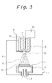
- An object for example, a tool to be treated or substrate is placed on a substrate holder 3 cooled by cooling water 2.
- a starting gas 8 is supplied between the anode and the cathode.
- a powder feed pipe 9 opens at the tip of the anode 6.
- a DC power source 10 is provided connecting the anode 6 and the cathode 7.
- At the bottom of the reaction chamber 4 is an exhaust outlet 11.
- a mixed gas of hydrogen (H 2 ) and a hydrocarbon, for example, methane (CH 4 ) is supplied from between the anode 6 and cathode 7 to the inside of the reaction chamber 4.
- the exhaust system is operated for exhaust from the exhaust outlet 11 and the inside of the reaction chamber 4 is held at a low vacuum, in which state an arc discharge 12 is caused between the anode 6 and cathode 7, the heat of which causes decomposition and plasmatization of the starting gas 8, whereupon the plasma jet 5 including carbon plasma strikes the metal plate 1 and a diamond film 13 composed of fine crystals is grown on the metal plate 1.
- a metal powder is supplied through the powder feed pipe 9 into the arc discharge 12, and to grow just a metal film, H 2 is used as the starting gas 8 and metal powder or inorganic material powder (e.g., silicon) is supplied through the powder feed pipe 9 into the arc discharge 12.
- metal powder or inorganic material powder e.g., silicon
- Figure 4 is a sectional view for explaining the present invention.
- the treated object 21 is a sintered body comprising WC or Mo 2 C, in which sintered body is dispersed a sintering reinforcement 23 such as cobalt (Co).
- the present invention has a first intermediate layer 24 composed of a mixture of the main component material (e.g., 99.9 - 90 wt%) of the treated object 1, i.e., WC or MoC, and the component elements of the diamond sintering reinforcement agent (e.g., 0.1 - 10 wt%), i.e., cobalt (Co), iron (Fe), nickel (Ni), and other transition metals.
- the second intermediate layer 25 is composed of a mixture of the component elements (e.g., 0.1 - 10 wt%) of the diamond sintering reinforcement agent, i.e., cobalt (Co), iron (Fe), nickel (Ni), and other transition metals and diamond (e.g., 99.9 - 90 wt%).
- the diamond film 22 is grown on the second intermediate layer 25.
- the three intermediate layers of (i) a first intermediate layer composed of (a) a component element (e.g., 99.9 - 90 wt%) of the object and (b) a component element (e.g., 0.1 - 10 wt%) of a sintering reinforcement agent for diamond, (ii) a second intermediate layer composed of a mixture of the materials of the first intermediate layer and (c) diamond (e.g., (b): 0.1 - 10 wt%, (a) + (c): 99.9 - 90 wt%, (a)/(c) 10/90 - 90/10), and (iii) a third intermediate layer composed of (b) a component element (e.g., 0.1 - 10 wt%) of the sintering reinforcement agent and (c) diamond (e.g., 99.9 - 90 wt%).
- a component element e.g., 99.9 - 90 wt%
- a component element e.g
- the present invention by providing at least two intermediate layers in this way, and gradually changing the composition of the treated object 21 and the diamond film 22, forms a diamond film 22 free from peeling even when formed to a thickness of about 100 ⁇ m.
- the preferable thickness of each intermediate layer is 2 to 10 ⁇ m, more preferably 4 to 8 ⁇ m and the preferable thickness of the diamond film is 10 to 100 ⁇ m, more preferably 20 to 40 ⁇ m.
- the size of the powder is preferably 0.1 to 8 ⁇ m, more preferably 0.4 to 1 ⁇ m.
- the surface, bottom, or entirety of a diamond film formed by the plasma jet chemical vapor deposition method is formed by a mixed phase comprised of component elements of metal bonding with said diamond film.
- the present invention uses the above-mentioned CVD apparatus to form a mixed phase of diamond and a bonding metal element on the surface, bottom, or entirety of the diamond film.
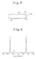
- Figure 5 is a sectional structural view of a diamond film in the case of use as a heat sink of a semiconductor device, wherein a mixed phase 29 of diamond and Cu is formed on the bottom surface 27 of the diamond film 26 which contacts a subcarrier 14 made of Cu and a top surface 28 contacting the semiconductor chip 16 in, for example, Fig. 2A.
- the diamond film formed by the CVD method is polycrystalline and therefore the shearing easily occurs at the crystalline interface and the crystal is relatively brittle, but since metal is interposed at the mixed phase, the mechanical strength is superior.
- the mixed phase may be just the bonded portion.
- the entire film may he formed by the mixed phase to eliminate the shearing.
- a flat or plain diamond film is formed on a substrate by the CVD method using a starting gas (e.g., H 2 , methane) for forming the diamond and a gas of an element for promoting formation of nuclei of the diamond such as reducing metals (e.g., Pt), carburizing metals (e.g., Ni, Co, Fe), or metals or semiconductors capable of easily forming carbides (e.g., W, Si, Mo, Ti).
- reducing metals e.g., Pt
- carburizing metals e.g., Ni, Co, Fe
- carbides e.g., W, Si, Mo, Ti
- a diamond coating is formed by simultaneously spraying or alternately spraying the above diamond forming a starting gas and diamond nucleus promoting element gas on the substrate by the CVD method or constantly spraying the starting gas and intermittently spraying the nucleus promoting element gas. That is, the method of the present invention, in the synthesis of diamond by the vapor phase synthesis method, sprays an element for promoting the formation of nuclei of diamond so as to generate large quantities of high density nuclei at the same time as the synthesis of the diamond film and thus suppresses the growth of specific crystal particles and gives a smooth or plain diamond film. Thus, the present invention tries to form a diamond coating using the above material gas by CVD.
- a diamond film having the desired high hardness can be formed on a substrate by exhausting a reaction chamber to vacuum by an exhaust system and while doing so supplying a mixed gas of a hydrocarbon gas and hydrogen gas between an anode and cathode provided in said reaction chamber, causing generation of a plasma jet of carbon by arc discharge, and forming a diamond film on the substrate, at which time adding a powder of an element of any one of tungsten (W), molybdenum (Mo), silicon (Si), or titanium (Ti), which can bond with the non-diamond carbon component in said plasma jet to form hard carbides.
- W tungsten
- Mo molybdenum
- Si silicon
- Ti titanium
- the present invention uses the plasma jet CVD apparatus shown in Fig. 3 to form a diamond film.
- powder of, for example, W, Mo, Si, Ti capable of forming hard carbides is added from a powder feed pipe and reacted with the amorphous carbon, graphite, and other nondiamond components to form hard carbides such as tungsten carbide (WC, hardness of 2200 kg/mm 2 ), molybdenum carbide (Mo 2 C, hardness of 1800 kg/mm 2 ), silicon carbide (SiC, hardness of 2300 kg/mm 2 ), titanium carbide (TiC, hardness of 3000 kg/mm 2 ), and the like.
- tungsten carbide WC, hardness of 2200 kg/mm 2
- Mo 2 C molybdenum carbide
- SiC silicon carbide
- TiC titanium carbide
- the carbon of, for example, the amorphous carbon, graphite is more active energywise compared with diamond, so selectively bonds with radicals of metal elements in the plasma state and form hard carbides.
- the present invention grows a diamond film by the plasma jet CVD method using a mixed gas of a hydrocarbon such as CH 4 and H 2 gas as a material gas and at that time changes the small amount of nondiamond components existing in the diamond polycrystalline layer due to the insufficient reduction and removal action of the H 2 gas to a hard carbide and thus improves the hardness.
- a mixed gas of a hydrocarbon such as CH 4 and H 2 gas
- a diamond film is formed on a substrate made of a carburizing material by forming a protective film on a substrate of a carburizing material by plasma injection using an element easily forming a carbide with a high melting point and then forming a diamond film over the protective film by plasma CVD.
- the present invention enables, in the synthesis of diamond by the vapor phase synthesis method, the coating of a diamond film on a carburizing base material by providing a coating film facilitating the synthesis of diamond on the surface of the base material.
- Examples of the carburizing material usable in the present invention are Fe, Ni, Co, and other metals. Further, as the element easily forming a carbide with a high melting point, use is preferably made of WC, Si, Mo, W, or other elements. It is possible to use these materials and to work the method of the present invention using the same apparatus, as clear from the later mentioned examples.
- a diamond film is uniformly and firmly deposited on an object or substrate even on the side surfaces thereof as shown in Figs. 10 to 12.
- the object 1 is rotated and is inclined from the flow direction line of the plasma jet 5 by 30 to 60 degree (see ⁇ in Fig. 10), whereby the intermediate layers and the diamond film are uniformly and firmly deposited on the side faces 30 of the object 1.
- the intermediate layer 39 and the diamond film 40 are deposited on the side surfaces 30 of the object 1, the side surfaces 30 are not well covered by the intermediate layers 39, because the plasma jet 5 does not arrive at the side surfaces 30. Accordingly, the diamond film 40 is sometimes directly deposited on the side surfaces 39 as shown in Fig. 11. Thus, the diamond film 40 on the side surfaces 30 tends to be easily peeled off or cracks sometimes occur between the intermediate layer 30 and the diamond film 40 especially at the end portions of the object 1.
- a first intermediate layer 41 having a thickness of, for example, 2 - 5 ⁇ m is formed by introducing a powder of, for example, WC (the same material as the object), from a pipe 9 to a plasma jet 5 formed from hydrogen gas or an inert gas
- a second intermediate layer 42 having a thickness of, for example, 10 - 20 ⁇ m is formed by introducing a powder of WC and a powder of, for example, Fe, Co, Ni, Nb and/or Ta, from a pipe 9 to the plasma jet 5 generated from hydrogen gas and a carbon source
- a third intermediate layer 43 having a thickness of, for example, 20 - 30 ⁇ m is formed by introducing a powder of, for example, Fe, Co, Ni, Nb and/or Ta (the same metal used in the formation of the second intermediate layer 42) from a pipe to a plasma jet 5, generated from hydrogen gas and a carbon source (e.g., hydrocarbon gas such as methane).
- the inclination and rotation of the object (or substrate) 1 can be effected in any conventional manner.
- the supporting means 31 of the object (or substrate) 1 is composed of a cooled support 32 for the object 1, a motor 34 provided with a rotating shaft 33 for rotating the support 32, a movable base 35 for carrying the motor 34, and an arc-shaped guide member 36 for moving the movable base 35 so that the surface, to be coated, of the object 1 is inclined at an angle of ⁇ .
- the object 1 is moved so that it is inclined from the plasma jet flow direction, the plasma torch can also be moved in the similar manner.
- a sintered body using Co as a sintering reinforcement and having a composition of WC-10% Co was used.
- As the conditions for growth of the second intermediate layer and diamond film the CVD apparatus shown in Fig. 3 was used and H 2 gas of 10 to 50 liter/min and CH 4 gas of 0.05 to 1 liter/min were supplied. Further, an arc current of 10 to 70 A and an arc voltage changed in a range of 50 to 150 V were used. The vacuum of the reaction chamber was held in the range of 1 to 10 kPa.
- H 2 gas was supplied as the starting gas and a plasma jet generated, in which state WC and Co of a particle size of 1 to 5 ⁇ m were supplied from the powder feed pipe 9 at a rate of 0.01 to 0.1 cc/h and plasmatized to grow a mixture at a thickness of 20 ⁇ m.
- the material gas was changed to a mixed gas of H 2 and CH 4 and Co powder of a particle size of 1 to 5 ⁇ m was supplied from the powder feed pipe 9 to create a plasma jet and form a second intermediate layer comprised of a mixture of diamond and Co at a thickness of 30 ⁇ m.
- Figure 6 is an X-ray diffraction pattern of the second intermediate layer, where the diffraction lines of diamond (abbreviated as D) and Co appear well, so it is understood that a mixed layer is grown. Then, a plasma jet is created using a mixed gas of H 2 and CH 4 as a material gas and a diamond film of a thickness of about 100 ⁇ m is formed on the top. The adhesiveness with the treated object of the diamond film formed in this way is strong. A tensile test gave a value of more than 600 kg/mm 2 .
- the CVD apparatus shown in Fig. 3 was used and a starting gas 8 composed of hydrogen (H 2 ) gas changed in flow from 10 to 50 liter/min and methane gas (CH 4 ) changed in flow from 0.05 to 1 liter/min was supplied. Further, metallic powder comprised of Cu powder with a particle size of 1 to 5 ⁇ m was supplied using a powder feed pipe 9 at a rate of 0.01 to 0.1 cc/h.
- H 2 hydrogen
- CH 4 methane gas
- a diamond film 13 is formed and when metal particulates are mixed in, a mixed phase of diamond and metal is formed. Further, when H 2 gas and a metal powder were used, a metal film is formed. Then, the conditions for causing CVD growth are a vacuum of the reaction chamber 4 of 1 kPa to 10 kPa, an arc current of 10 to 70 A, and an arc voltage of 50 to 150 V. Thus, there was formed a diamond film of a thickness of 50 ⁇ m having a mixed phase of Cu of a thickness of 1 ⁇ m with a ratio of composition of the top surface and bottom surface of about 5:1. Then, using this diamond film as a heat sink and using solder with a melting point of 250°C to bond this with the subcarrier or bond a laser diode on top of it, it was possible to solder with a sufficient bonding strength.
- hydrogen gas, methane gas, or other starting gas 8 is introduced from the top of the plasma torch in the reaction chamber and made into plasma by DC arc discharge. That plasma 5 reacts on the substrate 1 to form a diamond film 13.
- metal particulates may be introduced along with the material gas and metal vapor sprayed on the diamond surface.
- 10 to 50 liter/min of hydrogen gas, 0.05 to 1 liter/min of methane gas, and a substrate of WC of a thickness of 0.5 mm and a surface area of 10 x 10 mm 2 were used.
- the spraying powder material 0.001 to 0.0001 cc of 1 to 5 ⁇ m particulates of W is supplied each time the thickness of the diamond film increases 0.1 mm.
- the arc current is 10 to 70 A and the arc discharge is 50 to 150 V.
- the degree of vacuum of the reaction chamber is 1 k to 10 kPa. As a result, even with a diamond film of a thickness of 2 mm, the surface roughness is less than 0.05 mm.
- Diamond films were synthesized under the same synthesis conditions but with different types of metal particulates and the surface roughness was measured. The results are shown in Table 1.
- the CVD apparatus shown in Fig. 3 was used and a superhard alloy of W including 8% Co as the metal plate 1.
- the flow of hydrogen (H 2 ) gas was changed between a range of 10 to 50 liter/min and the flow of methane (CH 4 ) gas a range of 0.05 to 1 liter/min and, as a metal powder, a powder of W of 1 to 5 ⁇ m particle size was supplied at a rate of 0.01 to 0.1 cc/h.
- the conditions where CVD were possible were a vacuum of the reaction chamber 4 of 1 kPa to 10 kPa, an arc current of 10 to 70 A, and an arc voltage of 50 to 150 V.
- Figure 7 shows the Raman spectrum 30 of the film obtained by supplying W as the additive and the Raman spectrum 31 of the film with no additive. As will be understood from Fig. 7, a broad peak of amorphous carbon was observed near 1500 cm -1 in the spectrum of the film with no additive.
- the hardness of the diamond film formed in this way is about 10,000 kg/mm 2 , close to that of natural diamond.
- a substrate 1 of Ni of a thickness of 0.5 mm use was made of a substrate 1 of Ni of a thickness of 0.5 mm and an inert gas (or hydrogen) was introduced into the plasma torch in the reaction chamber 4 at a flow rate of 10 to 50 liter/min. Then, using an arc current of 10 to 70 A and an arc voltage of 50 to 150 V, the inert gas was subjected to arc discharge and converted to plasma. Note that the vacuum in the reaction chamber was 1 k to 10 kPa.
- WC particulates of 1 to 5 ⁇ m were supplied from a powder feed apparatus at a rate of 0.01 to 0.1 cc/h.
- the WC particulates were melted by the high temperature plasma and together with the plasma jet 5 deposited on the substrate 1 to form the protective film.
- the flow rates of feed of the methane gas and hydrogen gas were respectively 0.05 to 1 liter/min and 10 liter/min to 100 liter/min.
- the starting gas was converted to plasma by the DC arc discharge 12 at the same time and the plasma jet 5 deposited on the protective film to form the diamond film 13.
- the diamond film obtained by the method of the present invention was subjected to X-ray analysis and the pattern found. The pattern was shown in Fig. 8. As clear from the pattern, there were simultaneously a pattern of a protective film and a pattern of diamond and it was observed a diamond film was definitely synthesized.
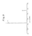
- X ray analysis was performed on a substrate without a protective film. Its pattern is shown in Fig. 9. As clear from this Fig. 9, only the pattern of the substrate (Ni) was observed and no pattern of diamond was observed, so it was confirmed that no diamond film was synthesized.
- a diamond film having superior adhesiveness can be coated on a treated object, so it is possible to provide a diamond tool with a high reliability.
- the present invention by using a CVD apparatus which can form a mixed phase of a diamond film and metal by CVD growth changing the combination of the type of starting gas and metal powder and working the present invention wherein the surface, bottom, or entirety of the diamond film is made by the mixed phase, it is possible to obtain a diamond film superior adhesiveness at a low cost.
- the method of the present invention uses a gas of a predetermined material to form a diamond film by the CVD method, so there is the effect that it is possible to considerably improve the smoothness of the surface of thick diamond film, reduce working costs, and raise work efficiency.
- the present invention it is easy to synthesize a diamond film with little amorphous carbon, graphite, or other nondiamond components and, by working the invention, to provide diamond tools at low cost.
- the present invention is further constituted so as to form a protective film of a predetermined material on a substrate and then synthesize a diamond film, so exhibits the effect of enabling coating of a diamond film on a carburizing base material, which was previously impossible.
Landscapes
- Chemical & Material Sciences (AREA)
- Engineering & Computer Science (AREA)
- Metallurgy (AREA)
- Chemical Kinetics & Catalysis (AREA)
- Materials Engineering (AREA)
- Mechanical Engineering (AREA)
- Organic Chemistry (AREA)
- General Chemical & Material Sciences (AREA)
- Inorganic Chemistry (AREA)
- Physics & Mathematics (AREA)
- Plasma & Fusion (AREA)
- Combustion & Propulsion (AREA)
- Crystals, And After-Treatments Of Crystals (AREA)
- Chemical Vapour Deposition (AREA)
Claims (8)
- Verfahren zur Bildung einer Diamantbeschichtung auf einem Substrat, welches das Synthetisieren eines Diamantfilms auf dem Substrat durch das CVD-Verfahren unter Verwendung von einem Gas eines Materials zur Bildung von Diamant und Pulvern eines Elements zur Förderung der Bildung von Diamantnuklei umfaßt, wobei der Diamantfilm durch ein Verfahren gebildet wird, das die Schritte umfaßt:Bewirken einer Bogenentladung, während ein Wasserstoff und eine Kohlenstoffquelle enthaltendes Entladungsgas zwischen einer Anode und einer Kathode einer thermischen Plasma/chemischen Dampfabscheidungsvorrichtung zugeführt wird;Radikalisieren einer gasförmigen Kohlenstoffverbindung, indem die gasförmige Verbindung einem erzeugten Plasmastrahl zugeführt wird, worin die Wasserstoffmoleküle im wesentlichen in Wasserstoffatome dissoziiert werden, während ein Pulver eines Elements zur Förderung der Bildung von Diamantnuklei zugeführt wird; undAuftreffenlassen des radikalisierten Plasmastrahls auf dem zu behandelnden Objekt, um dadurch einen Diamantfilm auf dem Objekt zu bilden.
- Verfahren nach Anspruch 1, bei welchem das Element zur Förderung der Bildung von Diamantnuklei zumindest ein Element ist, das aus der Gruppe bestehend aus Reduktionsmetallen, Carburierungsmetallen und Metallen, die leicht Carbide bilden können, sowie Halbleitern, die leicht Carbide bilden können, ausgewählt wird.
- Verfahren nach Anspruch 2, bei welchem das Reduktionsmetall Platin ist.
- Verfahren nach Anspruch 2 oder 3, bei welchem die Carburierungsmetalle Nickel, Cobalt und Eisen sind.
- Verfahren nach Anspruch 2, 3 oder 4, bei welchem die Metalle und Halbleiter, die leicht Carbide bilden können, Wolfram, Silicium, Titan und Molybdän sind.
- Verfahren zur Synthese eines Diamantfilms, welches die Schritte umfaßt:wobei der Schutzfilm durch ein Verfahren gebildet wird, das, während ein Plasmastrahl aus einem Inertgas oder Wasserstoff erzeugt wird, das Zuführen eines Pulvers des Elements in den Plasmastrahl umfaßt;(i) Bilden eines Schutzfilms auf einem Substrat eines Carburierungsmaterials durch Plasmainjektion unter Verwendung eines Elements, das leicht ein Carbid mit einem hohen Schmelzpunkt bilden kann; und dann(ii) Bilden eines Diamantfilms über dem Schutzfilm durch ein Plasma-CVD-Verfahren:
und wobei der Diamantfilm durch ein Verfahren gebildet wird, das die Schritte umfaßt:
Bewirken einer Bogenentladung, während ein Wasserstoff und eine Kohlenstoffquelle enthaltendes Entladungsgas zwischen einer Anode und einer Kathode einer thermischen Plasma/chemischen Dampfabscheidungsvorrichtung zugeführt wird;
Radikalisieren einer gasförmigen Kohlenstoffverbindung, indem die gasförmige Verbindung einem erzeugten Plasmastrahl zugeführt wird, worin die Wasserstoffmoleküle im wesentlichen in Wasserstoffatome dissoziiert werden; und
Auftreffenlassen des radikalisierten Plasmastrahls auf dem zu behandelnden Objekt, um dadurch einen Diamantfilm auf dem Objekt zu bilden. - Verfahren nach Anspruch 6, bei welchem das Element, das leicht ein Carbid bilden kann, zumindest ein Element ist, das aus der Gruppe bestehend aus Silicium, Molybdän, Titan und Wolfram ausgewählt wird.
- Diamantfilm auf einem Substrat, welcher durch das Verfahren nach einem der Ansprüche 1 bis 7 erhalten wird.
Priority Applications (1)
| Application Number | Priority Date | Filing Date | Title |
|---|---|---|---|
| DE1990632901 DE69032901T2 (de) | 1990-08-03 | 1990-08-03 | Verfahren zur Diamantabscheidung mittels CVD |
Applications Claiming Priority (1)
| Application Number | Priority Date | Filing Date | Title |
|---|---|---|---|
| EP19900308570 EP0469204B1 (de) | 1990-08-03 | 1990-08-03 | Verfahren zur Abscheidung aus der Gasphase eines Diamantfilmes |
Related Parent Applications (2)
| Application Number | Title | Priority Date | Filing Date |
|---|---|---|---|
| EP90308570.2 Division | 1990-08-03 | ||
| EP19900308570 Division EP0469204B1 (de) | 1990-08-03 | 1990-08-03 | Verfahren zur Abscheidung aus der Gasphase eines Diamantfilmes |
Publications (2)
| Publication Number | Publication Date |
|---|---|
| EP0721998A1 EP0721998A1 (de) | 1996-07-17 |
| EP0721998B1 true EP0721998B1 (de) | 1999-01-13 |
Family
ID=8205509
Family Applications (2)
| Application Number | Title | Priority Date | Filing Date |
|---|---|---|---|
| EP96100465A Expired - Lifetime EP0721998B1 (de) | 1990-08-03 | 1990-08-03 | Verfahren zur Diamantabscheidung mittels CVD |
| EP19900308570 Expired - Lifetime EP0469204B1 (de) | 1990-08-03 | 1990-08-03 | Verfahren zur Abscheidung aus der Gasphase eines Diamantfilmes |
Family Applications After (1)
| Application Number | Title | Priority Date | Filing Date |
|---|---|---|---|
| EP19900308570 Expired - Lifetime EP0469204B1 (de) | 1990-08-03 | 1990-08-03 | Verfahren zur Abscheidung aus der Gasphase eines Diamantfilmes |
Country Status (2)
| Country | Link |
|---|---|
| EP (2) | EP0721998B1 (de) |
| DE (1) | DE69029729T2 (de) |
Families Citing this family (9)
| Publication number | Priority date | Publication date | Assignee | Title |
|---|---|---|---|---|
| DE4112156A1 (de) * | 1991-04-13 | 1992-10-15 | Lugscheider Erich | Mit hilfe eines plasmabrenners aufgebrachte beschichtung sowie plasmabrenner |
| US5260141A (en) * | 1991-11-29 | 1993-11-09 | Regents Of The University Of Minnesota | Diamond coated products |
| DE69332263T2 (de) * | 1992-06-30 | 2003-08-07 | Sumitomo Electric Industries, Ltd. | Schneidwerkzeug unter Anwendung von aus der Dampfphase abgeschiedenem polykristallinem Diamant für die Schneidkante und Verfahren zu dessen Herstellung |
| US5909879A (en) * | 1993-03-09 | 1999-06-08 | Norton Company | Diamond film coating for mating parts |
| PL314108A1 (en) * | 1993-10-29 | 1996-08-19 | Balzers Hochvakuum | Coated formpiece, method of making same and application thereof |
| GB9405029D0 (en) * | 1994-03-15 | 1994-04-27 | Franks Joseph Dr | Improved catheters and other tubular inserts |
| JP4560964B2 (ja) * | 2000-02-25 | 2010-10-13 | 住友電気工業株式会社 | 非晶質炭素被覆部材 |
| DE10018143C5 (de) * | 2000-04-12 | 2012-09-06 | Oerlikon Trading Ag, Trübbach | DLC-Schichtsystem sowie Verfahren und Vorrichtung zur Herstellung eines derartigen Schichtsystems |
| CN112779599B (zh) * | 2020-12-23 | 2022-11-18 | 济南金刚石科技有限公司 | 亚微米级金刚石薄膜的化学气相沉积方法及装置 |
Family Cites Families (6)
| Publication number | Priority date | Publication date | Assignee | Title |
|---|---|---|---|---|
| DE3706340A1 (de) * | 1987-02-27 | 1988-09-08 | Winter & Sohn Ernst | Verfahren zum auftragen einer verschleissschutzschicht und danach hergestelltes erzeugnis |
| EP0286306B1 (de) * | 1987-04-03 | 1993-10-06 | Fujitsu Limited | Verfahren und Vorrichtung zur Gasphasenabscheidung von Diamant |
| JPH085747B2 (ja) * | 1987-08-26 | 1996-01-24 | 住友電気工業株式会社 | 超硬質多結晶体の製造法 |
| KR920000801B1 (ko) * | 1988-02-04 | 1992-01-23 | 이데미쯔세끼유가가꾸 가부시기가이샤 | 다이아몬드박막부착 초경합금의 제조방법 |
| JPH0794360B2 (ja) * | 1989-01-24 | 1995-10-11 | 住友電気工業株式会社 | ダイヤモンドの気相合成法 |
| JP2620976B2 (ja) * | 1989-07-07 | 1997-06-18 | 株式会社豊田中央研究所 | 摺動部材 |
-
1990
- 1990-08-03 EP EP96100465A patent/EP0721998B1/de not_active Expired - Lifetime
- 1990-08-03 EP EP19900308570 patent/EP0469204B1/de not_active Expired - Lifetime
- 1990-08-03 DE DE1990629729 patent/DE69029729T2/de not_active Expired - Fee Related
Also Published As
| Publication number | Publication date |
|---|---|
| EP0721998A1 (de) | 1996-07-17 |
| EP0469204A1 (de) | 1992-02-05 |
| DE69029729T2 (de) | 1997-05-07 |
| DE69029729D1 (de) | 1997-02-27 |
| EP0469204B1 (de) | 1997-01-15 |
Similar Documents
| Publication | Publication Date | Title |
|---|---|---|
| US5382293A (en) | Plasma jet CVD apparatus for forming diamond films | |
| EP0378378B1 (de) | Herstellung von diamantverbundbeschichteten Schneidwerkzeugen | |
| US5435815A (en) | Cutting tool employing vapor-deposited polycrystalline diamond for cutting edge and method of manufacturing the same | |
| CA1336704C (en) | Method of producing sintered hard metal with diamond film | |
| JPH0418975B2 (de) | ||
| WO1995027806A1 (en) | Process to produce diamond films | |
| EP0413834A1 (de) | Mit diamanten bedecktes glied und verfahren zur herstellung | |
| EP0721998B1 (de) | Verfahren zur Diamantabscheidung mittels CVD | |
| US7645513B2 (en) | Cubic boron nitride/diamond composite layers | |
| US5492770A (en) | Method and apparatus for vapor deposition of diamond film | |
| US20050016444A1 (en) | Method for diamond coating substrates | |
| Kikuchi et al. | Characteristics of thin film growth in the synthesis of diamond by chemical vapour deposition and application of the thin film synthesis technology for tools | |
| KR930011165B1 (ko) | 다이아몬드막의 기상증착법 및 그 장치 | |
| US5567522A (en) | Diamond cutting tool and method of manufacturing the same | |
| JPH05263251A (ja) | 被覆焼結体 | |
| JP3235206B2 (ja) | ダイヤモンド切削工具およびその製造方法 | |
| JPH0671503A (ja) | ダイヤモンド切削工具およびその製造方法 | |
| JP3134378B2 (ja) | ダイヤモンド被覆硬質材料 | |
| JPH08151297A (ja) | ダイヤモンドの製造方法 | |
| JP2686970B2 (ja) | 膜状ダイヤモンドの製造方法 | |
| JPH0623431B2 (ja) | 硬質被膜被覆切削工具部材 | |
| JP2629939B2 (ja) | ダイヤモンド膜の製造方法 | |
| JPH0582474B2 (de) | ||
| JP2762561B2 (ja) | ダイヤモンド膜の合成方法 | |
| JP3346654B2 (ja) | ダイヤモンド−タングステン複合膜付部材 |
Legal Events
| Date | Code | Title | Description |
|---|---|---|---|
| PUAI | Public reference made under article 153(3) epc to a published international application that has entered the european phase |
Free format text: ORIGINAL CODE: 0009012 |
|
| 17P | Request for examination filed |
Effective date: 19960116 |
|
| AC | Divisional application: reference to earlier application |
Ref document number: 469204 Country of ref document: EP |
|
| AK | Designated contracting states |
Kind code of ref document: A1 Designated state(s): DE GB |
|
| 17Q | First examination report despatched |
Effective date: 19970521 |
|
| GRAG | Despatch of communication of intention to grant |
Free format text: ORIGINAL CODE: EPIDOS AGRA |
|
| GRAG | Despatch of communication of intention to grant |
Free format text: ORIGINAL CODE: EPIDOS AGRA |
|
| GRAH | Despatch of communication of intention to grant a patent |
Free format text: ORIGINAL CODE: EPIDOS IGRA |
|
| RBV | Designated contracting states (corrected) |
Designated state(s): DE GB |
|
| GRAH | Despatch of communication of intention to grant a patent |
Free format text: ORIGINAL CODE: EPIDOS IGRA |
|
| GRAA | (expected) grant |
Free format text: ORIGINAL CODE: 0009210 |
|
| AC | Divisional application: reference to earlier application |
Ref document number: 469204 Country of ref document: EP |
|
| AK | Designated contracting states |
Kind code of ref document: B1 Designated state(s): DE GB |
|
| REF | Corresponds to: |
Ref document number: 69032901 Country of ref document: DE Date of ref document: 19990225 |
|
| RIN2 | Information on inventor provided after grant (corrected) |
Free format text: KAWARADA, MOTONOBU * KURIHARA, KAZUAKI * SASAKI, KEN-ICHI * TESHIMA, AKITOMO * KOSHINO, NAGAAKI |
|
| PLBE | No opposition filed within time limit |
Free format text: ORIGINAL CODE: 0009261 |
|
| STAA | Information on the status of an ep patent application or granted ep patent |
Free format text: STATUS: NO OPPOSITION FILED WITHIN TIME LIMIT |
|
| 26N | No opposition filed | ||
| REG | Reference to a national code |
Ref country code: GB Ref legal event code: IF02 |
|
| PGFP | Annual fee paid to national office [announced via postgrant information from national office to epo] |
Ref country code: DE Payment date: 20050728 Year of fee payment: 16 |
|
| PGFP | Annual fee paid to national office [announced via postgrant information from national office to epo] |
Ref country code: GB Payment date: 20050803 Year of fee payment: 16 |
|
| PG25 | Lapsed in a contracting state [announced via postgrant information from national office to epo] |
Ref country code: DE Free format text: LAPSE BECAUSE OF NON-PAYMENT OF DUE FEES Effective date: 20070301 |
|
| GBPC | Gb: european patent ceased through non-payment of renewal fee |
Effective date: 20060803 |
|
| PG25 | Lapsed in a contracting state [announced via postgrant information from national office to epo] |
Ref country code: GB Free format text: LAPSE BECAUSE OF NON-PAYMENT OF DUE FEES Effective date: 20060803 |