EP0722077A2 - Appareil de traitement d'informations avec contrÔle de la position par forces électrostatiques - Google Patents
Appareil de traitement d'informations avec contrÔle de la position par forces électrostatiques Download PDFInfo
- Publication number
- EP0722077A2 EP0722077A2 EP96100370A EP96100370A EP0722077A2 EP 0722077 A2 EP0722077 A2 EP 0722077A2 EP 96100370 A EP96100370 A EP 96100370A EP 96100370 A EP96100370 A EP 96100370A EP 0722077 A2 EP0722077 A2 EP 0722077A2
- Authority
- EP
- European Patent Office
- Prior art keywords
- probe
- information processing
- processing apparatus
- electrodes
- distance
- Prior art date
- Legal status (The legal status is an assumption and is not a legal conclusion. Google has not performed a legal analysis and makes no representation as to the accuracy of the status listed.)
- Granted
Links
- 239000000523 sample Substances 0.000 title claims abstract description 120
- 230000010365 information processing Effects 0.000 title claims abstract description 15
- 230000010399 physical interaction Effects 0.000 claims abstract description 9
- 238000001514 detection method Methods 0.000 claims abstract description 5
- 230000000694 effects Effects 0.000 claims description 9
- 230000001276 controlling effect Effects 0.000 claims 1
- 230000001105 regulatory effect Effects 0.000 claims 1
- 239000003990 capacitor Substances 0.000 description 20
- 238000006243 chemical reaction Methods 0.000 description 20
- 239000000758 substrate Substances 0.000 description 18
- 238000000034 method Methods 0.000 description 13
- 229920002120 photoresistant polymer Polymers 0.000 description 8
- 239000010410 layer Substances 0.000 description 7
- 230000033001 locomotion Effects 0.000 description 7
- XLOMVQKBTHCTTD-UHFFFAOYSA-N Zinc monoxide Chemical compound [Zn]=O XLOMVQKBTHCTTD-UHFFFAOYSA-N 0.000 description 6
- 238000006073 displacement reaction Methods 0.000 description 6
- 238000005530 etching Methods 0.000 description 6
- 238000010586 diagram Methods 0.000 description 5
- 230000007246 mechanism Effects 0.000 description 5
- 238000002360 preparation method Methods 0.000 description 5
- 229910052581 Si3N4 Inorganic materials 0.000 description 4
- 239000010408 film Substances 0.000 description 4
- 238000004518 low pressure chemical vapour deposition Methods 0.000 description 4
- 239000000463 material Substances 0.000 description 4
- HQVNEWCFYHHQES-UHFFFAOYSA-N silicon nitride Chemical compound N12[Si]34N5[Si]62N3[Si]51N64 HQVNEWCFYHHQES-UHFFFAOYSA-N 0.000 description 4
- 238000004544 sputter deposition Methods 0.000 description 4
- QTBSBXVTEAMEQO-UHFFFAOYSA-N Acetic acid Chemical compound CC(O)=O QTBSBXVTEAMEQO-UHFFFAOYSA-N 0.000 description 3
- KWYUFKZDYYNOTN-UHFFFAOYSA-M Potassium hydroxide Chemical compound [OH-].[K+] KWYUFKZDYYNOTN-UHFFFAOYSA-M 0.000 description 3
- 230000008859 change Effects 0.000 description 3
- 230000010354 integration Effects 0.000 description 3
- 239000011159 matrix material Substances 0.000 description 3
- 230000015654 memory Effects 0.000 description 3
- 230000003446 memory effect Effects 0.000 description 3
- 238000005070 sampling Methods 0.000 description 3
- 239000004065 semiconductor Substances 0.000 description 3
- 239000000126 substance Substances 0.000 description 3
- 239000011787 zinc oxide Substances 0.000 description 3
- CSCPPACGZOOCGX-UHFFFAOYSA-N Acetone Chemical compound CC(C)=O CSCPPACGZOOCGX-UHFFFAOYSA-N 0.000 description 2
- QGZKDVFQNNGYKY-UHFFFAOYSA-N Ammonia Chemical compound N QGZKDVFQNNGYKY-UHFFFAOYSA-N 0.000 description 2
- MHAJPDPJQMAIIY-UHFFFAOYSA-N Hydrogen peroxide Chemical compound OO MHAJPDPJQMAIIY-UHFFFAOYSA-N 0.000 description 2
- VYPSYNLAJGMNEJ-UHFFFAOYSA-N Silicium dioxide Chemical compound O=[Si]=O VYPSYNLAJGMNEJ-UHFFFAOYSA-N 0.000 description 2
- XUIMIQQOPSSXEZ-UHFFFAOYSA-N Silicon Chemical compound [Si] XUIMIQQOPSSXEZ-UHFFFAOYSA-N 0.000 description 2
- 239000007864 aqueous solution Substances 0.000 description 2
- 239000004020 conductor Substances 0.000 description 2
- 238000012937 correction Methods 0.000 description 2
- 239000013078 crystal Substances 0.000 description 2
- 229910052751 metal Inorganic materials 0.000 description 2
- 239000002184 metal Substances 0.000 description 2
- 238000001020 plasma etching Methods 0.000 description 2
- 230000008569 process Effects 0.000 description 2
- 230000004044 response Effects 0.000 description 2
- 229910052710 silicon Inorganic materials 0.000 description 2
- 239000010703 silicon Substances 0.000 description 2
- 229910052814 silicon oxide Inorganic materials 0.000 description 2
- 230000004304 visual acuity Effects 0.000 description 2
- 229910001218 Gallium arsenide Inorganic materials 0.000 description 1
- 230000004075 alteration Effects 0.000 description 1
- 229910021529 ammonia Inorganic materials 0.000 description 1
- 238000005452 bending Methods 0.000 description 1
- -1 chalcogenide compounds Chemical class 0.000 description 1
- 238000011161 development Methods 0.000 description 1
- 238000010894 electron beam technology Methods 0.000 description 1
- 230000006870 function Effects 0.000 description 1
- 239000007789 gas Substances 0.000 description 1
- 239000011521 glass Substances 0.000 description 1
- 229910052737 gold Inorganic materials 0.000 description 1
- 238000005259 measurement Methods 0.000 description 1
- 239000010445 mica Substances 0.000 description 1
- 229910052618 mica group Inorganic materials 0.000 description 1
- 239000011259 mixed solution Substances 0.000 description 1
- 229910021421 monocrystalline silicon Inorganic materials 0.000 description 1
- 150000002894 organic compounds Chemical class 0.000 description 1
- 229910052697 platinum Inorganic materials 0.000 description 1
- 238000012545 processing Methods 0.000 description 1
- 239000011241 protective layer Substances 0.000 description 1
- 230000000717 retained effect Effects 0.000 description 1
- 239000000243 solution Substances 0.000 description 1
- 239000010409 thin film Substances 0.000 description 1
- 238000007738 vacuum evaporation Methods 0.000 description 1
Images


Classifications
-
- G—PHYSICS
- G01—MEASURING; TESTING
- G01Q—SCANNING-PROBE TECHNIQUES OR APPARATUS; APPLICATIONS OF SCANNING-PROBE TECHNIQUES, e.g. SCANNING PROBE MICROSCOPY [SPM]
- G01Q10/00—Scanning or positioning arrangements, i.e. arrangements for actively controlling the movement or position of the probe
- G01Q10/04—Fine scanning or positioning
- G01Q10/06—Circuits or algorithms therefor
- G01Q10/065—Feedback mechanisms, i.e. wherein the signal for driving the probe is modified by a signal coming from the probe itself
-
- B—PERFORMING OPERATIONS; TRANSPORTING
- B82—NANOTECHNOLOGY
- B82Y—SPECIFIC USES OR APPLICATIONS OF NANOSTRUCTURES; MEASUREMENT OR ANALYSIS OF NANOSTRUCTURES; MANUFACTURE OR TREATMENT OF NANOSTRUCTURES
- B82Y35/00—Methods or apparatus for measurement or analysis of nanostructures
-
- G—PHYSICS
- G11—INFORMATION STORAGE
- G11B—INFORMATION STORAGE BASED ON RELATIVE MOVEMENT BETWEEN RECORD CARRIER AND TRANSDUCER
- G11B9/00—Recording or reproducing using a method not covered by one of the main groups G11B3/00 - G11B7/00; Record carriers therefor
- G11B9/12—Recording or reproducing using a method not covered by one of the main groups G11B3/00 - G11B7/00; Record carriers therefor using near-field interactions; Record carriers therefor
- G11B9/14—Recording or reproducing using a method not covered by one of the main groups G11B3/00 - G11B7/00; Record carriers therefor using near-field interactions; Record carriers therefor using microscopic probe means, i.e. recording or reproducing by means directly associated with the tip of a microscopic electrical probe as used in Scanning Tunneling Microscopy [STM] or Atomic Force Microscopy [AFM] for inducing physical or electrical perturbations in a recording medium; Record carriers or media specially adapted for such transducing of information
- G11B9/1418—Disposition or mounting of heads or record carriers
- G11B9/1427—Disposition or mounting of heads or record carriers with provision for moving the heads or record carriers relatively to each other or for access to indexed parts without effectively imparting a relative movement
- G11B9/1436—Disposition or mounting of heads or record carriers with provision for moving the heads or record carriers relatively to each other or for access to indexed parts without effectively imparting a relative movement with provision for moving the heads or record carriers relatively to each other
- G11B9/1445—Disposition or mounting of heads or record carriers with provision for moving the heads or record carriers relatively to each other or for access to indexed parts without effectively imparting a relative movement with provision for moving the heads or record carriers relatively to each other switching at least one head in operating function; Controlling the relative spacing to keep the head operative, e.g. for allowing a tunnel current flow
-
- G—PHYSICS
- G01—MEASURING; TESTING
- G01Q—SCANNING-PROBE TECHNIQUES OR APPARATUS; APPLICATIONS OF SCANNING-PROBE TECHNIQUES, e.g. SCANNING PROBE MICROSCOPY [SPM]
- G01Q80/00—Applications, other than SPM, of scanning-probe techniques
-
- Y—GENERAL TAGGING OF NEW TECHNOLOGICAL DEVELOPMENTS; GENERAL TAGGING OF CROSS-SECTIONAL TECHNOLOGIES SPANNING OVER SEVERAL SECTIONS OF THE IPC; TECHNICAL SUBJECTS COVERED BY FORMER USPC CROSS-REFERENCE ART COLLECTIONS [XRACs] AND DIGESTS
- Y10—TECHNICAL SUBJECTS COVERED BY FORMER USPC
- Y10S—TECHNICAL SUBJECTS COVERED BY FORMER USPC CROSS-REFERENCE ART COLLECTIONS [XRACs] AND DIGESTS
- Y10S977/00—Nanotechnology
- Y10S977/84—Manufacture, treatment, or detection of nanostructure
- Y10S977/849—Manufacture, treatment, or detection of nanostructure with scanning probe
- Y10S977/85—Scanning probe control process
- Y10S977/851—Particular movement or positioning of scanning tip
-
- Y—GENERAL TAGGING OF NEW TECHNOLOGICAL DEVELOPMENTS; GENERAL TAGGING OF CROSS-SECTIONAL TECHNOLOGIES SPANNING OVER SEVERAL SECTIONS OF THE IPC; TECHNICAL SUBJECTS COVERED BY FORMER USPC CROSS-REFERENCE ART COLLECTIONS [XRACs] AND DIGESTS
- Y10—TECHNICAL SUBJECTS COVERED BY FORMER USPC
- Y10S—TECHNICAL SUBJECTS COVERED BY FORMER USPC CROSS-REFERENCE ART COLLECTIONS [XRACs] AND DIGESTS
- Y10S977/00—Nanotechnology
- Y10S977/84—Manufacture, treatment, or detection of nanostructure
- Y10S977/849—Manufacture, treatment, or detection of nanostructure with scanning probe
- Y10S977/86—Scanning probe structure
- Y10S977/872—Positioner
Definitions
- the present invention relates to an information processing apparatus effecting information processing by physical interaction between a probe and a recording medium, such as a recording/reproducing apparatus or a scanning tunnel microscope (STM).
- a recording/reproducing apparatus such as a recording/reproducing apparatus or a scanning tunnel microscope (STM).
- STM scanning tunnel microscope
- the STM utilizes the tunnelling current, generated when a probe having a metal tip and a conductive substance are brought to a small distance of about 1 nm, with a voltage applied therebetween.
- This current is extremely sensitive to the distance between the both, and various information on the entire electron cloud in the real space can be read by moving the tip in a scanning motion so as to maintain the tunnelling current constant. In such operation, there can be obtained a resolving power of about 0.1 nm, in the longitudinal direction along the surface of the conductive substance.
- an information recording/reproducing apparatus disclosed in the Japanese Patent Laid-open Application No. 61-80536 effects information recording by removing atoms absorbed on the surface of a medium with an electron beam or the like, and reproduction of the recorded data by the STM.
- Such method enables information recording and reproduction of a high density, as high as 10 12 bit/cm 2 , with a record bit size of 10 nm.
- an information recording apparatus which is provided with plural probes on a semiconductor substrate for the purpose of compactization and moves a recording medium relative to the probes.
- a multi-probe head having 2500 probes arranged in a 50 ⁇ 50 matrix on a silicon chip of 1 cm 2 square, and a material with the above-mentioned memory effect, there can be achieved recording and reproduction of digital data of 400 Mbits per probe, or a total recording capacity of 1 Tbits.
- the generated force varies, even in the absence of variation in the applied voltage, if there is a variation in the distance of the electrodes generating the electrostatic force.
- the electrodes may come into mutual contact by the generated force if the electrodes are positioned close, whereby the control becomes impossible.
- the actuator utilizing the electrostatic force has been designed, for example, with a distance between the electrodes larger than the controlled distance, thereby reducing the variation in the distance of the electrodes in relative manner.
- the object of the present invention is to provide an information processing apparatus, such as an information recording/reproducing apparatus or a scanning tunnel microscope (STM), capable, in the electrostatic probe position control, of stable position control even when the distance of the electrodes is reduced.
- an information processing apparatus such as an information recording/reproducing apparatus or a scanning tunnel microscope (STM)
- STM scanning tunnel microscope
- an information processing apparatus comprising:
- the present invention employs, in the electrostatic actuator, a control by charge amount instead of the conventional control by voltage. Such control method enables stable control even when the driving electrodes are provided mutually close.
- the generated force varies in proportion to the square of the applied voltage, and the electrostatic force also varies significantly by the variation in the gap d. Consequently, the actuator driven by the electrostatic force in the z-direction is subjected to an enhanced attractive force when the electrodes come closer by the drive.
- the flat-plate capacitor is subjected to the following force when it is driven based on the charge amount C accumulated therein.
- the generated electrostatic force is not affected by the variation in the gap d. Consequently, strong electrostatic force is not generated between the electrodes in the control by the charge amount, even when the electrodes come close.
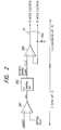
- Fig. 1 illustrates an embodiment 1 of the present invention.
- the STM of the present embodiment is to detect the tunnelling current generated when a bias voltage is applied between an observed specimen and a probe opposed thereto.
- an observed specimen 1 and a probe 2 positioned close thereto.
- the probe 2 is mounted on an unrepresented Z-fine movement drive mechanism such as a laminated piezoelectric element, and constitutes a cantilever actuator drivable in the Z-direction by the electrostatic force, under the application of a voltage.
- a pointed conductive tip 3 At the end of the cantilever there is formed a pointed conductive tip 3, for detecting the tunnelling current flowing between the tip and the observed specimen.
- the above-mentioned probe is constructed in the following manner.
- the probe 2 is constructed as a cantilever drivable by the electrostatic force.
- the cantilever probe is formed on a support member 9, across an insulating layer 10, and the probe 2 moves in the Z-direction by the application of an actuator drive signal between drive electrodes 11 formed on the support member 9 and the probe 2.
- the Z-fine drive mechanism is activated under the application of a bias voltage by a bias circuit 4 between the probe 2 and the specimen 1 to bring the probe so close to the specimen as to generate a tunnelling current, and the probe 2 is servo controlled as to maintain a constant distance between the probe and the specimen.
- tunnelling current Jt varying by the small irregularities on the specimen surface.
- This current is fetched in a control circuit 7 and is processed in synchronization with xy scanning signals to obtain an STM image.
- the STM image is subjected to image processing, such as two-dimensional FFT, to obtain a tunnelling current image and a topographic image (distance control signal image), which are supplied to a display 8.
- image processing such as two-dimensional FFT
- the location of observation may be changed by moving the specimen in the X- and Y-directions by an unrepresented XY coarse movement drive mechanism, so as to move the probe 2 to a desired area of observation.
- the control circuit effects servo operation, at the observation of the specimen, so as to maintain a constant distance between the probe and the specimen.
- the tunnelling current Jt detected by the probe 2 is converted into a voltage by a current-voltage conversion circuit 12.
- the output Vt of the current-voltage conversion circuit 12 is supplied to a logarithmic conversion circuit 13, of which output Log(Vt) is supplied to a Z-servo circuit 14.
- the Z-servo circuit 14 releases a distance control signal 15 so as to maintain a constant distance between the probe and the specimen.
- a V-Q conversion circuit 16 converts the distance output signal 15 into an actuator control signal 17, for supply to an electrostatic drive electrode for driving the probe in the z-direction.
- the probe and the specimen are maintained at a constant distance by the electrostatic drive of the actuator by this control signal.
- the Z-servo circuit 14 and the V-Q conversion circuit 16 featuring the present invention.
- the output Log(Vt) of the logarithmic conversion circuit 13 is supplied to the Z-servo circuit 14.
- the output Log(Vt) is proportional to the distance signal between the probe and the medium.
- the Z-servo circuit 14 releases the distance control signal 15 so as to maintain this distance constant.
- the output Log(Vt) is supplied to a subtractor 201, and is converted to an error signal err by the subtraction of a preset value ZO.
- the error signal err enters a PI control circuit 202 and is subjected to proportional integration therein to generate the distance control signal 15 (:V).
- This distance control signal 15 is converted by the V-Q conversion circuit 16, in Fig. 1, into the actuator control signal 17, which is a charge control signal and is applied between the drive electrodes for generating the electrostatic force.
- the voltage-charge (V-Q) conversion circuit 16 therefor will be explained in the following.
- the V-Q conversion circuit converts the input voltage signal into a charge signal which controls the charge amount accumulated in a capacitor formed between the electrostatic drive electrodes, thereby controlling the electrostatic actuator.
- the V-Q conversion circuit is provided with a small capacitor 204, for detecting the leak current, serially with the capacitor formed between the electrostatically driven electrodes.
- the actuator for driving the probe in the Z-direction is composed of a cantilever actuator drivable in the Z-direction by the electrostatic force.
- the Z-displacement of the electrostatically driven cantilever is defined in the following manner, for a cantilever with a width W, a length L and a thickness t, and for a charge amount Q between the drive electrodes.
- control method for maintaining a constant charge amount between the electrostatic drive electrodes enables constant feedback control between the probe and the medium, avoiding uncontrollable situation of the actuator, thereby allowing to stably obtain the STM image.
- the charge amount between the drive electrodes of the actuator is monitored and controlled by the potential of a capacitor connected serially to an equivalent capacitor formed between the drive electrodes, but it is also possible, for example, to calculate the charge amount in the equivalent capacitor formed between the drive electrodes, by means of an integrating circuit, and to effect control based on thus calculated charge amount.
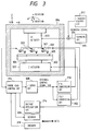
- Fig. 3 is a block diagram of an information recording/reproducing apparatus utilizing multiple probes, constituting a second embodiment of the present invention.
- the recording/reproducing apparatus of the present embodiment effects information exchange by plural probes for detecting the tunnelling current generated under the application of a bias voltage between a recording medium and a probe opposed thereto.
- a multi-probe head 301, bearing 16 probes 300, is positioned close to a recording medium 302.
- the multi-probe head 301 is mounted, through an XY actuator 303 constituting a drive mechanism in the X- and Y-directions, on a support member 304.
- the recording medium 302 bears a tracking pattern 305 (a recessed groove pattern or a pattern of a different surfacial electronic state) and is placed on a base member 306, which is mounted, through a Z-actuator 307 capable of displacement in the Z-direction and rotations in the ⁇ - and ⁇ -directions, on the support member 304.
- the multi-probe head 301 is composed of silicon, bearing 16 probes in a 4 ⁇ 4 matrix array.
- Each probe is constructed as a torsion-bar actuator, in which a flat plate portion formed on a beam supported at both ends is elctrostatically driven, utilizing the torsion elasticity of the beam supported at both ends.
- this torsion-bar actuator allows independent selection of the bending elasticity of the lever and the torsion elasticity of the beam, allowing larger freedom in the designing of ridigity and resonance frequency. Also a displacement in the Z-direction is induced by the application of a voltage between drive electrodes 320. (The details of the torsion-bar actuator and the method of preparation thereof will be explained later.)
- a pointed conductive tip At the end of the cantilever, there is formed a pointed conductive tip, for detecting the tunnelling current between the tip and the opposed recording medium.
- the probes 300 of the multi-probe head 301 are brought so close to the opposed recording medium 302 as to induce tunnelling currents therebetween.
- the tunnelling current signal from each probe is supplied through a probe head control circuit 311 to a Z-servo circuit 308, which in response generates a distance control signal 309 for maintaining a constant distance between each probe and the opposed recording medium.
- the distance control signal 309 for independently driving each probe in the Z-direction, is supplied through a V-Q conversion circuit 310 to the electrodes of each actuator.
- a tilt correction circuit 312 corrects the tilt between the multi-probe head 301 and the recording medium 302.
- a scanning circuit 315 causes, according to an XY scanning signal 316 XY scanning motions of the probe head 301 relative to the recording medium 302.
- a tracking control circuit 317 detects the edge position of the tracking pattern 305, from the variation in the tunnelling current of each probe 300 and corrects, by the XY actuator 303, the positional aberration between the tracking pattern 305 and the multi-probe head 301. In this state a voltage application circuit 314 modulates the tunnelling current between each probe and the recording medium, thereby forming recording bits on the recording medium.
- Fig. 4 is a perspective view showing the structure of the torsion-bar actuator employed in the present embodiment.
- a mechanically movable part is formed, across a gap 404, on a substrate 401 bearing a fixed electrode 403 on an insulating layer 402.
- the mechanically movable part is composed of a beam 409 for rotational support, supported at both ends, and a probe 408, and is supported by support portions 410.
- the probe of the present embodiment is driven in the following manner.
- the rear end portion of the probe is attracted toward the fixed electrode 403.
- the entire probe 408 rotates about the axis of the beam 409 supported at both ends, whereby the tip 412 at the front end of the probe 408 moves closer to the opposed recording medium.
- a silicon nitride film was formed with a thickness of 3000 ⁇ by low pressure CVD (LPCVD) to constitute the insulating layer 402.
- photoresist was coated and patterned, and Ti and Pt were deposited in succession, by sputtering, with respective thicknesses of 50 ⁇ and 2000 ⁇ . Subsequently the photoresist was eliminated to obtain the fixed electrode 403.
- silicon oxide was deposited by sputtering with a thickness of 10000 ⁇ .
- a silicon nitride film 502 was deposited with a thickness of 1000 ⁇ by low pressure CVD (LPCVD) (Fig. 5(d)).
- the silicon nitride film was photolithographically etched into the form shown in Fig. 5(e), thereby exposing the surface of the second substrate.
- the second substrate 501 was subjected to anisotropic crystal etching with aqueous solution of potassium hydroxide heated to 100°C, thereby forming an inverse pyramidal recess 503, constituting a mold for the tip (Fig. 5(e)).
- the tip 412 was pressed onto the substrate 401, and peeled off from the interface of the second substrate 501, thereby obtaining the information input/output tip 412 (Fig. 5(g)).
- the etching of the second substrate 501 may be made not only by the anisotropic crystal etching for example of monocrystalline silicon or GaAs semiconductor, but also by the isotropic etching if there can be obtained a transferrable shape.
- a protective layer 502, at the etching of the second substrate 501, may be composed of any substance that can withstands the solution employed in the above-mentioned etching.
- the probe 408 formed on the first substrate 408 and the tip 412 formed on the second substrate 501 may be bonded, for example by metal-metal junction or anodic junction.
- the sacrifice layer 405 composed of zinc oxide was etched off with aqueous solution of acetic acid, thereby forming the gap 404 between the probe 408 and the fixed electrode 403.
- Such torsion-bar probes were prepared in a 4 ⁇ 4 matrix array, and a tunnelling current detecting amplifier was prepared by an IC process, in the vicinity of each torsion-bar probe on the Si wafer, thereby constituting the multi-probe head 301.
- stripe-shaped tracking patterns are formed for example by a semiconductor process.
- the recording medium 302 was composed of a material showing memory effect to the voltage-current switching.
- the substrate electrode was composed of an epitaxially grown Au surface, formed on a flat substrate such as glass or mica.
- the tracking grooves were formed on the substrate electrode, and the recording medium thereon was formed by two superposed Langmuir-Brodget monomolecular films of squarilium-bis-6-octyl-azulene (SOAZ).
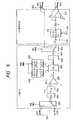
- the control circuit of the present embodiment effects distance control between the medium and the opposed plural probes for detecting the tunnelling currents.
- a digital servo system for converting the tunnelling current signal from each probe into a digital signal and, based on these signals, generating Z-control signals for controlling the probes in succession, according to the timing of a probe head control circuit 311.
- the tunnelling current signals from the multiple probes 1 - n are supplied to a selection circuit 602.
- the selection circuit 602 selects, according to the control timing, one of the multiple probes 601, for example an n-th probe (In).
- the tunnelling current signal detected from thus selected n-th probe is converted into a voltage, then is A/D converted in an A/D converter 603 (as indicated by In(t), wherein t indicates the sampling time).
- digitized tunnelling current signal is subjected to a linear conversion, with respect to the probe-medium distance, by the logarithmic conversion circuit 604 (LogIn(t) in Fig. 6).
- the output of the logarithmic conversion circuit 604 is supplied to a subtracting comparator 605, for effecting comparison with a set value ZO of the servo circuit, thereby generating an error signal En(t).
- a PI control circuit 606 generates a distance control signal Un(t) so as to bring the error signal to zero.
- the PI control circuit 606 generates a new distance control signal Un(t) at a time (t), based on the distance control signal and the corrected error signal data at a sampling time (t - 1) and corrected error signal En(t) at the sampling time (t), stored in memories 607, 608, and simultaneously renews the data stored in the memories 607, 608.
- the distance control signal Un(t) is again converted into an analog distance control signal 309 (Un) by a D/A converter 609, and is further converted by a V-Q conversion circuit 310 into a charge control signal, which is applied between the drive electrodes of the electrostatic actuator.
- the control circuit 311 effects Z-control on all the probes by switching the selected probe with the selection circuits 602, 613.
- the charge between the drive electrodes is controlled in the control of the electrostatically driven actuator, as in the foregoing first embodiment.
- the present embodiment however employs an AC drive signal and effects the probe position control based on the charge amount, obtained by integration in time of the detected current, generated by the above-mentioned AC drive signal.
- a V-Q conversion circuit is composed of an AC voltage generator 611, an amplitude modulation circuit 612 capable of amplitude control with variation in the frequency, and an integration circuit 614.
- the integrating circuit 614 is composed of an operational amplifier, a resistor R and the equivalent capacitor c formed between the drive electrodes, and controls the current flowing into the equivalent capacitor.
- the capacitor 610 is a sample-hold (S/H) capacitor, for storing the control signal Un for determining the amplitude of the oscillator circuit, and holds the distance control signal Un from the Z-servo circuit at the signal switching.
- S/H sample-hold
- Ave (Un/ ⁇ •R) 2 /2
- the use of the AC drive signal enables control of the electrostatic actuator, without generation of the potential, averaged in time, between the drive electrodes.
- the mechanical parameters of the torsion-bar probe were estimated as follows.
- a bias voltage of 0.1 V was applied by the voltage application circuit 414, between each probe 300 and the recording medium, and both were brought to a small distance providing a constant tunnelling current (1 nA).
- Each probe was independently driven in the Z-direction by the Z-servo circuit 308, with feedback control so as to obtain a constant current of 1 nA.
- the tilt correction circuit 312 generate an ⁇ -rotation signal and a ⁇ -rotation signal for correcting the tilt between the multi-probe head 301 and the recording medium and apply those to the Z-actuator 307.
- the probe was brought to a desired position on the recording medium 302, and the bias voltage was modulated to apply a pulsed voltage of 6 V between the probe 300 and the recording medium, whereby a record bit of a size of 10 nm ⁇ was formed, allowing a current of ca. 0.1 ⁇ A to flow, and, in a scanning operation after the application of the pulsed voltage, this state was found to be retained.
- bit of lower resistance state was defined as "1”
- the higher resistance state was defined as "0”
- binary recording and reproduction were conducted by encoding data with an encoder 318 and decoding the reproduced binary data with a decoder 319.
- the electrostatic actuator is driven by an AC voltage and the charge amount control is made by the amplitude of the AC voltage, but such charge amount control can also be achieved by the variation in the driving frequency or in the current limiting resistor, according to the equation (9).
- tunnelling current as the physical interaction, but there may also be utilized other physical interactions such as interatomic force, magnetic force or evanescent light.
Landscapes
- Chemical & Material Sciences (AREA)
- General Physics & Mathematics (AREA)
- General Health & Medical Sciences (AREA)
- Physics & Mathematics (AREA)
- Nuclear Medicine, Radiotherapy & Molecular Imaging (AREA)
- Radiology & Medical Imaging (AREA)
- Health & Medical Sciences (AREA)
- Engineering & Computer Science (AREA)
- Nanotechnology (AREA)
- Analytical Chemistry (AREA)
- Crystallography & Structural Chemistry (AREA)
- Measurement Of Length, Angles, Or The Like Using Electric Or Magnetic Means (AREA)
- Micromachines (AREA)
Applications Claiming Priority (3)
| Application Number | Priority Date | Filing Date | Title |
|---|---|---|---|
| JP2121595 | 1995-01-13 | ||
| JP02121595A JP3610108B2 (ja) | 1995-01-13 | 1995-01-13 | 情報処理装置 |
| JP21215/95 | 1995-01-13 |
Publications (3)
| Publication Number | Publication Date |
|---|---|
| EP0722077A2 true EP0722077A2 (fr) | 1996-07-17 |
| EP0722077A3 EP0722077A3 (fr) | 1997-01-29 |
| EP0722077B1 EP0722077B1 (fr) | 2002-07-24 |
Family
ID=12048792
Family Applications (1)
| Application Number | Title | Priority Date | Filing Date |
|---|---|---|---|
| EP96100370A Expired - Lifetime EP0722077B1 (fr) | 1995-01-13 | 1996-01-11 | Appareil de traitement d'informations avec contrôle de la position d'une sonde par forces électrostatiques |
Country Status (4)
| Country | Link |
|---|---|
| US (1) | US5793040A (fr) |
| EP (1) | EP0722077B1 (fr) |
| JP (1) | JP3610108B2 (fr) |
| DE (1) | DE69622442T2 (fr) |
Families Citing this family (8)
| Publication number | Priority date | Publication date | Assignee | Title |
|---|---|---|---|---|
| US6366340B1 (en) * | 1995-08-18 | 2002-04-02 | Hitachi, Ltd. | Electron exposure apparatus |
| US6473361B1 (en) * | 2000-11-10 | 2002-10-29 | Xerox Corporation | Electromechanical memory cell |
| KR100499125B1 (ko) * | 2002-04-25 | 2005-07-04 | 삼성전자주식회사 | 커패시턴스 변화를 이용하는 정보 재생 장치 및 방법 |
| US7155964B2 (en) * | 2002-07-02 | 2007-01-02 | Veeco Instruments Inc. | Method and apparatus for measuring electrical properties in torsional resonance mode |
| US7349236B2 (en) * | 2005-06-24 | 2008-03-25 | Xerox Corporation | Electromechanical memory cell with torsional movement |
| JP4814705B2 (ja) * | 2005-10-13 | 2011-11-16 | パナソニック株式会社 | 半導体集積回路装置及び電子装置 |
| WO2007114355A1 (fr) * | 2006-03-31 | 2007-10-11 | Pioneer Corporation | Dispositif de stockage d'informations utilisant une sonde |
| US7486403B2 (en) * | 2006-07-20 | 2009-02-03 | Canon Kabushiki Kaisha | Droplet shape measuring method and apparatus |
Family Cites Families (24)
| Publication number | Priority date | Publication date | Assignee | Title |
|---|---|---|---|---|
| JPS6180536A (ja) * | 1984-09-14 | 1986-04-24 | ゼロツクス コーポレーシヨン | 原子規模密度情報記緑および読出し装置並びに方法 |
| JPS61154984A (ja) * | 1984-12-28 | 1986-07-14 | Yoshida Kogyo Kk <Ykk> | 合成樹脂成形品の染色方法とその装置 |
| DE3679319D1 (de) * | 1986-05-27 | 1991-06-20 | Ibm | Speichereinheit mit direktem zugriff. |
| US4922756A (en) * | 1988-06-20 | 1990-05-08 | Triton Technologies, Inc. | Micro-machined accelerometer |
| EP0262253A1 (fr) * | 1986-10-03 | 1988-04-06 | International Business Machines Corporation | Dispositif micromécanique détecteur de forces atomiques |
| JP2556492B2 (ja) * | 1986-12-24 | 1996-11-20 | キヤノン株式会社 | 再生装置及び再生法 |
| JP2556491B2 (ja) * | 1986-12-24 | 1996-11-20 | キヤノン株式会社 | 記録装置及び記録法 |
| FR2616435B1 (fr) * | 1987-06-15 | 1989-10-06 | Atochem | Procede de fabrication de polybutadiene hydroxyle |
| JP2557964B2 (ja) * | 1988-01-22 | 1996-11-27 | インターナシヨナル・ビジネス・マシーンズ・コーポレイーシヨン | データ記憶装置 |
| US5220555A (en) * | 1988-09-30 | 1993-06-15 | Canon Kabushiki Kaisha | Scanning tunnel-current-detecting device and method for detecting tunnel current and scanning tunnelling microscope and recording/reproducing device using thereof |
| JP2896794B2 (ja) * | 1988-09-30 | 1999-05-31 | キヤノン株式会社 | 走査型トンネル電流検出装置,走査型トンネル顕微鏡,及び記録再生装置 |
| DE3850968T2 (de) * | 1988-10-14 | 1995-03-16 | Ibm | Abstandsgesteuerter Tunneleffektwandler und den Wandler verwendende Speichereinheit mit direktem Zugriff. |
| JP2775464B2 (ja) * | 1989-04-27 | 1998-07-16 | キヤノン株式会社 | 位置検出装置 |
| US5132533A (en) * | 1989-12-08 | 1992-07-21 | Canon Kabushiki Kaisha | Method for forming probe and apparatus therefor |
| JP2901080B2 (ja) * | 1989-12-14 | 1999-06-02 | キヤノン株式会社 | 光電変換装置 |
| US5144128A (en) * | 1990-02-05 | 1992-09-01 | Hitachi, Ltd. | Surface microscope and surface microscopy |
| US5283437A (en) * | 1990-12-21 | 1994-02-01 | International Business Machines Corporation | Pneumatically and electrostatically driven scanning tunneling microscope |
| JP2930447B2 (ja) * | 1991-05-15 | 1999-08-03 | キヤノン株式会社 | 情報処理装置 |
| JP2994505B2 (ja) * | 1991-10-04 | 1999-12-27 | キヤノン株式会社 | 情報再生装置 |
| JP3060142B2 (ja) * | 1992-06-26 | 2000-07-10 | キヤノン株式会社 | カンチレバー型変位素子の駆動方法、走査型トンネル顕微鏡、情報処理装置、及びカンチレバー型変位素子 |
| JP3402661B2 (ja) * | 1992-07-06 | 2003-05-06 | キヤノン株式会社 | カンチレバー型プローブ、及びこれを用いた情報処理装置 |
| US5338932A (en) * | 1993-01-04 | 1994-08-16 | Motorola, Inc. | Method and apparatus for measuring the topography of a semiconductor device |
| JP2704601B2 (ja) * | 1993-04-12 | 1998-01-26 | セイコーインスツルメンツ株式会社 | 走査型近視野原子間力顕微鏡、及びその顕微鏡に使用されるプローブ、及びそのプローブの製造方法 |
| JP3016060B2 (ja) * | 1993-04-28 | 2000-03-06 | 本田技研工業株式会社 | 防振マウント装置 |
-
1995
- 1995-01-13 JP JP02121595A patent/JP3610108B2/ja not_active Expired - Fee Related
-
1996
- 1996-01-11 EP EP96100370A patent/EP0722077B1/fr not_active Expired - Lifetime
- 1996-01-11 DE DE69622442T patent/DE69622442T2/de not_active Expired - Fee Related
- 1996-01-16 US US08/586,090 patent/US5793040A/en not_active Expired - Lifetime
Also Published As
| Publication number | Publication date |
|---|---|
| JPH08194975A (ja) | 1996-07-30 |
| DE69622442T2 (de) | 2002-12-12 |
| EP0722077A3 (fr) | 1997-01-29 |
| DE69622442D1 (de) | 2002-08-29 |
| JP3610108B2 (ja) | 2005-01-12 |
| EP0722077B1 (fr) | 2002-07-24 |
| US5793040A (en) | 1998-08-11 |
Similar Documents
| Publication | Publication Date | Title |
|---|---|---|
| Kado et al. | Nanometer‐scale recording on chalcogenide films with an atomic force microscope | |
| EP0523676B1 (fr) | Appareil d'enregistrement/reproduction pour enregistrer ou reproduire de l'information sur/d'un support d'enregistrement d'information au moyen d'une électrode-sonde. | |
| JP3246987B2 (ja) | マルチプローブ制御回路を具備する情報処理装置 | |
| US5481527A (en) | Information processing apparatus with ferroelectric rewritable recording medium | |
| US5506829A (en) | Cantilever probe and apparatus using the same | |
| US6252226B1 (en) | Nanometer scale data storage device and associated positioning system | |
| US5574279A (en) | Probe with torsion lever structure, and scanning probe microscope and record/reproducing apparatus utilizing the same | |
| WO1997004449A1 (fr) | Dispositif de stockage de donnees a l'echelle nanometrique et systeme de positionnement associe | |
| US5371728A (en) | Information recording/reproducing apparatus using probe | |
| EP0431623B1 (fr) | Méthode et appareil de façonnement d'une sonde | |
| EP0537642B1 (fr) | Appareil de traitement d'information à mécanisme d'alignement de piste | |
| US5793040A (en) | Information processing aparatus effecting probe position control with electrostatic force | |
| US5751686A (en) | Scanning probe tip covered with an electrical resistance to limit recording/reproducing current | |
| US5978326A (en) | Information processing apparatus using an offset signal to control the position of a probe | |
| JPH07260802A (ja) | 微小変位素子、光偏向器、走査型プローブ顕微鏡、および情報処理装置 | |
| JP3203433B2 (ja) | 変位素子、及びこれを用いた検出素子、及びこの検出素子を用いた走査型トンネル顕微鏡、情報処理装置 | |
| JP3226424B2 (ja) | 走査型プローブ顕微鏡ならびに該顕微鏡を用いた加工装置および情報処理装置 | |
| JPH05342648A (ja) | 情報読取り及び/又は入力装置 | |
| CA2031733C (fr) | Methode et appareil pour fabriquer une sonde | |
| JP3118654B2 (ja) | 情報処理装置及び走査型トンネル電子顕微鏡 | |
| JPH07110969A (ja) | 面合わせ方法,位置制御機構および該機構を有する情報処理装置 | |
| JPH09196929A (ja) | 表面観察装置と表面観察方法、記録装置と記録方法、及び再生装置と再生方法 | |
| JP3093065B2 (ja) | 記録再生方法および記録再生装置 | |
| JPH08304422A (ja) | 情報処理装置および情報処理方法 | |
| JP2934057B2 (ja) | プローブユニット及びこれを使用する情報記録及び/又は再生装置 |
Legal Events
| Date | Code | Title | Description |
|---|---|---|---|
| PUAI | Public reference made under article 153(3) epc to a published international application that has entered the european phase |
Free format text: ORIGINAL CODE: 0009012 |
|
| AK | Designated contracting states |
Kind code of ref document: A2 Designated state(s): DE FR GB |
|
| PUAL | Search report despatched |
Free format text: ORIGINAL CODE: 0009013 |
|
| AK | Designated contracting states |
Kind code of ref document: A3 Designated state(s): DE FR GB |
|
| 17P | Request for examination filed |
Effective date: 19970729 |
|
| 17Q | First examination report despatched |
Effective date: 19991027 |
|
| RTI1 | Title (correction) |
Free format text: INFORMATION PROCESSING APPARATUS EFFECTING PROBE POSITION CONTROL WITH ELECTROSTATIC FORCES |
|
| GRAG | Despatch of communication of intention to grant |
Free format text: ORIGINAL CODE: EPIDOS AGRA |
|
| GRAG | Despatch of communication of intention to grant |
Free format text: ORIGINAL CODE: EPIDOS AGRA |
|
| GRAH | Despatch of communication of intention to grant a patent |
Free format text: ORIGINAL CODE: EPIDOS IGRA |
|
| GRAH | Despatch of communication of intention to grant a patent |
Free format text: ORIGINAL CODE: EPIDOS IGRA |
|
| GRAA | (expected) grant |
Free format text: ORIGINAL CODE: 0009210 |
|
| AK | Designated contracting states |
Kind code of ref document: B1 Designated state(s): DE FR GB |
|
| PG25 | Lapsed in a contracting state [announced via postgrant information from national office to epo] |
Ref country code: FR Free format text: LAPSE BECAUSE OF FAILURE TO SUBMIT A TRANSLATION OF THE DESCRIPTION OR TO PAY THE FEE WITHIN THE PRESCRIBED TIME-LIMIT Effective date: 20020724 |
|
| REG | Reference to a national code |
Ref country code: GB Ref legal event code: FG4D |
|
| REF | Corresponds to: |
Ref document number: 69622442 Country of ref document: DE Date of ref document: 20020829 |
|
| EN | Fr: translation not filed | ||
| PLBE | No opposition filed within time limit |
Free format text: ORIGINAL CODE: 0009261 |
|
| STAA | Information on the status of an ep patent application or granted ep patent |
Free format text: STATUS: NO OPPOSITION FILED WITHIN TIME LIMIT |
|
| 26N | No opposition filed |
Effective date: 20030425 |
|
| PGFP | Annual fee paid to national office [announced via postgrant information from national office to epo] |
Ref country code: GB Payment date: 20050105 Year of fee payment: 10 |
|
| PGFP | Annual fee paid to national office [announced via postgrant information from national office to epo] |
Ref country code: DE Payment date: 20050106 Year of fee payment: 10 |
|
| PG25 | Lapsed in a contracting state [announced via postgrant information from national office to epo] |
Ref country code: GB Free format text: LAPSE BECAUSE OF NON-PAYMENT OF DUE FEES Effective date: 20060111 |
|
| PG25 | Lapsed in a contracting state [announced via postgrant information from national office to epo] |
Ref country code: DE Free format text: LAPSE BECAUSE OF NON-PAYMENT OF DUE FEES Effective date: 20060801 |
|
| GBPC | Gb: european patent ceased through non-payment of renewal fee |
Effective date: 20060111 |