EP0722632B1 - Etage de repli pour un convertisseur analogique-numerique a repli - Google Patents
Etage de repli pour un convertisseur analogique-numerique a repli Download PDFInfo
- Publication number
- EP0722632B1 EP0722632B1 EP95921101A EP95921101A EP0722632B1 EP 0722632 B1 EP0722632 B1 EP 0722632B1 EP 95921101 A EP95921101 A EP 95921101A EP 95921101 A EP95921101 A EP 95921101A EP 0722632 B1 EP0722632 B1 EP 0722632B1
- Authority
- EP
- European Patent Office
- Prior art keywords
- coupled
- folding
- transistor
- node
- output
- Prior art date
- Legal status (The legal status is an assumption and is not a legal conclusion. Google has not performed a legal analysis and makes no representation as to the accuracy of the status listed.)
- Expired - Lifetime
Links
- 230000001174 ascending effect Effects 0.000 claims description 3
- 230000003071 parasitic effect Effects 0.000 description 11
- 230000000694 effects Effects 0.000 description 6
- 238000010586 diagram Methods 0.000 description 4
- 238000006243 chemical reaction Methods 0.000 description 3
- 230000014509 gene expression Effects 0.000 description 3
- 238000000034 method Methods 0.000 description 3
- 239000011800 void material Substances 0.000 description 3
- 230000003321 amplification Effects 0.000 description 2
- 238000010276 construction Methods 0.000 description 2
- 238000003199 nucleic acid amplification method Methods 0.000 description 2
- 238000004458 analytical method Methods 0.000 description 1
- 230000000295 complement effect Effects 0.000 description 1
- 230000007423 decrease Effects 0.000 description 1
- 230000003247 decreasing effect Effects 0.000 description 1
- 230000005284 excitation Effects 0.000 description 1
- 230000003252 repetitive effect Effects 0.000 description 1
Images


Classifications
-
- H—ELECTRICITY
- H03—ELECTRONIC CIRCUITRY
- H03M—CODING; DECODING; CODE CONVERSION IN GENERAL
- H03M1/00—Analogue/digital conversion; Digital/analogue conversion
- H03M1/12—Analogue/digital converters
- H03M1/20—Increasing resolution using an n bit system to obtain n + m bits
- H03M1/202—Increasing resolution using an n bit system to obtain n + m bits by interpolation
- H03M1/203—Increasing resolution using an n bit system to obtain n + m bits by interpolation using an analogue interpolation circuit
- H03M1/204—Increasing resolution using an n bit system to obtain n + m bits by interpolation using an analogue interpolation circuit in which one or more virtual intermediate reference signals are generated between adjacent original reference signals, e.g. by connecting pre-amplifier outputs to multiple comparators
- H03M1/205—Increasing resolution using an n bit system to obtain n + m bits by interpolation using an analogue interpolation circuit in which one or more virtual intermediate reference signals are generated between adjacent original reference signals, e.g. by connecting pre-amplifier outputs to multiple comparators using resistor strings for redistribution of the original reference signals or signals derived therefrom
-
- H—ELECTRICITY
- H03—ELECTRONIC CIRCUITRY
- H03M—CODING; DECODING; CODE CONVERSION IN GENERAL
- H03M1/00—Analogue/digital conversion; Digital/analogue conversion
- H03M1/12—Analogue/digital converters
- H03M1/14—Conversion in steps with each step involving the same or a different conversion means and delivering more than one bit
- H03M1/141—Conversion in steps with each step involving the same or a different conversion means and delivering more than one bit in which at least one step is of the folding type; Folding stages therefore
-
- H—ELECTRICITY
- H03—ELECTRONIC CIRCUITRY
- H03M—CODING; DECODING; CODE CONVERSION IN GENERAL
- H03M1/00—Analogue/digital conversion; Digital/analogue conversion
- H03M1/06—Continuously compensating for, or preventing, undesired influence of physical parameters
- H03M1/0602—Continuously compensating for, or preventing, undesired influence of physical parameters of deviations from the desired transfer characteristic
- H03M1/0604—Continuously compensating for, or preventing, undesired influence of physical parameters of deviations from the desired transfer characteristic at one point, i.e. by adjusting a single reference value, e.g. bias or gain error
- H03M1/0607—Offset or drift compensation
Definitions
- the invention relates to a folding stage for a folding analog-to-digital converter, the folding stage comprising:
- Such a folding stage is known from United States Patent No. 4,386,339. Folding stages are commonly used in analog-to-digital (A/D) converters.
- Full flash converters have a relatively simple architecture.
- To convert an analog input voltage into an N-bit digital output code, a full flash converter normally employs 2 N -1 input comparators for comparing the input voltage with 2 N -1 corresponding reference voltages.
- the principal disadvantage of the full flash converter is the high component count due to the large number of input comparators.
- the folding technique is one of the schemes for reducing component count.
- Folding architectures have been successfully implemented in very high speed bipolar A/D converters. See R. van de Grift et al., "An 8-bit Video ADC Incorporating Folding and Interpolating Techniques", IEEE Journal of Solid-State Circuits, Vol. SC-22, No. 6, December 1987, pp 944-953. Also see R. van de Plassche et al., "An 8-bit 100-MHz Full-Nyquist Analog-to Digital Converter", IEEE Journal of Solid-State Circuits, Vol. 23, No. 6, December 1988, pp 1334-1344. The basic principles of the folding architecture are extensively explained in these references.
- a folding A/D converter comprises a number of folding stages, each comprising a set of differential pairs responding to the input voltage and a corresponding set of reference voltages.
- the outputs of the differential pairs are combined in such a way as to generate one or more single ended folding signals or pairs of complementary folding signals having a repetitive rounded triangular or sine wave shape as a function of the input voltage.
- the folding signals of the folding stages are supplied to respective one's of a group of sample latches for converting the folding signals to a group of least significant bits of the digital output code.
- the most significant bits are supplied by a group of coarse comparators which operate on the input voltage along a separate channel. In this way the number of latches can be reduced considerably.
- the number of latches is reduced by the number of times the input signal is folded by the folding stages.
- each latch requires its own folding signal and each folding stage requires as many differential pairs as the number of times the signal has been folded.
- the more efficient use of the latches is therefore offset by an increasing number of differential pairs in the folding stages.
- the number of folding stages can be reduced by interpolating between the folding signals of the folding stages to generate additional folding signals without the need for more folding stages. In this way the interpolation reduces the number of folding stages by the interpolation factor.
- a combined folding and interpolating architecture results in a compact low-power A/D converter.
- the folding technique is also useful in other A/D architectures.
- United States Patent No. 4,386,339 a direct flash A/D converter is disclosed having independent parallel A/D converters for each bit.
- Each independent bit-encoder has a folding stage coupled to a single comparator which provides a bit of directly encoded compact binary output. In this way conversion from thermometer code to binary code is not needed.
- a folding stage thus can be used in several distinct A/D converter architectures.
- the folding system implies that the frequency of the folding signal will be a multiple of the frequency of the input signal to be folded.
- the folding stage as specified in the opening paragraph is characterized in that the folding stage further comprises a dummy structure comprising a first current source, a first dummy transistor having a control electrode coupled to the input terminal, a first main electrode connected to the first current source and a second main electrode coupled to one of the first and second summing nodes, a second current source, and a second dummy transistor having a control electrode coupled to a bias voltage terminal, a first main electrode connected to the second current source and a second main electrode coupled to the other of the first and second summing nodes.
- a dummy structure comprising a first current source, a first dummy transistor having a control electrode coupled to the input terminal, a first main electrode connected to the first current source and a second main electrode coupled to one of the first and second summing nodes, a second current source, and a second dummy transistor having a control electrode coupled to a bias voltage terminal, a first main electrode connected to the second current source and a second main electrode coupled to the other
- the dummy structure reduces the capacitive error current in the differential output current which flows in the summing nodes of the folding stage by providing cancelling currents to the summing nodes.
- a folding stage In a folding stage many transistors are connected to the summing nodes. Parasitic capacitances of the transistors of the differential pairs may also deteriorate the output currents in the summing nodes. The currents through the parasitic capacitances can be relatively large compared to the differential current swing and may reduce the desired accuracy. It is therefore advantageous to keep the voltage swing at the summing nodes as small as possible to prevent unacceptable capacitive currents through the parasitic capacitances.
- a folding stage according to the invention may be further characterised in that the folding stage further comprises:
- the output voltage at the first output node is proportional to the resistance R of the first resistor.
- the input impedance of the transconductance stage is equal to 1/g m , g m being the transconductance of the transconductance stage.
- the output impedance of the transconductance stage is also 1/g m .
- a large transconductance provides a low input impedance to reduce the voltage swing and thus the capacitive currents.
- a large transconductance further provides a low output impedance. This allows for a large resistance R to provide a large output voltage at the output node.
- the output voltage and the output impedance can be designed separately by selecting suitable values for the resistance R of the first resistor and for the transconductance g m of the transconductance stage. This makes connection possible to a low impedance interpolation network. A low impedance level of the interpolation network is less sensitive to parasitic capacitances and thus allows higher speed.
- the two summing nodes of the folding stage need a bias current. Mismatch between the two bias currents causes offset in the output currents of the folding stage. This offset results in non-linearity errors of a folding A/D converter and should be avoided as much as possible.
- the folding stage further comprises a first bias current source coupled to the first output node for providing a first bias current to the first summing node via the first resistor.
- the output voltage of the folding stage can be single ended.
- a folding stage having a differential output is characterized in that - the folding stage further comprises a second output node;
- differential signals For high speed applications the generation of differential signals is preferred, since it greatly improves the reliability and robustness of a folding AID converter under noisy conditions corresponding to a digital environment.
- the transconductance stage may be implemented in any suitable way.
- a simple differential transconductance stage comprising only a few components is characterized in that the transconductance stage comprises a first transistor and a second transistor having first main electrodes coupled to a common current source, having second main electrodes coupled to the first output node and the second output node, respectively, and having control electrodes coupled to the first summing node and the second summing node, respectively.
- This differential transconductance stage may be further characterized in that the transconductance stage further comprises a third resistor connected between the first output node and the second summing node and a fourth resistor connected between the second output node and the first summing node.
- the third and fourth resistors are cross-coupled and provide a lower DC voltage drop between the summing nodes and the output nodes, while maintaining the same differential signal amplification.
- common-mode signals bias currents
- the first and third resistors are seen in parallel; the same holds for the second and fourth resistors.
- differential mode signal currents
- the first and third resistors are seen in parallel with a minus sign for the third resistor, thereby effectively increasing the parallel resistance; the same holds for the second and fourth resistors.
- the folding stage may be further characterized in that in at least two of the plurality of differentially coupled transistor pairs the control electrode of the second transistor is coupled to a reference terminal supplying a reference voltage which lies outside the voltage range of the input voltage to be folded.
- the two differential pairs generate void zerocrossings at the end of the input voltage range.
- all differential pairs are equally influenced by adjacent pairs.
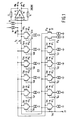
- Figure 1 shows an eight times folding stage FB with unipolar MOS transistors.
- bipolar transistors can be used as well.
- the control electrode, first main electrode and second main electrode correspond to the gate, source and drain, respectively, of an unipolar transistor and to the base, emitter and collector, respectively, of a bipolar transistor.
- Eight times folding means that eight zerocrossings are generated when the input voltage traverses its specified input voltage range.
- Figure 2 shows the functioning of the folding stage FB which generates an eight times folded signal F 0 .
- the folding signal F 0 is represented by the differential output currents F a0 and F b0 :
- F 0 F a0 - F b0
- generation of differential signals is highly preferred.
- the folding signal F 0 has the shape of a sine wave in the actual folding stage realisation. But, as known from the art, the shape of the waveform is not relevant, only the positions of the zerocrossings contain information.
- the folding stage FB has an input terminal IT for receiving the input voltage V in .
- Reference means are provided with eleven reference terminals RT 1 ...RT 11 for providing eleven ascending different reference voltages.
- a conventional resistor ladder can be used for this purpose.
- the folding stage FB further has a first summing node SN a , a second summing node SN b , eleven differentially coupled transistor pairs and a dummy structure consisting of a first dummy transistor DT A and a second dummy transistor DT B .
- Each differential pair comprises a first transistor T Ai having a gate coupled to the input terminal IT and a second transistor T Bi having a gate coupled to a respective one RT i of the consecutive reference terminals.
- the main current path of the first transistor T Ai of consecutive transistor pairs is coupled alternately to the first summing node SN a and the second summing node SN b .
- the main current path of the other transistor T Bi of the pair is coupled alternately to the second summing node SN b and the first summing node SN a .
- the sources of the first and second transistors are interconnected and coupled to a current source.
- the gate, drain and source of the first dummy transistor DT A are connected to, respectively, the input terminal IT, the first summing node SN a and a current source similar to the current sources of the differential transistor pairs.
- the gate, drain and source of the second dummy transistor DT B are connected to, respectively, a bias voltage terminal BT for receiving a suitable fixed bias voltage, the second summing node SN b and a current source similar to the current sources of the differential transistor pairs.
- the folding stage generates an eight times folding signal by means of eleven differential transistor pairs and the dummy structure.
- Nine differential transistor pairs i.e. the pairs connected to the reference terminals RT 2 to RT 10 are needed to generate the zerocrossings Z i from equation 2 above.
- the other two differential transistor pairs i.e. the pairs connected to reference terminals RT 1 and RT 11 are optional and may be deleted. They generate void zerocrossings at (1/8)*V rng outside the region of the input voltage V in .
- the dummy structure reduces the capacitive error current in the differential output current I a -I b caused by the gate-source capacitances and the junction capacitance at the common source node of the transistors in the differential transistor pairs and improves the accuracy of the folding system. This is explained as follows.
- the differential pairs have three regions of operation:
- V ref is the reference voltage of the pertinent reference voltage terminal.
- Two types of parasitic capacitances are considered: the gate-source (C gs ) capacitance of the differential pair transistors and the junction capacitance at the common source node of the differential pairs.
- the C gs capacitance of the transistors with the gate connected to the input voltage V in will introduce an error current in the folding current mainly if V in ⁇ V ref .
- the common source node junction capacitance will introduce an error current if V in > V ref .
- error currents due to these C gs capacitances will compensate the error current due to the common source function capacitance partly.
- the C gs capacitances of the differential pair transistors with a gate connected to a reference voltage and with V in > V ref can be added to the common source node junction capacitance.
- the error current due to these capacitances will be modeled as a single error current I e in the tail current I s of the differential pair.
- Currents I d and (I s -I d ) represent the contribution of the differential pair in its decision region to the folding currents I a and I b .
- the (2I d -I s ) component in expression 5 defines the ideal differential folding current.
- the ( ⁇ - ⁇ )I e component defines the additional capacitive error current.
- equation 6 Either equation 6 is true or equation 7 is true.
- An absolute differential error current I e may result in shifted zerocrossings in the folding signal.
- the dummy structure realizes a 50% of the absolute error current.
- the dummy structure consists of two source followers which in DC operation both contribute a common -I s current to the folding currents I a and I b .
- the parasitic capacitances of the first dummy transistor DT A result in ⁇ 1 ⁇ 2I e error current in the drain current of the first dummy transistor DT A .
- the high speed excitation of the folding stage FB introduces further disadvantageous effects.
- a full swing 10 MHz sine wave input signal V in leads to an internal frequency of 125 MHz in the output currents I a and I b .
- Parasitic capacitances of the transistors T Ai and T Bi of the differential pairs may deteriorate the output currents I a and I b .
- the currents through the parasitic capacitances can be relatively large compared to the differential current swing and may reduce the accuracy the desired performance. It is therefore advantageous to keep the voltage swing at the summing nodes SN a and SN b as small as possible to prevent unacceptable capacitive currents through the parasitic capacitances.
- a current-to-voltage converter IVCONV is connected to the summing nodes SN a and SN b .
- the current-to-voltage converter IVCONV is a balanced transconductance stage 2 having an inverting input 4 connected to the first summing node SN a , a non-inverting input 6 connected to the second summing node SN b , a non-inverting output 8 connected to a first output node ON a and an inverting output 10 connected to a second output node ON b .
- a first resistor 12 is connected between the first summing node SN a and the first output node ON a and a second resistor 14 is connected between the first summing node SN b and the first output node ON b .
- the transconductance stage 2 has a transconductance g m , which means that the ratio between the differential output current flowing in the outputs 8 and 10 and the differential input voltage over the inputs 4 and 6 is equal to g m .
- the input impedance and the output impedance of the current-to-voltage converter IVCONV are both equal to 1/g m .
- the voltage gain of the current-to-voltage converter IVCONV is proportional to the resistance R of the first and second resistors 12 and 14 and output voltages V a and V b are provided at output nodes ON a and ON b .
- a string of impedance elements preferably resistors, is to be connected between the corresponding output nodes of two consecutive folding stages. Since the interpolation reduces the amplitude of the interpolated signals, the output voltage at the output nodes should be sufficiently high.
- the current-to-voltage converter IVCONV enables a separate design of the output voltage swing at the output nodes SN a and SN b and the output impedance by selecting suitable values for the resistance R of the first and second resistors 12, 14 and for the transconductance g m of the transconductance stage 2. In this way the impedance of the interpolation network can kept low without decreasing the voltages of the interpolated folding signals. A low impedance level of the interpolation network is less sensitive to parasitic capacitances and thus allows higher speed.
- the current-to-voltage converter IVCONV can also be a single ended version. In that case, for example, resistor 14 and the inverting output 10 are omitted and non-inverting input 6 is coupled to a suitable bias voltage.
- the differential transistor pairs of the folding stage FB need DC bias current.
- Two bias current sources are provided for this purpose.
- a first bias current source 16 is connected to the first summing node SN a and a second bias current source 18 is connected to the second summing node SN b .
- mismatch between the two bias current sources causes offset in the output currents of the folding stage FB and non-linearity errors in the A/D conversion.
- Figure 3 shows the effect of this offset in the signal waveforms of V a and V b .
- the effect of the mismatch can be reduced by moving the bias current sources from the summing nodes SN a , SN b to the output nodes ON a and ON b as shown in Figure 4.
- FIG. 6 shows a practical implementation of the current-to-voltage converter IVCONV.
- a differential transistor pair has first and second N-channel transistors N 1 , N 2 having sources coupled to ground via a common bias current source 24.
- the gate of transistor N 1 is the non-inverting input 4 which is connected to the first summing node SN a
- the gate of transistor N 2 is the inverting input 6 which is connected to the second summing node SN b
- the drain of transistor N 1 is the non-inverting output 8 which is connected to the fist output node ON a
- the drain of transistor N 2 is the inverting output 10 which is connected to the second output node ON b .
- the drain of a P-channel transistor P 1 is connected to the drain of transistor N 1 and provides bias current to transistor N 1 and via resistor 12 to the summing node SN a of the folding stage.
- a P-channel transistor P 1 provides bias current to transistor N 2 and via resistor 14 to the summing node SN b of the folding stage.
- the sources of transistors P 1 and P 2 are connected to a suitable positive supply voltage, whereas the gates are connected to a suitable bias voltage V bias .
- two cross-coupled resistors may be added.
- a first cross-coupled resistor 20 is connected between the drain of transistor N 1 and the gate of transistor N 2 .
- a second cross-coupled resistor 22 is connected between the drain of transistor N 2 and the gate of transistor N 1 .
- the advantage is a lower DC voltage drop between the output nodes ON a , ON b and the summing nodes SN a , SN b , while maintaining differential signal amplification.
- common-mode signals bias currents
- R 1 is the resistance of resistors 12 and 14
- R 2 is the resistance of resistors 20 and 22.
- the invention is not limited to the eight times folding stage as shown in the Figures. Any number of foldings is possible by selecting a suitable number of differential transistor pairs and by adapting the reference means accordingly. Bipolar transistors may be used instead of the shown unipolar transistors. Transistors with reversed polarity can be used as well.
Landscapes
- Engineering & Computer Science (AREA)
- Theoretical Computer Science (AREA)
- Analogue/Digital Conversion (AREA)
Claims (8)
- Étage de repli (FB) pour un convertisseur analogique-numérique à repli, l'étage de repli (FB) comprenant :caractérisé en ce que l'étage de repli (FB) comprend, en outre, une structure fictive comportant une première source de courant, un premier transistor fictif (DTA) ayant une électrode de commande couplée à la borne d'entrée (IT), une première électrode principale connectée à la première source de courant et une deuxième électrode principale couplée à un des premier (SNa) et deuxième (SNb) noeuds d'addition, une deuxième source de courant et un deuxième transistor fictif ayant une électrode de commande couplée à une borne de tension de polarisation (BT), une première électrode principale connectée à la deuxième source de courant et une deuxième électrode principale couplée à l'autre des premier (SNa) et deuxième (SNb) noeuds d'addition.une borne d'entrée (IT) pour recevoir une tension d'entrée à replier;un moyen de référence ayant une pluralité de bornes de référence consécutives (RT1...RT11) pour fournir différentes tensions de référence croissantes;un premier noeud d'addition (SNa) et un deuxième noeud d'addition (SNb);une pluralité de paires de transistors couplés de manière différentielle, chacune des paires comprenant une source de courant, un premier transistor (TAi) ayant une première électrode principale couplée à la source de courant et une électrode de commande couplée à la borne d'entrée (IT) et un deuxième transistor (TBi) ayant une première électrode principale couplée à la source de courant et une électrode de commande couplée à une borne correspondante (RTi) des bornes de référence consécutives, la deuxième électrode principale du premier transistor (TAi) des paires de transistors consécutives étant couplée alternativement au premier noeud d'addition (SNa) et au deuxième noeud d'addition (SNb) et la deuxième électrode principale du deuxième transistor (TBi) associé étant couplée alternativement au deuxième noeud d'addition (SNb) et au premier noeud d'addition (SNa),
- Étage de repli suivant la revendication 1, caractérisé en ce que, dans au moins deux de la pluralité de paires de transistors à couplage différentiel (TA1/TB1; TA11/TB11), l'électrode de commande du deuxième transistor (TB1;TB11) est couplée à une borne de référence (RT1; RT11) fournissant une tension de référence qui se situe en dehors de la plage de tension de la tension d'entrée à replier.
- Étage de repli suivant la revendication 1 ou 2, caractérisé en ce que l'étage de repli (FB) comprend en outre :un premier noeud de sortie (ONa);un moyen de conversion courant-tension (IVCONV) comprenant une première résistance (12) connectée entre le premier noeud d'addition (SNa) et le premier noeud de sortie (ONa) afin de fournir une première tension de sortie (Va) et ayant une entrée couplée au premier noeud d'addition (SNa) et un étage de transconductance (2) ayant une entrée inverseuse (4) couplée au premier noeud d'addition (SNa) et une sortie couplée au premier noeud de sortie (ONa).
- Étage de repli suivant la revendication 3, caractérisé en ce que l'étage de repli (FB) comprend, en outre, une première source de courant de polarisation (16) couplée au premier noeud de sortie (ONa) pour fournir un premier courant de polarisation au premier noeud d'addition (SNa) via la première résistance (12).
- Étage de repli suivant la revendication 3 ou 4, caractérisé en ce quel'étage de repli (FB) comprend, en outre, un deuxième noeud de sortie (ONb);le moyen de conversion courant-tension (IVCONV) comprend, en outre, une deuxième résistance (14) connectée entre le deuxième noeud de sortie (ONb) et le deuxième noeud d'addition (SNb) pour fournir une deuxième tension de sortie (Vb); etl'étage de transconductance (2) a une entrée non inverseuse (6) couplée au deuxième noeud d'addition (SNb) et une entrée inverseuse (10) couplée au deuxième noeud de sortie (ONb).
- Étage de repli suivant la revendication 5, caractérisé en ce que l'étage de repli (FB) comprend en outre une deuxième source de courant de polarisation (18) couplée au deuxième noeud de sortie (ONb) pour fournir un deuxième courant de polarisation au deuxième noeud d'addition (SNb) via la deuxième résistance (14).
- Étage de repli suivant la revendication 5 ou 6, caractérisé en ce que l'étage de transconductance (2) comprend un premier transistor (N1) et un deuxième transistor (N2) ayant des premières électrodes principales couplées à une source de courant commune (24), ayant des deuxièmes électrodes principales couplées respectivement au premier noeud de sortie (ONa) et au deuxième noeud de sortie (ONb) et ayant des électrodes de commande couplées respectivement au premier noeud d'addition (SNa) et au deuxième noeud d'addition (SNb).
- Étage de repli suivant la revendication 7, caractérisé en ce que l'étage de transconductance (2) comprend, en outre, une troisième résistance (20) connectée entre le premier noeud de sortie (ONa) et le deuxième noeud d'addition (SNb) et une quatrième résistance (22) connectée entre le deuxième noeud de sortie (ONb) et le premier noeud d'addition (SNa).
Priority Applications (1)
| Application Number | Priority Date | Filing Date | Title |
|---|---|---|---|
| EP95921101A EP0722632B1 (fr) | 1994-07-07 | 1995-06-27 | Etage de repli pour un convertisseur analogique-numerique a repli |
Applications Claiming Priority (4)
| Application Number | Priority Date | Filing Date | Title |
|---|---|---|---|
| EP94201958 | 1994-07-07 | ||
| EP94201958 | 1994-07-07 | ||
| PCT/IB1995/000519 WO1996002087A1 (fr) | 1994-07-07 | 1995-06-27 | Etage de repli pour un convertisseur analogique-numerique a repli |
| EP95921101A EP0722632B1 (fr) | 1994-07-07 | 1995-06-27 | Etage de repli pour un convertisseur analogique-numerique a repli |
Publications (2)
| Publication Number | Publication Date |
|---|---|
| EP0722632A1 EP0722632A1 (fr) | 1996-07-24 |
| EP0722632B1 true EP0722632B1 (fr) | 2000-01-26 |
Family
ID=8217018
Family Applications (1)
| Application Number | Title | Priority Date | Filing Date |
|---|---|---|---|
| EP95921101A Expired - Lifetime EP0722632B1 (fr) | 1994-07-07 | 1995-06-27 | Etage de repli pour un convertisseur analogique-numerique a repli |
Country Status (6)
| Country | Link |
|---|---|
| US (1) | US5633638A (fr) |
| EP (1) | EP0722632B1 (fr) |
| JP (1) | JP3555955B2 (fr) |
| KR (1) | KR960705410A (fr) |
| DE (1) | DE69514774T2 (fr) |
| WO (1) | WO1996002087A1 (fr) |
Families Citing this family (9)
| Publication number | Priority date | Publication date | Assignee | Title |
|---|---|---|---|---|
| KR970705872A (ko) * | 1995-07-11 | 1997-10-09 | 요트. 게. 아. 롤페즈 | 디지탈 N-비트 그레이 코드를 발생하는 아날로그 대 디지탈 컨버터(Analog-to-digital converter for generating a digital N-bit gray-code) |
| WO1997009788A2 (fr) * | 1995-09-08 | 1997-03-13 | Philips Electronics N.V. | Conversion analogique-numerique comprenant des operations de pliage et d'interpolation |
| SG68676A1 (en) * | 1997-08-15 | 1999-11-16 | Texas Instruments Inc | Current comparator and method therefor |
| SG71140A1 (en) | 1997-08-15 | 2000-03-21 | Texas Instruments Inc | Differential pair-based folding interpolator circuit for an analog-to-digital converter |
| US6339391B1 (en) * | 1999-12-13 | 2002-01-15 | Lsi Logic Corporation | Method and apparatus for optimizing crossover voltage for differential pair switches in a current-steering digital-to-analog converter or the like |
| KR100416969B1 (ko) * | 2001-12-07 | 2004-02-05 | 삼성전자주식회사 | 프로그램 가능한 인터폴레이터를 사용하는아날로그/디지탈 변환장치 및 방법 |
| US7009547B2 (en) * | 2001-12-17 | 2006-03-07 | University Of Utah Research Foundation | Current steering folding circuit |
| US7839317B1 (en) | 2009-07-13 | 2010-11-23 | Don Roy Sauer | Folding comparator compatible with level-crossing sampling |
| FR3006832A1 (fr) * | 2013-06-07 | 2014-12-12 | St Microelectronics Sa | Circuit et procede de correction de decalage temporel |
Family Cites Families (5)
| Publication number | Priority date | Publication date | Assignee | Title |
|---|---|---|---|---|
| US4386339A (en) * | 1980-03-31 | 1983-05-31 | Hewlett-Packard Company | Direct flash analog-to-digital converter and method |
| US5126742A (en) * | 1990-11-06 | 1992-06-30 | Signal Processing Technologies, Inc. | Analog to digital converter with double folding interpolation circuitry |
| US5070332A (en) * | 1991-03-18 | 1991-12-03 | Burr-Brown Corporation | Two-step subranging analog to digital converter |
| US5307067A (en) * | 1992-04-20 | 1994-04-26 | Matsushita Electric Industrial Co., Ltd. | Folding circuit and analog-to-digital converter |
| US5376937A (en) * | 1993-02-22 | 1994-12-27 | The Regents Of The University Of California | Folding circuit |
-
1995
- 1995-06-27 JP JP50421196A patent/JP3555955B2/ja not_active Expired - Lifetime
- 1995-06-27 EP EP95921101A patent/EP0722632B1/fr not_active Expired - Lifetime
- 1995-06-27 DE DE69514774T patent/DE69514774T2/de not_active Expired - Fee Related
- 1995-06-27 WO PCT/IB1995/000519 patent/WO1996002087A1/fr not_active Ceased
- 1995-06-27 KR KR1019960701278A patent/KR960705410A/ko not_active Abandoned
- 1995-07-05 US US08/498,097 patent/US5633638A/en not_active Expired - Lifetime
Also Published As
| Publication number | Publication date |
|---|---|
| JPH09503364A (ja) | 1997-03-31 |
| US5633638A (en) | 1997-05-27 |
| EP0722632A1 (fr) | 1996-07-24 |
| KR960705410A (ko) | 1996-10-09 |
| WO1996002087A1 (fr) | 1996-01-25 |
| JP3555955B2 (ja) | 2004-08-18 |
| DE69514774T2 (de) | 2000-07-27 |
| DE69514774D1 (de) | 2000-03-02 |
Similar Documents
| Publication | Publication Date | Title |
|---|---|---|
| JP3715987B2 (ja) | 定インピーダンスサンプリングスイッチ | |
| US6888483B2 (en) | High speed analog to digital converter | |
| CN101133556B (zh) | 乘法数字到模拟转换器及包含其的管线模拟到数字转换器 | |
| US5272481A (en) | Successive approximation analog to digital converter employing plural feedback digital to analog converters | |
| JP2690905B2 (ja) | 直並列形ad変換器 | |
| US6707413B2 (en) | A/D converter | |
| US5640163A (en) | Folding stage and folding analog-to-digital converter | |
| EP0319097B1 (fr) | Circuit d'interpolation de tension complémentaire à compensation de retard de transmission | |
| US5633638A (en) | Folding stage for a folding analog-to-digital converter | |
| KR19990023616A (ko) | 아날로그-디지탈 변환기용 차동쌍 방식의 폴딩 보간 회로 | |
| US6614379B2 (en) | Precise differential voltage interpolation analog-to-digital converter having double interpolation using nonlinear resistors | |
| KR20080077200A (ko) | 스위칭 가능 폴딩 회로, 아날로그-디지털 변환기 및 스위칭가능 폴딩 회로 동작 방법 | |
| JP3113031B2 (ja) | 並列型a/d変換装置 | |
| US6492930B2 (en) | Reduced propagation delay current mode cascaded analog-to-digital converter and threshold bit cell therefor | |
| US20050140535A1 (en) | Analog-digital converter with pipeline folding scheme | |
| US6445221B1 (en) | Input driver for a differential folder employing a static reference ladder | |
| EP0259936B1 (fr) | Convertisseur de code à tensions de sortie complémentaires | |
| US20050038846A1 (en) | Substraction circuit with a dummy digital to analog converter | |
| Bhat et al. | Design of low power current-mode flash ADC | |
| US6265910B1 (en) | Waveform track-and-hold circuit | |
| JP3637936B2 (ja) | 比較器及びa/dコンバータ | |
| Silva et al. | A low-power CMOS folding and interpolation A/D converter with error correction | |
| Østrem et al. | A Compact 3V, 70mW, 12-bit Video-Speed CMOS ADC | |
| CN118944670A (zh) | 显示装置、芯片、模数转换器及其控制方法 | |
| Elkafrawy | Concept and design of a high speed current mode based SAR ADC |
Legal Events
| Date | Code | Title | Description |
|---|---|---|---|
| PUAI | Public reference made under article 153(3) epc to a published international application that has entered the european phase |
Free format text: ORIGINAL CODE: 0009012 |
|
| AK | Designated contracting states |
Kind code of ref document: A1 Designated state(s): DE FR GB IT NL |
|
| 17P | Request for examination filed |
Effective date: 19960725 |
|
| RAP3 | Party data changed (applicant data changed or rights of an application transferred) |
Owner name: KONINKLIJKE PHILIPS ELECTRONICS N.V. |
|
| GRAG | Despatch of communication of intention to grant |
Free format text: ORIGINAL CODE: EPIDOS AGRA |
|
| 17Q | First examination report despatched |
Effective date: 19990422 |
|
| GRAG | Despatch of communication of intention to grant |
Free format text: ORIGINAL CODE: EPIDOS AGRA |
|
| GRAH | Despatch of communication of intention to grant a patent |
Free format text: ORIGINAL CODE: EPIDOS IGRA |
|
| GRAH | Despatch of communication of intention to grant a patent |
Free format text: ORIGINAL CODE: EPIDOS IGRA |
|
| GRAA | (expected) grant |
Free format text: ORIGINAL CODE: 0009210 |
|
| AK | Designated contracting states |
Kind code of ref document: B1 Designated state(s): DE FR GB IT NL |
|
| PG25 | Lapsed in a contracting state [announced via postgrant information from national office to epo] |
Ref country code: NL Free format text: LAPSE BECAUSE OF FAILURE TO SUBMIT A TRANSLATION OF THE DESCRIPTION OR TO PAY THE FEE WITHIN THE PRESCRIBED TIME-LIMIT Effective date: 20000126 |
|
| REF | Corresponds to: |
Ref document number: 69514774 Country of ref document: DE Date of ref document: 20000302 |
|
| ITF | It: translation for a ep patent filed | ||
| ET | Fr: translation filed | ||
| NLV1 | Nl: lapsed or annulled due to failure to fulfill the requirements of art. 29p and 29m of the patents act | ||
| PLBE | No opposition filed within time limit |
Free format text: ORIGINAL CODE: 0009261 |
|
| STAA | Information on the status of an ep patent application or granted ep patent |
Free format text: STATUS: NO OPPOSITION FILED WITHIN TIME LIMIT |
|
| 26N | No opposition filed | ||
| PGFP | Annual fee paid to national office [announced via postgrant information from national office to epo] |
Ref country code: FR Payment date: 20010625 Year of fee payment: 7 |
|
| PGFP | Annual fee paid to national office [announced via postgrant information from national office to epo] |
Ref country code: GB Payment date: 20010629 Year of fee payment: 7 |
|
| PGFP | Annual fee paid to national office [announced via postgrant information from national office to epo] |
Ref country code: DE Payment date: 20010821 Year of fee payment: 7 |
|
| REG | Reference to a national code |
Ref country code: GB Ref legal event code: IF02 |
|
| PG25 | Lapsed in a contracting state [announced via postgrant information from national office to epo] |
Ref country code: GB Free format text: LAPSE BECAUSE OF NON-PAYMENT OF DUE FEES Effective date: 20020627 |
|
| PG25 | Lapsed in a contracting state [announced via postgrant information from national office to epo] |
Ref country code: DE Free format text: LAPSE BECAUSE OF NON-PAYMENT OF DUE FEES Effective date: 20030101 |
|
| GBPC | Gb: european patent ceased through non-payment of renewal fee |
Effective date: 20020627 |
|
| PG25 | Lapsed in a contracting state [announced via postgrant information from national office to epo] |
Ref country code: FR Free format text: LAPSE BECAUSE OF NON-PAYMENT OF DUE FEES Effective date: 20030228 |
|
| REG | Reference to a national code |
Ref country code: FR Ref legal event code: ST |
|
| PG25 | Lapsed in a contracting state [announced via postgrant information from national office to epo] |
Ref country code: IT Free format text: LAPSE BECAUSE OF NON-PAYMENT OF DUE FEES Effective date: 20050627 |