EP0723716B1 - Generateur de sequence d'impulsions optiques - Google Patents
Generateur de sequence d'impulsions optiques Download PDFInfo
- Publication number
- EP0723716B1 EP0723716B1 EP94928988A EP94928988A EP0723716B1 EP 0723716 B1 EP0723716 B1 EP 0723716B1 EP 94928988 A EP94928988 A EP 94928988A EP 94928988 A EP94928988 A EP 94928988A EP 0723716 B1 EP0723716 B1 EP 0723716B1
- Authority
- EP
- European Patent Office
- Prior art keywords
- signal
- optical
- switch
- input
- output
- Prior art date
- Legal status (The legal status is an assumption and is not a legal conclusion. Google has not performed a legal analysis and makes no representation as to the accuracy of the status listed.)
- Expired - Lifetime
Links
Images




Classifications
-
- H—ELECTRICITY
- H01—ELECTRIC ELEMENTS
- H01S—DEVICES USING THE PROCESS OF LIGHT AMPLIFICATION BY STIMULATED EMISSION OF RADIATION [LASER] TO AMPLIFY OR GENERATE LIGHT; DEVICES USING STIMULATED EMISSION OF ELECTROMAGNETIC RADIATION IN WAVE RANGES OTHER THAN OPTICAL
- H01S3/00—Lasers, i.e. devices using stimulated emission of electromagnetic radiation in the infrared, visible or ultraviolet wave range
- H01S3/10—Controlling the intensity, frequency, phase, polarisation or direction of the emitted radiation, e.g. switching, gating, modulating or demodulating
- H01S3/11—Mode locking; Q-switching; Other giant-pulse techniques, e.g. cavity dumping
- H01S3/1106—Mode locking
- H01S3/1112—Passive mode locking
-
- G—PHYSICS
- G02—OPTICS
- G02F—OPTICAL DEVICES OR ARRANGEMENTS FOR THE CONTROL OF LIGHT BY MODIFICATION OF THE OPTICAL PROPERTIES OF THE MEDIA OF THE ELEMENTS INVOLVED THEREIN; NON-LINEAR OPTICS; FREQUENCY-CHANGING OF LIGHT; OPTICAL LOGIC ELEMENTS; OPTICAL ANALOGUE/DIGITAL CONVERTERS
- G02F1/00—Devices or arrangements for the control of the intensity, colour, phase, polarisation or direction of light arriving from an independent light source, e.g. switching, gating or modulating; Non-linear optics
- G02F1/35—Non-linear optics
- G02F1/3515—All-optical modulation, gating, switching, e.g. control of a light beam by another light beam
- G02F1/3517—All-optical modulation, gating, switching, e.g. control of a light beam by another light beam using an interferometer
-
- H—ELECTRICITY
- H01—ELECTRIC ELEMENTS
- H01S—DEVICES USING THE PROCESS OF LIGHT AMPLIFICATION BY STIMULATED EMISSION OF RADIATION [LASER] TO AMPLIFY OR GENERATE LIGHT; DEVICES USING STIMULATED EMISSION OF ELECTROMAGNETIC RADIATION IN WAVE RANGES OTHER THAN OPTICAL
- H01S3/00—Lasers, i.e. devices using stimulated emission of electromagnetic radiation in the infrared, visible or ultraviolet wave range
- H01S3/05—Construction or shape of optical resonators; Accommodation of active medium therein; Shape of active medium
- H01S3/06—Construction or shape of active medium
- H01S3/063—Waveguide lasers, i.e. whereby the dimensions of the waveguide are of the order of the light wavelength
- H01S3/067—Fibre lasers
- H01S3/06791—Fibre ring lasers
-
- H—ELECTRICITY
- H01—ELECTRIC ELEMENTS
- H01S—DEVICES USING THE PROCESS OF LIGHT AMPLIFICATION BY STIMULATED EMISSION OF RADIATION [LASER] TO AMPLIFY OR GENERATE LIGHT; DEVICES USING STIMULATED EMISSION OF ELECTROMAGNETIC RADIATION IN WAVE RANGES OTHER THAN OPTICAL
- H01S5/00—Semiconductor lasers
- H01S5/50—Amplifier structures not provided for in groups H01S5/02 - H01S5/30
-
- H—ELECTRICITY
- H04—ELECTRIC COMMUNICATION TECHNIQUE
- H04B—TRANSMISSION
- H04B10/00—Transmission systems employing electromagnetic waves other than radio-waves, e.g. infrared, visible or ultraviolet light, or employing corpuscular radiation, e.g. quantum communication
- H04B10/50—Transmitters
-
- H—ELECTRICITY
- H04—ELECTRIC COMMUNICATION TECHNIQUE
- H04J—MULTIPLEX COMMUNICATION
- H04J14/00—Optical multiplex systems
- H04J14/08—Time-division multiplex systems
-
- H—ELECTRICITY
- H04—ELECTRIC COMMUNICATION TECHNIQUE
- H04L—TRANSMISSION OF DIGITAL INFORMATION, e.g. TELEGRAPHIC COMMUNICATION
- H04L7/00—Arrangements for synchronising receiver with transmitter
- H04L7/0075—Arrangements for synchronising receiver with transmitter with photonic or optical means
-
- G—PHYSICS
- G02—OPTICS
- G02F—OPTICAL DEVICES OR ARRANGEMENTS FOR THE CONTROL OF LIGHT BY MODIFICATION OF THE OPTICAL PROPERTIES OF THE MEDIA OF THE ELEMENTS INVOLVED THEREIN; NON-LINEAR OPTICS; FREQUENCY-CHANGING OF LIGHT; OPTICAL LOGIC ELEMENTS; OPTICAL ANALOGUE/DIGITAL CONVERTERS
- G02F1/00—Devices or arrangements for the control of the intensity, colour, phase, polarisation or direction of light arriving from an independent light source, e.g. switching, gating or modulating; Non-linear optics
- G02F1/35—Non-linear optics
- G02F1/3515—All-optical modulation, gating, switching, e.g. control of a light beam by another light beam
- G02F1/3517—All-optical modulation, gating, switching, e.g. control of a light beam by another light beam using an interferometer
- G02F1/3519—All-optical modulation, gating, switching, e.g. control of a light beam by another light beam using an interferometer of Sagnac type, i.e. nonlinear optical loop mirror [NOLM]
-
- G—PHYSICS
- G02—OPTICS
- G02F—OPTICAL DEVICES OR ARRANGEMENTS FOR THE CONTROL OF LIGHT BY MODIFICATION OF THE OPTICAL PROPERTIES OF THE MEDIA OF THE ELEMENTS INVOLVED THEREIN; NON-LINEAR OPTICS; FREQUENCY-CHANGING OF LIGHT; OPTICAL LOGIC ELEMENTS; OPTICAL ANALOGUE/DIGITAL CONVERTERS
- G02F2/00—Demodulating light; Transferring the modulation of modulated light; Frequency-changing of light
- G02F2/004—Transferring the modulation of modulated light, i.e. transferring the information from one optical carrier of a first wavelength to a second optical carrier of a second wavelength, e.g. all-optical wavelength converter
- G02F2/006—All-optical wavelength conversion
-
- G—PHYSICS
- G02—OPTICS
- G02F—OPTICAL DEVICES OR ARRANGEMENTS FOR THE CONTROL OF LIGHT BY MODIFICATION OF THE OPTICAL PROPERTIES OF THE MEDIA OF THE ELEMENTS INVOLVED THEREIN; NON-LINEAR OPTICS; FREQUENCY-CHANGING OF LIGHT; OPTICAL LOGIC ELEMENTS; OPTICAL ANALOGUE/DIGITAL CONVERTERS
- G02F2203/00—Function characteristic
- G02F2203/54—Optical pulse train (comb) synthesizer
-
- H—ELECTRICITY
- H01—ELECTRIC ELEMENTS
- H01S—DEVICES USING THE PROCESS OF LIGHT AMPLIFICATION BY STIMULATED EMISSION OF RADIATION [LASER] TO AMPLIFY OR GENERATE LIGHT; DEVICES USING STIMULATED EMISSION OF ELECTROMAGNETIC RADIATION IN WAVE RANGES OTHER THAN OPTICAL
- H01S3/00—Lasers, i.e. devices using stimulated emission of electromagnetic radiation in the infrared, visible or ultraviolet wave range
- H01S3/005—Optical devices external to the laser cavity, specially adapted for lasers, e.g. for homogenisation of the beam or for manipulating laser pulses, e.g. pulse shaping
- H01S3/0057—Temporal shaping, e.g. pulse compression, frequency chirping
-
- H—ELECTRICITY
- H01—ELECTRIC ELEMENTS
- H01S—DEVICES USING THE PROCESS OF LIGHT AMPLIFICATION BY STIMULATED EMISSION OF RADIATION [LASER] TO AMPLIFY OR GENERATE LIGHT; DEVICES USING STIMULATED EMISSION OF ELECTROMAGNETIC RADIATION IN WAVE RANGES OTHER THAN OPTICAL
- H01S3/00—Lasers, i.e. devices using stimulated emission of electromagnetic radiation in the infrared, visible or ultraviolet wave range
- H01S3/05—Construction or shape of optical resonators; Accommodation of active medium therein; Shape of active medium
- H01S3/08—Construction or shape of optical resonators or components thereof
- H01S3/081—Construction or shape of optical resonators or components thereof comprising three or more reflectors
- H01S3/083—Ring lasers
-
- H—ELECTRICITY
- H01—ELECTRIC ELEMENTS
- H01S—DEVICES USING THE PROCESS OF LIGHT AMPLIFICATION BY STIMULATED EMISSION OF RADIATION [LASER] TO AMPLIFY OR GENERATE LIGHT; DEVICES USING STIMULATED EMISSION OF ELECTROMAGNETIC RADIATION IN WAVE RANGES OTHER THAN OPTICAL
- H01S3/00—Lasers, i.e. devices using stimulated emission of electromagnetic radiation in the infrared, visible or ultraviolet wave range
- H01S3/10—Controlling the intensity, frequency, phase, polarisation or direction of the emitted radiation, e.g. switching, gating, modulating or demodulating
- H01S3/10084—Frequency control by seeding
- H01S3/10092—Coherent seed, e.g. injection locking
-
- H—ELECTRICITY
- H01—ELECTRIC ELEMENTS
- H01S—DEVICES USING THE PROCESS OF LIGHT AMPLIFICATION BY STIMULATED EMISSION OF RADIATION [LASER] TO AMPLIFY OR GENERATE LIGHT; DEVICES USING STIMULATED EMISSION OF ELECTROMAGNETIC RADIATION IN WAVE RANGES OTHER THAN OPTICAL
- H01S5/00—Semiconductor lasers
- H01S5/005—Optical components external to the laser cavity, specially adapted therefor, e.g. for homogenisation or merging of the beams or for manipulating laser pulses, e.g. pulse shaping
- H01S5/0057—Optical components external to the laser cavity, specially adapted therefor, e.g. for homogenisation or merging of the beams or for manipulating laser pulses, e.g. pulse shaping for temporal shaping, e.g. pulse compression, frequency chirping
-
- H—ELECTRICITY
- H01—ELECTRIC ELEMENTS
- H01S—DEVICES USING THE PROCESS OF LIGHT AMPLIFICATION BY STIMULATED EMISSION OF RADIATION [LASER] TO AMPLIFY OR GENERATE LIGHT; DEVICES USING STIMULATED EMISSION OF ELECTROMAGNETIC RADIATION IN WAVE RANGES OTHER THAN OPTICAL
- H01S5/00—Semiconductor lasers
- H01S5/04—Processes or apparatus for excitation, e.g. pumping, e.g. by electron beams
- H01S5/041—Optical pumping
-
- H—ELECTRICITY
- H01—ELECTRIC ELEMENTS
- H01S—DEVICES USING THE PROCESS OF LIGHT AMPLIFICATION BY STIMULATED EMISSION OF RADIATION [LASER] TO AMPLIFY OR GENERATE LIGHT; DEVICES USING STIMULATED EMISSION OF ELECTROMAGNETIC RADIATION IN WAVE RANGES OTHER THAN OPTICAL
- H01S5/00—Semiconductor lasers
- H01S5/06—Arrangements for controlling the laser output parameters, e.g. by operating on the active medium
- H01S5/0607—Arrangements for controlling the laser output parameters, e.g. by operating on the active medium by varying physical parameters other than the potential of the electrodes, e.g. by an electric or magnetic field, mechanical deformation, pressure, light, temperature
- H01S5/0608—Arrangements for controlling the laser output parameters, e.g. by operating on the active medium by varying physical parameters other than the potential of the electrodes, e.g. by an electric or magnetic field, mechanical deformation, pressure, light, temperature controlled by light, e.g. optical switch
-
- H—ELECTRICITY
- H04—ELECTRIC COMMUNICATION TECHNIQUE
- H04J—MULTIPLEX COMMUNICATION
- H04J14/00—Optical multiplex systems
- H04J14/08—Time-division multiplex systems
- H04J14/083—Add and drop multiplexing
-
- H—ELECTRICITY
- H04—ELECTRIC COMMUNICATION TECHNIQUE
- H04L—TRANSMISSION OF DIGITAL INFORMATION, e.g. TELEGRAPHIC COMMUNICATION
- H04L7/00—Arrangements for synchronising receiver with transmitter
- H04L7/04—Speed or phase control by synchronisation signals
- H04L7/041—Speed or phase control by synchronisation signals using special codes as synchronising signal
Definitions
- the present invention relates to a method and apparatus for generating a desired optical pulse sequence in response to an input optical signal.
- the invention also encompasses an all-optical switch based on such pulse generation techniques.
- the present applicants' earlier International application PCT/GB93/00863 filed 26th April 1993, and the paper by K. Smith and J.K. Lucek, Electronic Letters,28,1814 (1992) disclose a system in which a pulse sequence input to a modulator in the cavity of a mode-locked laser results in the laser outputting a clock signal corresponding to the timing waveform of the input data, i.e. having an output pulse corresponding to each bit position of the input pulse sequence, irrespective of whether there is a one or a zero (a pulse or a null) in a given bit position.
- This clock may be used in producing a regenerated signal but this requires a further stage in which the recovered clock is modulated by the original signal.
- a method of generating an optical pulse sequence comprising applying a repetitive optical signal to an optical modulator connected in the laser cavity of a mode-locked laser, and outputting a pulse sequence from the laser cavity, characterised in that the repeat period of the repetitive optical signal is equal to, or an integer multiple of, the cavity round-trip time, the laser thereby being driven to output pulses in bit positions corresponding to the non-zero pulses of the input repetitive optical signal.
- the first aspect of the present invention provides an all-optical method for generating a desired pulse sequence.
- the output pulse sequence is found to have superior pulse characteristics with reduced noise and timing jitter, and so is suitable to be used as a regenerated signal to replace the input signal.
- the output pulse sequence may also be used, for example, in the operation of an all-optical demultiplexer, or in other signal processing or switching devices.
- the present inventors have found that if a repetitive signal, such as a repeated multi-bit word, or a sequence of OTDM frames all having zeros in certain predetermined bit positions, is used as the input data stream for a modulator in a laser cavity, and if the repetition period is matched to the round trip time of the cavity, or a multiple thereof, then instead of outputting a clock signal, the laser replicates the input pulse sequence. That is, the output from the laser, although as before being locked to the timing of the input pulse sequence, now has zeros where there are zeros in the input pulse pattern, or, in the case of an OTDM frame, zeros in those bit positions corresponding to those channels in the programming data stream which are set OFF .
- the laser is arranged to continue to output the pulse sequence after the input pulse sequence has been removed or modified.
- the method of this aspect of the invention may be used to provide an optical memory which maintains the pulse sequence at its output even after the original generating sequence has been removed.
- the cavity may include a pulse shaping element so that it functions as a hybrid active/passive mode-locked device. Then, after initial active mode-locking in response to the input pulse stream, the laser remains passively mode-locked to sustain the output pulse sequence.
- pulse shaping devices are discussed in the above-cited paper and International application.
- the laser may be actively mode-locked by an additional modulator driven by an appropriate clocking signal.
- This aspect of the invention provides a method of programming an optical switch such as an OTDM (optical time division multiplexing) demultiplexer which can be implemented using solely optical programming signals thereby avoiding the limitations in switching or control speeds which arise where electronic programming is used.
- the repetitive optical signal may be a signal generated locally for the specific purpose of programming the demultiplexer, or may be the OTDM signal itself.
- the programming can be controlled remotely by appropriate switching of the OTDM signals at the signal source or sources followed by transmission of the signals over a network to a switching node.
- the programming signal is an OTDM signal, then it is the zeros in the bit positions corresponding to the non-selected channels which are repeated.
- the other bit positions carry data pulses and so may vary from repetition to repetition, provided that on average the value of each of these bit positions is non-zero.
- signals from one of the different outputs of the optical switch are applied to the modulator in the optical cavity to provide the said repetitive optical signal.
- the method includes setting the optical switch to a state in at least part of each input pulse is output at the said one output, irrespective of the state of the control input, and in which the data stream at the input is non-zero only in those bit positions corresponding to the OTDM channels which are to be selected by the demultiplexer.
- the output of the optical switch comprising signals in those bit-positions selected in response to the control signal at the control input of the switch, is applied to the modulator in the cavity of the mode-locked laser. This then drives the mode-locked laser to output further control pulses in those selected bit-positions which are in turn applied to the control input of the switch, and so on.
- the whole system then operates in a self-sustaining loop.
- the system is initialised by a start-up procedure.
- this procedure initially only the channels to be selected are turned on in the data stream supplied to the data input of the switch. But since there is not yet an appropriate control sequence at the input to the switch, the switch is, for the duration of this phase, set in a state such that all the input data is transmitted to the output connected to the mode-locked laser. For example, in the preferred implementation using a loop mirror, this is done by biasing the loop to be partially in reflecting mode and partially in transmitting mode in the linear regime. The data transmitted through the switch then drives the modulator in the laser to produce the required control pattern at its output.
- the switch can be returned to its normal operating condition in which data is only switched to the output connected to the laser when there is a coincident control pulse at the control input.
- the method may include inputting a first OTDM data stream and one or more additional data channels to the switch and substituting the additional data channel or channels in the data stream output from the switch.
- the switch may be used to carry out more complex functions than simply dropping channels from an OTDM data stream. In particular it can be used to add in channels from a second source. This function can be extended to provide full cross-switching of two or more input OTDM data streams. In the case of a switch formed as a NOLM, this may be done using circulators at the input and output of the loop. Appropriate switching structures are described in further detail below.
- an optical switching system comprising
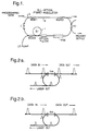
- Figure 1 shows a first example of a circuit implementing the present invention.
- a fibre laser 1 is configured in a loop and incorporates a fibre modulator 2 in the optical cavity.
- a transmission fibre 3 is also connected in common with the fibre modulator.
- the fibre laser is based on an erbium-doped fibre (operating range 1.52 - 1.66 nm) pumped by a high power laser diode LD which may be a GRINSCH InGaAsP device.
- the modulator comprises a single-mode optical fibre which, in the present example, has a length of 8.8km.
- a suitable fibre is available commercially under the trade name SMF/DS CPC3 from Corning Inc., a US corporation of Corning, New York 14831. This is a dispersion-shifted fibre designed to operate in the 1550nm region. It has a mode field diameter of 8.1 microns, a cladding diameter of 125 microns and a coating outside diameter of 250 microns.
- the effective group index of refraction is 1.476 at 1550nm.
- each of the couplers WDM1, WDM2 is a bi-directional device incorporating an interference filter formed as an evaporation-deposited stacked dielectric. One wavelength passes straight through the filter while another wavelength is reflected.
- An appropriate device having these properties is available commercially from the company JDS FITEL as WDM coupler model no.WD1515Y-A1.
- a similarly constructed wavelength-selective coupler WDM3 is used to couple a laser diode pump to the fibre laser.
- the circuit further comprises an optical filter F which may be an interference filter, used to control the frequency and width of the pulse in the laser cavity.
- An intra-cavity fibre isolator I ensures that the cavity function unidirectionally.
- a suitable isolator is model no. OIC-1100-1550 from BT & D Technologies.
- the output from the cavity is coupled by a fused fibre coupler, such as model no. SMC0202-155-OC from BT & D.
- a pulse sequence carried on the transmission fibre is input to the fibre modulator where it cross-phase modulates light propagating in the laser cavity, thereby mode-locking the laser.
- mode-locking is carried out using one of the higher harmonics of the cavity, rather than the fundamental mode.
- the laser cavity therefore contains a number of independent pulse trains.
- three data bits arrive at the modulator for every round-trip of the laser and each one of the three bits drives one of the three laser pulses in the ring.
- a repeated synchronized word is supplied to the modulator on the transmission fibre ( Figure 2b).
- the arrangement is as in Figure 2a, the only difference being that now the laser is presented with a repetitive three bit sequence ("110" in this example).
- Each bit in the three bit sequence modulates a particular pulse in the ring laser. If the data bit is a "1” then a laser pulse is generated. If the data bit is a "0” then the laser is not modulated and no laser pulse arises in that time-slot. The output of the laser is therefore modulated with the same data sequence as the input data stream.
- a laser driven at the mth harmonic of the mode-spacing can be mode-locked to a word that is m bits long, or to a word that is an integer divisor of m bits long.
- the erbium fibre ring laser is mode-locked at around 1.007GHz by a stream of ⁇ 20ps pulses drived from a gain-switched DFB laser.
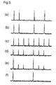
- the continuous stream applied to the fibre modulator on the transmission fibre was encoded using a LiNbO 3 amplitude modulator and a data generator. Since L, the characteristic length of the cavity, is approximately equal to 9km, giving c/nL of 23kHz, the driving frequency corresponds approximately t o the 44000th harmonic of the mode-spacing, i.e. n ⁇ 44000 so that there are 44000 pulses in the ring cavity at any one time.
- the driving data stream is set to a repetitive eight bit sequence "11010010".
- the repetition rate is tuned to a mode of the ring cavity in order to force laser mode-locking.
- a pulse can be added or subtracted from the ring cavity.
- the laser generates at its output the same "11010010" repetitive sequence.
- the laser output is in the form of a low jitter stream of near transform-limited pulses with a duration of around 10ps.
- Figure 3c shows the output of the laser when the data repetition rate is stepped one mode-spacing up or down such that there are 8n+1 or 8n-1 laser pulses respectively in the ring cavity.
- the laser output takes the form of a word where some of the bits are either "1" or "0" depending on how many 1's that bit was modulated by on average, depending also on the exact laser parameters and the data word.
- the pulse generator may also be used to carry out logic operations on the driving word.
- Figures 3(d) to 3 (f) show outputs obtained when the bit-rate is 8n+4 times the cavity frequency. Counting from left to right in the figures, the first and fifth bits see a ..111111.. pattern of driving pulses; the second, third, sixth and seventh bits see a ..101010.. pattern and the fourth and eighth bits see a ..000000.. pattern. By altering the conditions within the laser cavity, we can alter the generated pattern. In (e) and to a greater extent in (f) pulses that see a ..111111.. pattern are favoured over those that see the a ..101010.. pattern. Thus if we regard the driving word as a pair of four bit words, in (d) we see the result of an OR operation between corresponding bits in the two words and (f) we see the result of an AND operation.
- the component indicated with dashed lines in Figure 1 is an optical pulse shaping element which may optionally be included in the laser cavity.
- the inclusion of such an element changes the cavity from being entirely actively mode-locked to being partially or entirely passively mode-locked, that is a train of pulses once set up in the cavity becomes self-sustaining.
- the inclusion of such a pulse shaping element makes the circuit effective as an optical memory. That is, the programming data stream input to the modulator may be removed whilst still maintaining at the output of the laser cavity a pulse stream reproducing the pattern of the programming data.
- Such an optical memory has applications in a number of fields including optical processing or logic circuits.
- the pulse shaping element may be provided by a further fibre modulator chosen to be soliton supporting at the optical powers at which the circuit operates, or alternatively, may be formed, for example from a non-linear semiconductor wave guide. In either case, the function of the element is to sharpen the pulses in the cavity, countering the tendency of the pulses to broaden in the absence of a modulating signal in the fibre modulator.
- Figure 4 shows a remotely optically programmable OTDM (optical time-division multiplexing) network node based on an optical sequence generator in accordance with the invention.
- the steady-state operation of the device is as follows.
- the data enters a non-linear loop mirror (NOLM) at A.
- Control pulses from a pulse generating circuit PG as described above enter the loop through port E. If a control pulse is present at the loop mirror at the same time as a given data bit, then that bit is transmitted through the loop and emerges at B. Otherwise, that data bit is reflected and emerges at C. That is, the loop is in the reflecting mode in the linear regime.
- the control pulse pattern e.g. 11001000, is repeatedly output from the pulse generator PG in response to the repeated driving signal and thus only bits in the first, second and fifth channels are ever transmitted through the loop.
- This demultiplexed data passes through the fibre laser and emerges at F. Delays within the circuit are controlled so that the control word output from the pulse generator PG is bit-synchronized with the input data at the loop mirror. Then the first bit of the control pattern is coincident with the first channel of the data stream and so on.
- the node Prior to the steady-state condition described above being established, the node goes through a start-up procedure. Initially the loop mirror is biased to be partially in reflecting mode and partially in transmitting mode in the linear regime. This is done using a polarisation controller within the loop to alter the polarisation state of the light. Initially, only the channels to be demultiplexed are turned on at the input to the node. Each data pulse is partially transmitted through the loop.
- the pattern generator receives, in the present example, a repeated dd00d000 pattern where d is a data pulse which may be 1 or 0, and over several repetitions has a non-zero time-average. A pattern of the form 11001000 is generated at the output of the pulse generator and is fed back to the control pulse input of the loop.
- the non-linear phase shift imparted by the control pulses on the data in the loop increases the proportion of each pulse transmitted through the loop.
- the loop bias is then changed so that it is completely in reflecting mode in the linear regime.
- the data pulses are still transmitted however as they are coincident with the control pulses, hence the pattern generator still continues to produce the 11001000 control pulse pattern.
- the other channels are switched on then since the loop is in reflecting mode in the linear regime, and no control pulses are coincident with the data in these other channels, those channels are reflected from the loop.
- a number of such programmable network nodes may be chained together. In use, the nodes can all be programmed remotely in a cascade: that is the first (upstream) node is programmed in the manner described above, and the channels not selected at that node are then used to program the next node downstream, and so-on.
- the loop-mirror may be left permanently in a state in which it is, say, 1% transmitting in the linear regime.
- the disadvantage of this arrangement is that the extinction ratio is compromised: the demultiplexed data streams contain a small amount of light in the empty channels.
- the present invention is by no means limited in this respect and other types of optical components and circuits may be used.
- the embodiment of Figure 5 shows a pattern generator based on a hybrid semiconductor/fibre circuit.
- the first element in the circuit is a semiconductor gain medium and a saturable absorber integrated with the gain medium and arranged to be pumped by the incoming repetitive optical signal.
- the output of the semiconductor is coupled to an external fibre cavity incorporating a fibre grating end reflector.
- Figure 6 shows a further alternative embodiment using purely semiconductor components.
- the laser cavity is defined between the end walls of the semiconductor component.
- the semiconductor incorporates a saturable absorber aligned with a gain medium in a channel formed in a semiconductor substrate.
- a Bragg filter may be incorporated in the structure to tune the device to a required wavelength.
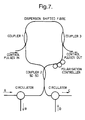
- FIG 7 shows a modified form of the loop mirror L for use in the circuit of Figure 4a.
- optical circulators C1, C2 are provided on the input and output branches of coupler 2.
- Appropriate circulators are manufactured by Optics for Research as model number OC-IR2-3 and available commercially in this country from Lambda Photometrics Limited of Harpenden, Hertfordshire.
- Such circulators in general use a crystal of the type known as a Faraday rotator. This has the property that the plane of polarisation of incident light is rotated in the same direction irrespective of the direction of travel through the crystal.
- the crystal is arranged with polarisers on its input and output such that the circulator functions as a three port device. Light entering the device at port 1 emerges from port 2, light entering at 2 emerges from 3, and light entering at port 3 emerges from 1.
- the optical control pulses applied to the loop determine the port from which a given data bit emerges.
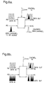
- the loop is used to drop or demultiplex one channel from an OTDM pipe and add another channel in its place.
- the data stream to be added is introduced at port PD in such a way that the pulses within that channel arrive at the same time as pulses within the channel to be dropped.
- a data pulse at port PD will emerge from port PB and hence is merged with the non-dropped part of the OTDM data stream.
- Such a function has been carried out, for example, in a system in which a 10Gbit/s channel was dropped from a 40Gbit/s data stream and another channel added in its place.
- This function can be extended to a full cross-connect function (Figure 8b), in which fully populated OTDM data streams arrive at both ports PA and PD.
- Figure 8b full cross-connect function
- An array of such devices can be used in an OTDM node, allowing data channels from several incoming pipes to be switched onto outgoing pipes.
- a fibre modulator to provide the non-linearity for the loop
- other devices may be used.
- a semiconductor amplifier may be used as the non-linear material.
- high numerical aperture (NA) optical fibres may be used.
- the network of nodes described above with respect to Figure 4b can be extended to include an ADD function as described above.
- Tributary data streams may be included in the added channels.
- the nodes are started-up in a sequence which proceeds from the first upstream node to the following downstream nodes.
- Figure 9 shows a network having a bus-type topology.
- circles denote remotely programmable nodes as described above, and squares denote data sources or terminations.
- sequence described below once a data channel has been switched on, it is left switched on.
- the appropriate start up sequence for such a bus network is then as follows:
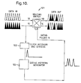
- Figure 10 shows a further example of an OTDM switching node embodying the present invention.
- the pattern generator is used in a clock recovery and division stage, and its output, rather than being applied directly to control the switch, is processed by a gating pattern generator.
- the demultiplexer of this example comprises an optical routing switch 101, providing a cross-connection between two optical inputs 1A, 1D, and two optical outputs 1B, 1C.
- the switch has a further input 1G for gating pulses which determine the setting of the switch. In the absence of a pulse at the input 1G then an optical pulse input at 1A is fed straight-through to 1B. In the presence of a pulse at input 1G a pulse input at 1A, is cross-connected to output 1C.
- the appropriate control sequence for the input G is generated by splitting one of the input optical data streams using, for example, a 50:50 fibre coupler.
- the signal is then applied to a clock recovery and division circuit 102 which generates a clock signal at, e.g., 1/n of the bit-rate of the n-channel OTDM frames.
- the resulting optical clock pulse train is passed through a gating pulse pattern generator 103 to provide the pulse sequence which is applied to the control input G.
- the clock recovery division circuit in this example is provided by a fibre-loop mirror demultiplexer as described above with reference to Figure 4a.
- This device is started up in the usual way with only one of the n channels being transmitted during the start-up sequence. As a result the output from the device is locked to the clock of the input data stream but has a repetition rate of 1/n of the original line rate.
- the gating pattern generator is shown in more detail in Figure 11. It contains a splitter/delay line/combiner arrangement 105.
- the different paths provide different respective delays for the split input optical pulse. The delays are such that each input pulse results in n output pulses, the pulse spacing being equal to the OTDM bit spacing.
- Each arm of the network contains a shutter 106 that passes or blocks light.
- the pattern of clock pulses required to gate the routing switch can be generated by controlling the status of each shutter.
- the shutters do not have to have an ultra-fast switching time so they can be electrically controlled and linked, for example, to a remote control centre responsible for configuring the network paths.
- a simple implementation of the device may use commercially available fibre couplers and solenoid-controlled moving-fibre switches. An appropriate switch is model no.
- the gating network may be an integrated device using planar silica waveguide technology.
- the shutters in such an integrated network may be semiconductor laser amplifiers SLAs.
- SLAs when turned ON can be used to provide gain, as well as carrying out the shutter function.
- Appropriate planar silica technology is disclosed in the paper by Cassidy et al, BT Technology Journal, Volume 11, Page 1377 (1993).
- the optical pathways and splitters can be formed from passive semiconductor waveguides with active overlays to define SLAs to act as shutters.
- Figure 12a shows an alternative embodiment in which instead of a single routing switch, a 2x2 array of cross-connect routing switches is used.
- This example allows four input OTDM pipes to be connected to four output pipes.
- the example shown is a blocking array. That is to say not all combinations of cross-connections are possible.
- a channel from A cannot be routed to E at the same time that B is routed to F.
- a non-blocking array could be constructed although this would require additional cross-connect routing switches.
- the corresponding non-blocking array shown in Figure 12b known as a Benes array, requires six cross-connect routing switches. In either case, only one shared clock recovery device is required.
- each cross-connect switch is to have a gating pattern independent of the others, then one gating-pulse pattern-generator is required per switch.
- the diagram shows where each input channel ends up e.g. "A3" means channel 3 from pipe A.
- Each switch is driven by a repeated six-bit pattern of control pulses.
- the control pulse patterns are:
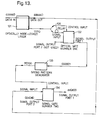
- Figure 13 shows a further example of an OTDM switching node which, as in the example described immediately above, uses a gating pattern generator.
- the data being processed has in each frame a header bit which is always set to zero. Then when such frames are applied to a first optically mode-locked laser 131 as described above with reference to Figure 1, the resulting pattern generated by the laser provides a frame synchronisation signal.
- the use of the present applicant's optical pattern generator to produce a frame synchronisation signal in this manner is proposed in the paper by M. Obro, P. Thorsen and S.B. Andreasen published at PP 1243-1244 Electronics Letters 21st July 1994, volume 30, number 15.
- the pattern is inverted. This is done by using the pattern to control a delayed version of itself input to a first optical gate 132 via a delay (e.g. a fibre loop of appropriate length) 135.
- the delay is set to be any integer number of bit periods such that the zeros within the pattern and the delayed version of the pattern are not aligned in time at the gate 132.
- a bit arriving at the signal input of the gate 132 is routed to output port 1 only from the one bit position in which there is a zero at the control input. For all other bit positions, where there is a 1 at the control input, the signal is output to port 2.
- the output from port 1 is then an inverted form of the frame synchronisation signal and this signal is fed to a gating pattern generator 133 which functions in the manner described with respect to the embodiment of Figure 10. This results in an appropriate gating pattern which is applied to a second optical gate 134, again in the fashion described above.
- the optical gates 132 and 134 may both be formed from non-linear loop mirrors in which the two pulse trains involved are distinguished by having orthogonal polarisations.
- the two pulse streams involved are at the same wavelength, by contrast with the previous examples in which signals were distinguished by different wavelengths, and the different polarisation states are therefore needed to separate the different pulse streams.
- the pattern of gating pulses produced by the pattern generator 133 is 110100.
Landscapes
- Physics & Mathematics (AREA)
- Electromagnetism (AREA)
- Optics & Photonics (AREA)
- Engineering & Computer Science (AREA)
- Computer Networks & Wireless Communication (AREA)
- Nonlinear Science (AREA)
- Signal Processing (AREA)
- Plasma & Fusion (AREA)
- General Physics & Mathematics (AREA)
- Condensed Matter Physics & Semiconductors (AREA)
- Optical Communication System (AREA)
- Lasers (AREA)
- Microscoopes, Condenser (AREA)
- Semiconductor Lasers (AREA)
- Small-Scale Networks (AREA)
Claims (20)
- Procédé de génération d'une séquence d'impulsions optiques comprenant l'application d'un signal optique répétitif à un modulateur optique (2) connecté dans la cavité de laser d'un laser asservi en mode (1 ; 131) et la sortie d'une séquence d'impulsions depuis la cavité du laser, caractérisé en ce que la période de répétition du signal optique répétitif est égale au temps d'aller et retour de la cavité, ou bien à un multiple entier de celui-ci, le laser étant ainsi attaqué de façon à fournir en sortie des impulsions à des positions de bits qui correspondent aux impulsions non nulles du signal optique répétitif d'entrée.
- Procédé selon la revendication 1, dans lequel le laser est agencé de façon à continuer à sortir la séquence d'impulsions après que le signal optique répétitif d'entrée a été supprimé ou modifié.
- Procédé selon la revendication 2, comprenant l'étape consistant à faire passer des impulsions dans la cavité du laser au travers d'un élément de mise en forme d'impulsions (PSE) agencé pour raccourcir les impulsions.
- Procédé de commande d'un commutateur optique,caractérisé par l'application d'un signal optique répétitif à un modulateur (2) connecté dans la cavité optique d'un laser (1 ; 131) en asservissant ainsi le laser en mode, la période de répétition du signal optique répétitif étant égale au temps d'aller et retour de la cavité ou bien à un multiple entier de celui-ci,fournir en sortie le train d'impulsions généré dans la cavité en réponse au signal optique répétitif appliqué, etappliquer le train d'impulsions ou bien un signal obtenu à partir de celui-ci, à l'entrée de commande (1G) d'un commutateur optique (101 ; 132) conçu pour acheminer des données entrantes vers des sorties différentes en fonction de l'état du signal au niveau de l'entrée de commande.
- Procédé selon la revendication 4, dans lequel des signaux provenant de l'une des sorties du commutateur optique sont appliqués au modulateur dans la cavité optique afin d'obtenir ledit signal optique répétitif.
- Procédé selon la revendication 5, comprenant en outre l'établissement du commutateur optique dans un état dans lequel au moins une partie de chaque impulsion d'entrée est fournie en sortie au niveau de ladite une sortie, indépendamment de l'état de l'entrée de commande, et dans lequel le flux de données au niveau de l'entrée est établi de façon à être non nul uniquement dans les positions de bits qui correspondent aux canaux OTDM (multiplexage optique par partage de temps) qui doivent être sélectionnés par ledit multiplexeur comprenant ledit commutateur.
- Procédé selon l'une quelconque des revendications 4 à 6, dans lequel un premier flux de données OTDM et un ou plusieurs canaux de données supplémentaires sont appliqués en entrée au commutateur, et le ou chaque canal de données supplémentaire est remplacé dans le flux de données fourni en sortie à partir du commutateur.
- Procédé selon la revendication 7, dans lequel l'entrée vers le commutateur comprend au moins deux flux de données OTDM et le commutateur commute les canaux par croisement entre les différents flux de données en réponse au signal au niveau de son entrée de commande.
- Procédé selon la revendication 4, dans lequel ledit commutateur optique fournit en sortie, en réponse au signal de commande au niveau de l'entrée de commande, un signal d'horloge récupéré à un diviseur entier de la fréquence d'horloge du flux de données en entrée.
- Procédé selon la revendication 9, comprenant en outre l'application du signal d'horloge récupéré à un générateur de séquences d'aiguillage (103 ; 105 ; 133), et l'application du signal fourni en sortie par le générateur de séquences d'aiguillage à l'entrée de commande d'un autre commutateur optique (134), l'autre commutateur optique commutant ledit flux de données entre une pluralité de sorties en réponse au signal d'aiguillage au niveau de l'entrée de commande.
- Procédé selon la revendication 9 ou la revendication 10, dans lequel le signal optique répétitif comprend des trames de données OTDM, la totalité des trames de données comportant un en-tête incluant une valeur nulle à une position de bit prédéterminée, le laser à mode asservi générant ainsi un signal de synchronisation de trame.
- Procédé selon la revendication 11, comprenant en outre l'inversion du signal de synchronisation de trame, et l'application du signal inversé à un générateur de séquences d'aiguillage en produisant ainsi le signal de commande pour le commutateur optique.
- Système de commutation optique comprenantun commutateur optique (101 ; 132) comportant au moins une entrée de signal et une pluralité de sorties de signaux ainsi qu'une entrée de commande, etun générateur de séquences d'impulsions optiques (PG) comprenant un laser à mode asservi (1 ; 131) comportant un modulateur (2) connecté dans la cavité du laser et comprenant une entrée destinée à un signal optique répétitif qui, en utilisation, est appliqué au modulateur, la cavité présentant un temps d'aller et retour tel que la période de répétition du signal optique répétitif soit égale audit temps d'aller et retour ou à un multiple entier de celui-ci,la sortie du générateur de séquences d'impulsions optiques étant reliée directement ou indirectement à l'entrée de commande (1G) du commutateur optique (101) et le commutateur acheminant ainsi des données entrantes vers des sorties différentes en fonction de l'état du signal au niveau de l'entrée de commande.
- Système selon la revendication 13, dans lequel une sortie du commutateur optique est reliée à l'entrée du générateur de séquences d'impulsions afin de fournir ledit signal optique répétitif.
- Système selon la revendication 14, comprenant un moyen destiné à établir le commutateur optique, pendant une phase de lancement, dans un état de transmission partielle dans lequel tous les signaux entrants sont, au moins en partie, transmis vers ladite sortie reliée au générateur de séquences d'impulsions, indépendamment de l'état de l'entrée de commande.
- Système selon l'une quelconque des revendications 13 à 15, dans lequel le commutateur comprend une première entrée destinée à un flux de données OTDM, et une seconde entrée destinée à un ou plusieurs canaux OTDM supplémentaires, et est conçu pour remplacer les un ou plusieurs canaux supplémentaires dans la sortie du flux de données à partir du commutateur.
- Système selon la revendication 16, dans lequel le commutateur comprend des entrées destinées à deux flux de données OTDM, et est conçu pour commuter les canaux de façon croisée entre les deux flux de données en réponse au signal à l'entrée de commande.
- Système selon l'une quelconque des revendications 13 à 17, dans lequel le commutateur (132) est conçu, en réponse au signal de commande provenant du générateur de séquences d'impulsions, de façon à fournir en sortie un signal d'horloge récupéré à un diviseur entier de la fréquence d'horloge d'un flux de données en entrée, le système comprenant en outre un générateur de séquences d'aiguillage (132) relié à une sortie de commutateur optique, et conçu de façon à générer, à partir du signal d'horloge récupéré , un signal de commande destiné à un autre commutateur optique (134), conçu pour recevoir ledit flux de données.
- Système selon la revendication 18, dans lequel la sortie de signal provenant du générateur de séquences d'impulsions est un signal de synchronisation de trame produit en réponse à des trames de données OTDM présentant toutes une valeur nulle à une position de bit d'en-tête prédéterminée, et dans lequel le commutateur optique reliés à la sortie du générateur de séquences d'impulsions est conçu de façon à inverser le signal de synchronisation de trame.
- Système selon l'une quelconque des revendications 13 à 19, dans lequel le commutateur optique et/ou l'autre commutateur optique comprend un miroir à boucle non linéaire (NOLM).
Priority Applications (1)
| Application Number | Priority Date | Filing Date | Title |
|---|---|---|---|
| EP94928988A EP0723716B1 (fr) | 1993-10-11 | 1994-10-11 | Generateur de sequence d'impulsions optiques |
Applications Claiming Priority (8)
| Application Number | Priority Date | Filing Date | Title |
|---|---|---|---|
| EP93308067 | 1993-10-11 | ||
| EP93308067 | 1993-10-11 | ||
| GB9406882 | 1994-04-07 | ||
| GB9406882A GB9406882D0 (en) | 1994-04-07 | 1994-04-07 | Optical pulse sequence generator |
| EP94303193 | 1994-05-03 | ||
| EP94303193 | 1994-05-03 | ||
| PCT/GB1994/002239 WO1995010870A1 (fr) | 1993-10-11 | 1994-10-11 | Generateur de sequence d'impulsions optiques |
| EP94928988A EP0723716B1 (fr) | 1993-10-11 | 1994-10-11 | Generateur de sequence d'impulsions optiques |
Publications (2)
| Publication Number | Publication Date |
|---|---|
| EP0723716A1 EP0723716A1 (fr) | 1996-07-31 |
| EP0723716B1 true EP0723716B1 (fr) | 1998-11-25 |
Family
ID=27235507
Family Applications (1)
| Application Number | Title | Priority Date | Filing Date |
|---|---|---|---|
| EP94928988A Expired - Lifetime EP0723716B1 (fr) | 1993-10-11 | 1994-10-11 | Generateur de sequence d'impulsions optiques |
Country Status (10)
| Country | Link |
|---|---|
| US (1) | US5796765A (fr) |
| EP (1) | EP0723716B1 (fr) |
| JP (1) | JPH09505688A (fr) |
| CN (1) | CN1096137C (fr) |
| AU (1) | AU676387B2 (fr) |
| CA (1) | CA2171337C (fr) |
| DE (1) | DE69414876T2 (fr) |
| DK (1) | DK0723716T3 (fr) |
| ES (1) | ES2126153T3 (fr) |
| WO (1) | WO1995010870A1 (fr) |
Families Citing this family (14)
| Publication number | Priority date | Publication date | Assignee | Title |
|---|---|---|---|---|
| DE19529376A1 (de) * | 1995-08-10 | 1997-02-13 | Sel Alcatel Ag | Optisches TDMA-Ringnetz mit einer zentralen Sende- und Empfangseinrichtung |
| WO1997042543A1 (fr) * | 1996-05-08 | 1997-11-13 | British Telecommunications Public Limited Company | Division d'horloge d'un signal optique |
| JP3145941B2 (ja) * | 1997-01-13 | 2001-03-12 | 日本電気株式会社 | 光機能増幅素子及びその動作方法 |
| GB9719895D0 (en) * | 1997-09-18 | 1997-11-19 | British Telecomm | A method of obtaining an optical signal stream |
| CA2299236A1 (fr) * | 1998-02-20 | 1999-08-26 | Brian L. Lawrence | Amplificateur optique et procede pour amplifier un signal optique se propageant dans une fibre optique en utilisant un guide d'ondes de recouvrement et une emission stimulee |
| JP3961153B2 (ja) * | 1999-05-14 | 2007-08-22 | 富士通株式会社 | 光クロックの再生及び適用のための方法、装置及びシステム |
| WO2002063729A1 (fr) * | 2001-02-08 | 2002-08-15 | Frame Photonics | Generation de multiples longueurs d'ondes auto-triees |
| US7840495B2 (en) * | 2001-08-03 | 2010-11-23 | Jay Levenson | System and method for the payment and accounting of petty disbursements |
| WO2004107510A2 (fr) * | 2003-06-03 | 2004-12-09 | Kilolambda Technologies Ltd. | Generateur d'impulsions laser |
| EP2662674A3 (fr) * | 2007-01-19 | 2014-06-25 | The General Hospital Corporation | Réflexion de disque rotatif pour balayage rapide de longueur d'onde de lumière à large bande dispersée |
| RU2432670C1 (ru) * | 2010-07-26 | 2011-10-27 | Михаил Александрович Аллес | Оптический генератор импульсных последовательностей |
| US20140084794A1 (en) * | 2012-09-22 | 2014-03-27 | Richard Jeff Garcia | Method for programming a LED light using a light sensor |
| JP2015103831A (ja) | 2013-11-21 | 2015-06-04 | 富士通株式会社 | 光分岐装置および光挿入装置 |
| US10389558B2 (en) * | 2016-10-03 | 2019-08-20 | Mediatek Inc. | Method and apparatus for synchronization |
Family Cites Families (5)
| Publication number | Priority date | Publication date | Assignee | Title |
|---|---|---|---|---|
| GB2269699B (en) * | 1991-03-01 | 1995-01-25 | Telstra Corp Ltd | Modelocked lasers |
| FR2700895B1 (fr) * | 1993-01-28 | 1995-03-03 | Jean Debeau | Procédé et dispositif de génération d'impulsions optiques. |
| JPH06318754A (ja) * | 1993-05-10 | 1994-11-15 | Matsushita Electric Ind Co Ltd | 光ファイバ増幅器および光信号伝送システム |
| IT1272640B (it) * | 1993-09-16 | 1997-06-26 | Pirelli Cavi Spa | Generatore laser a fibra ottica a concatenamento modale passivo a commutazione non lineare di polarizzazione |
| US5513194A (en) * | 1994-06-30 | 1996-04-30 | Massachusetts Institute Of Technology | Stretched-pulse fiber laser |
-
1994
- 1994-10-11 DE DE69414876T patent/DE69414876T2/de not_active Expired - Fee Related
- 1994-10-11 CA CA002171337A patent/CA2171337C/fr not_active Expired - Fee Related
- 1994-10-11 DK DK94928988T patent/DK0723716T3/da active
- 1994-10-11 CN CN94193716A patent/CN1096137C/zh not_active Expired - Fee Related
- 1994-10-11 WO PCT/GB1994/002239 patent/WO1995010870A1/fr not_active Ceased
- 1994-10-11 EP EP94928988A patent/EP0723716B1/fr not_active Expired - Lifetime
- 1994-10-11 AU AU78209/94A patent/AU676387B2/en not_active Ceased
- 1994-10-11 ES ES94928988T patent/ES2126153T3/es not_active Expired - Lifetime
- 1994-10-11 JP JP7511481A patent/JPH09505688A/ja not_active Ceased
-
1996
- 1996-06-24 US US08/617,868 patent/US5796765A/en not_active Expired - Lifetime
Also Published As
| Publication number | Publication date |
|---|---|
| DK0723716T3 (da) | 1999-08-09 |
| JPH09505688A (ja) | 1997-06-03 |
| WO1995010870A1 (fr) | 1995-04-20 |
| ES2126153T3 (es) | 1999-03-16 |
| US5796765A (en) | 1998-08-18 |
| CA2171337A1 (fr) | 1995-04-20 |
| CN1133652A (zh) | 1996-10-16 |
| CA2171337C (fr) | 2000-03-28 |
| EP0723716A1 (fr) | 1996-07-31 |
| DE69414876T2 (de) | 1999-04-22 |
| CN1096137C (zh) | 2002-12-11 |
| DE69414876D1 (de) | 1999-01-07 |
| AU676387B2 (en) | 1997-03-06 |
| AU7820994A (en) | 1995-05-04 |
Similar Documents
| Publication | Publication Date | Title |
|---|---|---|
| EP0761050B1 (fr) | Traitement optique de paquets | |
| Dorren et al. | Optical packet switching and buffering by using all-optical signal processing methods | |
| US5307428A (en) | Optical domain digital pulse switching | |
| Calabretta et al. | Optical signal processing based on self-induced polarization rotation in a semiconductor optical amplifier | |
| AU676387B2 (en) | Optical pulse sequence generator | |
| EP0804751A1 (fr) | Commutateur optique | |
| Vlachos et al. | Ultrafast time-domain technology and its application in all-optical signal processing | |
| EP1255157A1 (fr) | Modulation de l'intensité d'un signal optique | |
| US6344913B1 (en) | Optical clock division | |
| JP4844405B2 (ja) | 光クロック信号再生装置 | |
| JP3455723B2 (ja) | 光時分割多重光スイッチ | |
| Lucek et al. | Remotely programmable routing device with optical clock division | |
| Liu et al. | All-optical signal processing for optical packet switching networks | |
| AU690797C (en) | Optical switch | |
| EP0987844B1 (fr) | Dispositif optique de traitement d'une impulsion optique | |
| Wang | All optical signal processing for hybrid OTDM/WDM switching networks | |
| Agarwal | All-optical loadable and erasable fiber storage buffer based on parametric nonlinearity in fiber | |
| Toliver | Scaling issues in photonic packet switching networks based on optical TDM | |
| Vlachos et al. | A system perspective of all-optical digital logic gates |
Legal Events
| Date | Code | Title | Description |
|---|---|---|---|
| PUAI | Public reference made under article 153(3) epc to a published international application that has entered the european phase |
Free format text: ORIGINAL CODE: 0009012 |
|
| 17P | Request for examination filed |
Effective date: 19960215 |
|
| AK | Designated contracting states |
Kind code of ref document: A1 Designated state(s): BE CH DE DK ES FR GB IT LI NL PT SE |
|
| GRAG | Despatch of communication of intention to grant |
Free format text: ORIGINAL CODE: EPIDOS AGRA |
|
| 17Q | First examination report despatched |
Effective date: 19971215 |
|
| GRAG | Despatch of communication of intention to grant |
Free format text: ORIGINAL CODE: EPIDOS AGRA |
|
| GRAH | Despatch of communication of intention to grant a patent |
Free format text: ORIGINAL CODE: EPIDOS IGRA |
|
| GRAH | Despatch of communication of intention to grant a patent |
Free format text: ORIGINAL CODE: EPIDOS IGRA |
|
| GRAA | (expected) grant |
Free format text: ORIGINAL CODE: 0009210 |
|
| AK | Designated contracting states |
Kind code of ref document: B1 Designated state(s): BE CH DE DK ES FR GB IT LI NL PT SE |
|
| REG | Reference to a national code |
Ref country code: CH Ref legal event code: NV Representative=s name: JACOBACCI & PERANI S.A. Ref country code: CH Ref legal event code: EP |
|
| REF | Corresponds to: |
Ref document number: 69414876 Country of ref document: DE Date of ref document: 19990107 |
|
| ET | Fr: translation filed | ||
| REG | Reference to a national code |
Ref country code: ES Ref legal event code: FG2A Ref document number: 2126153 Country of ref document: ES Kind code of ref document: T3 |
|
| REG | Reference to a national code |
Ref country code: PT Ref legal event code: SC4A Free format text: AVAILABILITY OF NATIONAL TRANSLATION Effective date: 19981130 |
|
| REG | Reference to a national code |
Ref country code: DK Ref legal event code: T3 |
|
| PGFP | Annual fee paid to national office [announced via postgrant information from national office to epo] |
Ref country code: DK Payment date: 19990914 Year of fee payment: 6 |
|
| PGFP | Annual fee paid to national office [announced via postgrant information from national office to epo] |
Ref country code: NL Payment date: 19990921 Year of fee payment: 6 |
|
| PGFP | Annual fee paid to national office [announced via postgrant information from national office to epo] |
Ref country code: PT Payment date: 19990929 Year of fee payment: 6 |
|
| PLBE | No opposition filed within time limit |
Free format text: ORIGINAL CODE: 0009261 |
|
| STAA | Information on the status of an ep patent application or granted ep patent |
Free format text: STATUS: NO OPPOSITION FILED WITHIN TIME LIMIT |
|
| PGFP | Annual fee paid to national office [announced via postgrant information from national office to epo] |
Ref country code: BE Payment date: 19991004 Year of fee payment: 6 |
|
| PGFP | Annual fee paid to national office [announced via postgrant information from national office to epo] |
Ref country code: ES Payment date: 19991006 Year of fee payment: 6 |
|
| 26N | No opposition filed | ||
| REG | Reference to a national code |
Ref country code: GB Ref legal event code: 732E |
|
| PG25 | Lapsed in a contracting state [announced via postgrant information from national office to epo] |
Ref country code: DK Free format text: LAPSE BECAUSE OF NON-PAYMENT OF DUE FEES Effective date: 20001011 |
|
| PG25 | Lapsed in a contracting state [announced via postgrant information from national office to epo] |
Ref country code: ES Free format text: LAPSE BECAUSE OF NON-PAYMENT OF DUE FEES Effective date: 20001012 |
|
| PG25 | Lapsed in a contracting state [announced via postgrant information from national office to epo] |
Ref country code: BE Free format text: LAPSE BECAUSE OF NON-PAYMENT OF DUE FEES Effective date: 20001031 |
|
| BERE | Be: lapsed |
Owner name: BRITISH TELECOMMUNICATIONS P.L.C. Effective date: 20001031 |
|
| PG25 | Lapsed in a contracting state [announced via postgrant information from national office to epo] |
Ref country code: PT Free format text: LAPSE BECAUSE OF NON-PAYMENT OF DUE FEES Effective date: 20010430 |
|
| PG25 | Lapsed in a contracting state [announced via postgrant information from national office to epo] |
Ref country code: NL Free format text: LAPSE BECAUSE OF NON-PAYMENT OF DUE FEES Effective date: 20010501 |
|
| REG | Reference to a national code |
Ref country code: DK Ref legal event code: EBP |
|
| NLV4 | Nl: lapsed or anulled due to non-payment of the annual fee |
Effective date: 20010501 |
|
| PGFP | Annual fee paid to national office [announced via postgrant information from national office to epo] |
Ref country code: CH Payment date: 20010919 Year of fee payment: 8 |
|
| PGFP | Annual fee paid to national office [announced via postgrant information from national office to epo] |
Ref country code: SE Payment date: 20010920 Year of fee payment: 8 |
|
| REG | Reference to a national code |
Ref country code: GB Ref legal event code: IF02 |
|
| PG25 | Lapsed in a contracting state [announced via postgrant information from national office to epo] |
Ref country code: SE Free format text: LAPSE BECAUSE OF NON-PAYMENT OF DUE FEES Effective date: 20021012 |
|
| PG25 | Lapsed in a contracting state [announced via postgrant information from national office to epo] |
Ref country code: LI Free format text: LAPSE BECAUSE OF NON-PAYMENT OF DUE FEES Effective date: 20021031 Ref country code: CH Free format text: LAPSE BECAUSE OF NON-PAYMENT OF DUE FEES Effective date: 20021031 |
|
| EUG | Se: european patent has lapsed | ||
| REG | Reference to a national code |
Ref country code: CH Ref legal event code: PL |
|
| REG | Reference to a national code |
Ref country code: ES Ref legal event code: FD2A Effective date: 20011113 |
|
| PG25 | Lapsed in a contracting state [announced via postgrant information from national office to epo] |
Ref country code: IT Free format text: LAPSE BECAUSE OF NON-PAYMENT OF DUE FEES;WARNING: LAPSES OF ITALIAN PATENTS WITH EFFECTIVE DATE BEFORE 2007 MAY HAVE OCCURRED AT ANY TIME BEFORE 2007. THE CORRECT EFFECTIVE DATE MAY BE DIFFERENT FROM THE ONE RECORDED. Effective date: 20051011 |
|
| PGFP | Annual fee paid to national office [announced via postgrant information from national office to epo] |
Ref country code: FR Payment date: 20080922 Year of fee payment: 15 |
|
| PGFP | Annual fee paid to national office [announced via postgrant information from national office to epo] |
Ref country code: GB Payment date: 20080919 Year of fee payment: 15 |
|
| PGFP | Annual fee paid to national office [announced via postgrant information from national office to epo] |
Ref country code: DE Payment date: 20080923 Year of fee payment: 15 |
|
| REG | Reference to a national code |
Ref country code: FR Ref legal event code: ST Effective date: 20100630 |
|
| PG25 | Lapsed in a contracting state [announced via postgrant information from national office to epo] |
Ref country code: FR Free format text: LAPSE BECAUSE OF NON-PAYMENT OF DUE FEES Effective date: 20091102 Ref country code: DE Free format text: LAPSE BECAUSE OF NON-PAYMENT OF DUE FEES Effective date: 20100501 |
|
| PG25 | Lapsed in a contracting state [announced via postgrant information from national office to epo] |
Ref country code: GB Free format text: LAPSE BECAUSE OF NON-PAYMENT OF DUE FEES Effective date: 20091011 |