EP0724226A2 - Dispositif de lecture/écriture de carte à puce - Google Patents
Dispositif de lecture/écriture de carte à puce Download PDFInfo
- Publication number
- EP0724226A2 EP0724226A2 EP96100706A EP96100706A EP0724226A2 EP 0724226 A2 EP0724226 A2 EP 0724226A2 EP 96100706 A EP96100706 A EP 96100706A EP 96100706 A EP96100706 A EP 96100706A EP 0724226 A2 EP0724226 A2 EP 0724226A2
- Authority
- EP
- European Patent Office
- Prior art keywords
- card
- plate
- writer
- members
- section
- Prior art date
- Legal status (The legal status is an assumption and is not a legal conclusion. Google has not performed a legal analysis and makes no representation as to the accuracy of the status listed.)
- Granted
Links
Images


Classifications
-
- G—PHYSICS
- G06—COMPUTING OR CALCULATING; COUNTING
- G06K—GRAPHICAL DATA READING; PRESENTATION OF DATA; RECORD CARRIERS; HANDLING RECORD CARRIERS
- G06K7/00—Methods or arrangements for sensing record carriers, e.g. for reading patterns
- G06K7/0013—Methods or arrangements for sensing record carriers, e.g. for reading patterns by galvanic contacts, e.g. card connectors for ISO-7816 compliant smart cards or memory cards, e.g. SD card readers
- G06K7/0021—Methods or arrangements for sensing record carriers, e.g. for reading patterns by galvanic contacts, e.g. card connectors for ISO-7816 compliant smart cards or memory cards, e.g. SD card readers for reading/sensing record carriers having surface contacts
-
- G—PHYSICS
- G06—COMPUTING OR CALCULATING; COUNTING
- G06K—GRAPHICAL DATA READING; PRESENTATION OF DATA; RECORD CARRIERS; HANDLING RECORD CARRIERS
- G06K19/00—Record carriers for use with machines and with at least a part designed to carry digital markings
- G06K19/06—Record carriers for use with machines and with at least a part designed to carry digital markings characterised by the kind of the digital marking, e.g. shape, nature, code
- G06K19/067—Record carriers with conductive marks, printed circuits or semiconductor circuit elements, e.g. credit or identity cards also with resonating or responding marks without active components
- G06K19/07—Record carriers with conductive marks, printed circuits or semiconductor circuit elements, e.g. credit or identity cards also with resonating or responding marks without active components with integrated circuit chips
- G06K19/077—Constructional details, e.g. mounting of circuits in the carrier
- G06K19/07737—Constructional details, e.g. mounting of circuits in the carrier the record carrier consisting of two or more mechanically separable parts
- G06K19/07741—Constructional details, e.g. mounting of circuits in the carrier the record carrier consisting of two or more mechanically separable parts comprising a first part operating as a regular record carrier and a second attachable part that changes the functional appearance of said record carrier, e.g. a contact-based smart card with an adapter part which, when attached to the contact card makes the contact card function as a non-contact card
Definitions
- the present invention relates to an IC card reader/writer which can read information from or write information to, a thin-film type IC card for example.
- a processing apparatus for reading information from, or writing information to, a thin-type IC card is placed as an external apparatus and used to be connected by a connector cable, etc., to an interface, such as RS-232C, of a computer apparatus.
- the conventional processing device is of a box-like structure with an IC card set therein. This structure not only can protect internal component parts but also can protect and position the card.
- a contact holder holds contact pins in the box-like structure and is adapted to be moved up and down to allow the contact pins to be moved toward and away from an IC card inserted in the box-like structure.
- the IC card reader/writer cannot be made thinner and be inserted into a slot in a standardized card type device in a hand-held computer.
- an IC card reader/writer comprising first and second members arranged in a spaced-apart relation through supporting means provided between one-end sides thereof to define an IC card storage space between opposed surfaces thereof and, upon insertion of the IC card into the IC card storage space, providing an external shape substantially equal to that of a standard card, the reader/writer being insertable into, and withdrawable out of, a standard card holding section of an associated information processing apparatus via a one-end side.
- the IC card can be used for an information processing apparatus, such as a hand-held personal computer, which has been used for standard cards.
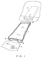
- FIG. 1 is a perspective view showing a computer 1, such as a notebook type personal computer as an information processing apparatus, an IC card reader/writer 3 and an IC card 5.
- a computer 1 such as a notebook type personal computer as an information processing apparatus, an IC card reader/writer 3 and an IC card 5.
- the computer apparatus 1 has an insertion inlet 1a at its front side to allow a card-type device to be inserted and a card holding section 2 provided for accommodating various kinds of cards, for example, a PC card (PCMCIA standard card) such as a memory card.
- the card holding section 2 is so dimensioned as to have a shape substantially satisfying the card standard.
- An associated connection area connected to the PC card is provided in the card holding section 2.
- the IC card reader/writer 3 is inserted via the insertion inlet 1a into the card holding section 2 of the computer apparatus 1 and has an LED 12 and eject button 13 on a side opposite to the insertion inlet 1a side.
- the IC card 5 has an IC (integrated circuit) terminal 6 and is inserted into the IC card reader/writer 3 and held there.
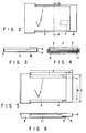
- FIG. 2 is a top view showing the IC card reader/writer 3.
- reference numeral 4 shows a main unit as a first member.
- the main unit 4 includes a contact block 7 comprised of eight pins making contact with the IC terminal 6 of the IC card 5, an ejecting mechanism, not shown, for ejecting the IC card 5, and so on.
- the main unit 4 has a connector section 10 at one end which serves as a first support section.
- FIG. 3 is a front view showing the IC card reader/writer 3.
- reference numeral 8 shows a base frame formed of metal or a molding and serving as a second member.
- the base frame 8 principally protects the undersurface of the IC card 5 and enables the terminal 6 of the IC card 5 to be placed in positive contact with the contact block 7.
- the base frame 8 and main unit 4 are spaced over 0.76 mm away from each other and, between their opposed surfaces, define a storage space 11 for holding the IC card therein.
- FIG. 4 is a cross-sectional view, taken along line IV-IV in FIG. 2.
- the IC card 5 is inserted into the storage space 11 between the base frame 8 and the main unit 4 and held therein.
- FIG. 5 is a bottom view showing the IC card reader/writer.
- the main unit 4 has a width dimension a of 54 mm equal to the width dimension of the standard PC card and the base frame 8 and main unit 4 are T-like in configuration.
- the base frame 8 has a width dimension b of below 48 mm at its narrower end section.
- the base frame 8 has a length dimension c corresponding to a length obtained by subtracting, from a dimension e (above 85.6 mm) from the forward end of the connector section 10, a dimension d (above 10 mm) from the forward end of the connector section 10 in FIG. 5.
- the section of the base frame 8 of the length dimension C is inserted in the card holding section 2 and the broader section thereof is externally projected from the card holding section 2.
- FIG. 6 is a side view showing the IC card reader/writer 3.
- the opposed one-end sides of the base frame 8 and main unit 4 are supported through the connector section 10 serving as the support section and the other-end sides of the base frame 8 and main unit 4 are supported through bent sections 9, 9 serving as second supports.
- FIG. 7 is a perspective, exploded view showing the IC card reader/writer.
- the lower surface of the connector section 10 of the main unit 4 is bonded by a bonding agent 15 to the upper surface of the one end side of the base frame 8. Both the side surfaces of the wider end section of the main unit 4 are fixedly bonded by the bonding agent 15 to the opposed inner surfaces of the upper side portions of the bent sections 9, 9 of the base frame 8.
- the non-insertion-side end that is, the bent sections 9, 9 of the base frame 8 and wider end section of the main unit 4 supported by the bent sections 9, 9 are externally positioned without being inserted into the computer apparatus 1.
- the externally positioned bent sections 9, 9 have their spaced-apart width dimension correspond to the width dimension of the IC card 5.
- the opposed surfaces 9a, 9a of the bent sections 9, 9 provide guide surfaces and, upon insertion of the IC card 5, serves as a guide means.
- the IC card reader/writer 3 of the present invention has its main section so dimensioned as to substantially correspond to the standard of the card type device and, in a practical form, the reader/writer 3 has a dimension of 5 mm at max. in a thickness direction and a wide dimension of 54 mm corresponding to that of the IC card 5 with a large scale integrated (LSI) circuit 6 mounted therein.
- LSI large scale integrated
- an external shape defined by both the insertion section of the IC card reader/writer 3 into the computer apparatus 1 and IC card 5 substantially corresponds to that of the standard card-type device.
- the IC card reader/writer 3 with the IC card 5 inserted therein is set in the card holding section 2 of the computer apparatus 1 via the insertion inlet 1a as shown in FIG. 4.
- the IC card 5 is first inserted into the storage space 11 of the reader/writer 3 and, at this time of insertion, the IC card 5 is set in a predetermined position in the storage space 11 while being guided along the opposed surfaces 9a, 9a of the bent sections 9, 9 of the base frame 8. Then, the reader/writer 3 with the IC card 5 inserted therein is inserted into the card holding section 2 of the personal computer 1 via the insertion inlet 1. By doing so, the connection section 10 of the reader/writer 3 is electrically connected to an associated connection area of the PC card in the computer apparatus 1 and set in a ready state.
- the IC card reader/writer 3 can be set in the personal computer apparatus 1 at the card holding section 2 for a standardized memory card and so on, it can be used as one unit with the computer apparatus 1 and carried about with him or her. As a result, it can be freely used from place to place and is very convenient.
- the base frame 8 and main unit 4 are partially fixed at their end sections and their width dimension can be made smaller than the width dimension (54 mm) of the IC card 5, so that the base frame/main unit structure can be readily set in the card holding section 2 for those cards such as the standardized memory cards.
- the opposed surfaces 9a, 9a of the bent sections 9, 9 of the base frame 8 which are projected from the insertion inlet 1a of the computer apparatus 1 serve as the guide sections at the insertion of the IC card 5, it is possible to insert the IC card 5 in a correct direction without being tilted.
- FIG. 8 shows an IC card reader/writer 20 according to another embodiment of the present invention.
- Elongated holes 21, 21 are provided in bent section 9, 9, respectively, of a one-end side of a base frame 8 of an IC card reader/writer 20 and engaging claws 21, 21 are provided on an other-end side of the base frame 8.
- a main unit 4 has projections 23, 23 at both opposite end portions of its wide-end side and engaging holes 24, 24 at its non-wide end side.
- the main unit 4 is mounted on the base frame 8 with its projections 23, 23 fitted in the elongated holes 21, 21 in the bent sections 9, 9 of the base frame 8 and its engaging holes 24, 24, that is, its engaging holes 24, 24 on a connector section 10 side, fitted over engaging claws 22, 22 of the base frame 8.
- FIGS. 9 to 13 show a third embodiment of the present invention.
- FIG. 9 shows a computer apparatus 1, such as a notebook type personal computer, serving as an information processing apparatus, an IC card reader/writer 31 and an IC card 5.
- a computer apparatus such as a notebook type personal computer, serving as an information processing apparatus, an IC card reader/writer 31 and an IC card 5.
- the computer apparatus 1 has an insertion inlet 1a at the front face side to allow a card-type device to be inserted therein and a card holding section 2 therein which has a dimension of a shape substantially corresponding to various kinds of card standards.
- the IC card reader/writer 31 is inserted into the computer apparatus 1 via the insertion inlet 1a to have its connector section 10 electrically connected to an associated connection section in the computer apparatus 1.
- the IC card reader/writer 31 has its greater portion so dimensioned as to have a shape substantially corresponding to a card type device standard and, in a practical form, have a thickness of 5 mm at max. and a width of 54 mm equal to the dimension of the IC card 5 with an LSI (large scale integrated) circuit 6 mounted therein.
- FIG. 10 is a top view showing the IC card reader/writer 31.
- the IC card reader/writer 31 has a main unit 35 as a first member.
- a contact block 37 comprised of eight pins is provided at the main unit 35 to allow it to make contact with the IC card 5 and an ejecting mechanism, etc., not shown, is provided at the main unit 35 to eject the IC card out of the reader/writer 31.
- FIG. 11 is a side view showing the IC card reader/writer 31.
- reference numeral 36 shows a base frame as a second member.
- the base frame 36 has the main function of protecting the undersurface of the IC card 5 and ensuring positive contact of the contact block 37 with an IC terminal.
- FIG. 12 is a front view showing an IC card reader/writer 31.
- the main unit 35 and base frame 36 are spaced over 0.76 mm apart from each other to define an IC card storage space between their opposed surfaces.
- FIG. 13 is a bottom view showing the IC card reader/writer 31.
- the main unit 35 has a width dimension a of 54 mm equal to that of the IC card 5 and a length dimension b of 85.6 mm and the base frame 36 has a width dimension c of below 48 mm.
- the IC card reader/writer 31 is different in configuration from those of the above-mentioned embodiments and is of such a type that it can be completely inserted into the computer apparatus 1.
- main unit 35 is only 54 mm in width dimension the same as that of the IC card 5, so that the main unit is fixed to the base frame 36 at one place or that the main unit is made integral with the base frame 36.
- a connector section 10 of the main unit 35 is fixed at its lower surface portion to the base frame 36 by means of a bonding agent 39.
- main unit 35 is to be formed integral with the base frame 36, they are molded in one piece form.
- the final configuration of the IC card reader/writer 31 takes on a U-shape as seen in a side view in FIG. 11.
Landscapes
- Engineering & Computer Science (AREA)
- Physics & Mathematics (AREA)
- General Physics & Mathematics (AREA)
- Theoretical Computer Science (AREA)
- Computer Hardware Design (AREA)
- Microelectronics & Electronic Packaging (AREA)
- Artificial Intelligence (AREA)
- Computer Vision & Pattern Recognition (AREA)
- Credit Cards Or The Like (AREA)
Applications Claiming Priority (2)
| Application Number | Priority Date | Filing Date | Title |
|---|---|---|---|
| JP8916/95 | 1995-01-24 | ||
| JP07008916A JP3078197B2 (ja) | 1995-01-24 | 1995-01-24 | Icカード読取書込装置 |
Publications (3)
| Publication Number | Publication Date |
|---|---|
| EP0724226A2 true EP0724226A2 (fr) | 1996-07-31 |
| EP0724226A3 EP0724226A3 (fr) | 1997-08-06 |
| EP0724226B1 EP0724226B1 (fr) | 2008-07-02 |
Family
ID=11705990
Family Applications (1)
| Application Number | Title | Priority Date | Filing Date |
|---|---|---|---|
| EP96100706A Expired - Lifetime EP0724226B1 (fr) | 1995-01-24 | 1996-01-18 | Dispositif de lecture/écriture de carte à puce |
Country Status (5)
| Country | Link |
|---|---|
| US (1) | US5739515A (fr) |
| EP (1) | EP0724226B1 (fr) |
| JP (1) | JP3078197B2 (fr) |
| CN (1) | CN1078366C (fr) |
| DE (1) | DE69637574D1 (fr) |
Cited By (7)
| Publication number | Priority date | Publication date | Assignee | Title |
|---|---|---|---|---|
| FR2753817A1 (fr) * | 1996-09-24 | 1998-03-27 | Com 1 | Lecteur de carte a puce combine avec une carte mere, connecteur de carte mere pour lecteur de carte a puce et carte mere equipee d'un lecteur de carte a puce |
| EP0880106A3 (fr) * | 1997-05-21 | 2000-07-05 | Itt Manufacturing Enterprises, Inc. | Verrouillage pour adaptateur de carte à puce |
| EP1022645A3 (fr) * | 1999-01-21 | 2000-09-06 | Japan Solderless Terminal Mfg. Co., Ltd. | Adaptateur pour carte |
| EP0924640A3 (fr) * | 1997-12-16 | 2000-10-11 | STOCKO Metallwarenfabriken Henkels und Sohn GmbH & Co | Adaptateur pour le contact de cartes à puce |
| EP1059600A3 (fr) * | 1999-06-08 | 2002-04-17 | Molex Incorporated | Ensemble portable de lecture de carte intelligente |
| EP0980561B1 (fr) * | 1995-06-08 | 2006-06-07 | Gemplus | Carte amovible a connecteur enfichable, formant lecteur de carte a puce pour micro-ordinateur |
| EP1892643A3 (fr) * | 2006-08-24 | 2011-01-05 | Hirschmann Car Communication GmbH | Appareil de lecture pour une carte mémoire, en particulier un lecteur de cartes externe pour ISDBT |
Families Citing this family (21)
| Publication number | Priority date | Publication date | Assignee | Title |
|---|---|---|---|---|
| US5892213A (en) * | 1995-09-21 | 1999-04-06 | Yamaichi Electronics Co., Ltd. | Memory card |
| JPH09147068A (ja) * | 1995-11-17 | 1997-06-06 | Toshiba Corp | Icカード読取書込装置 |
| US6000607A (en) * | 1995-12-08 | 1999-12-14 | Hitachi, Ltd. | IC card reader/writer and method of operation thereof |
| TW387626U (en) * | 1997-10-24 | 2000-04-11 | Hon Hai Prec Ind Co Ltd | Transmission station for electronic card |
| US6074616A (en) * | 1998-01-05 | 2000-06-13 | Biosite Diagnostics, Inc. | Media carrier for an assay device |
| US6392894B1 (en) | 1998-01-05 | 2002-05-21 | Biosite Incorporated | Media carrier for an assay device |
| US6402032B1 (en) * | 1998-12-03 | 2002-06-11 | Integrated Technology Express Inc. | Integrated smart card reader and computer input/output IC system |
| US6315205B1 (en) | 1999-07-06 | 2001-11-13 | Itt Manufacturing Enterprises, Inc. | Adaptor for smart card |
| DE20209185U1 (de) * | 2002-06-13 | 2003-10-23 | STOCKO Contact GmbH & Co. KG, 42327 Wuppertal | PC-Card Chipkartenleser |
| US6776345B1 (en) * | 2003-03-25 | 2004-08-17 | Hsieh-Rong Liang | Multifunctional extractable card reading modular cartridge connectable to wireless broadband network router |
| USD529029S1 (en) * | 2004-06-11 | 2006-09-26 | J.S.T. Mfg. Co., Ltd. | Memory card adapter |
| DE102005061688A1 (de) * | 2005-12-21 | 2007-07-05 | Stocko Contact Gmbh & Co. Kg | Kontaktiereinheit |
| USD615983S1 (en) | 2007-12-06 | 2010-05-18 | Sony Corporation | Adapter for memory card |
| USD642578S1 (en) * | 2009-09-30 | 2011-08-02 | Sony Corporation | Memory card adapter |
| USD759022S1 (en) | 2013-03-13 | 2016-06-14 | Nagrastar Llc | Smart card interface |
| USD729808S1 (en) * | 2013-03-13 | 2015-05-19 | Nagrastar Llc | Smart card interface |
| USD758372S1 (en) * | 2013-03-13 | 2016-06-07 | Nagrastar Llc | Smart card interface |
| US9888283B2 (en) | 2013-03-13 | 2018-02-06 | Nagrastar Llc | Systems and methods for performing transport I/O |
| US9647997B2 (en) | 2013-03-13 | 2017-05-09 | Nagrastar, Llc | USB interface for performing transport I/O |
| USD780763S1 (en) | 2015-03-20 | 2017-03-07 | Nagrastar Llc | Smart card interface |
| USD864968S1 (en) | 2015-04-30 | 2019-10-29 | Echostar Technologies L.L.C. | Smart card interface |
Family Cites Families (4)
| Publication number | Priority date | Publication date | Assignee | Title |
|---|---|---|---|---|
| FR2686172B1 (fr) * | 1992-01-14 | 1996-09-06 | Gemplus Card Int | Carte enfichable pour microordinateur formant lecteur de carte a contacts affleurants. |
| JP3529394B2 (ja) * | 1992-10-19 | 2004-05-24 | 株式会社東芝 | Icカード情報処理装置 |
| DE4345451C2 (de) * | 1993-03-31 | 2002-06-13 | Wolfgang Neifer | Vorrichtung zum Lesen von Chipkarten |
| JPH0793490A (ja) * | 1993-09-22 | 1995-04-07 | Toshiba Corp | Icカードの情報処理装置 |
-
1995
- 1995-01-24 JP JP07008916A patent/JP3078197B2/ja not_active Expired - Lifetime
-
1996
- 1996-01-18 DE DE69637574T patent/DE69637574D1/de not_active Expired - Fee Related
- 1996-01-18 EP EP96100706A patent/EP0724226B1/fr not_active Expired - Lifetime
- 1996-01-23 CN CN96100670A patent/CN1078366C/zh not_active Expired - Fee Related
- 1996-01-24 US US08/590,759 patent/US5739515A/en not_active Expired - Lifetime
Cited By (10)
| Publication number | Priority date | Publication date | Assignee | Title |
|---|---|---|---|---|
| EP0980561B1 (fr) * | 1995-06-08 | 2006-06-07 | Gemplus | Carte amovible a connecteur enfichable, formant lecteur de carte a puce pour micro-ordinateur |
| FR2753817A1 (fr) * | 1996-09-24 | 1998-03-27 | Com 1 | Lecteur de carte a puce combine avec une carte mere, connecteur de carte mere pour lecteur de carte a puce et carte mere equipee d'un lecteur de carte a puce |
| EP0880106A3 (fr) * | 1997-05-21 | 2000-07-05 | Itt Manufacturing Enterprises, Inc. | Verrouillage pour adaptateur de carte à puce |
| EP0924640A3 (fr) * | 1997-12-16 | 2000-10-11 | STOCKO Metallwarenfabriken Henkels und Sohn GmbH & Co | Adaptateur pour le contact de cartes à puce |
| EP1022645A3 (fr) * | 1999-01-21 | 2000-09-06 | Japan Solderless Terminal Mfg. Co., Ltd. | Adaptateur pour carte |
| US6408352B1 (en) | 1999-01-21 | 2002-06-18 | Japan Solderless Terminal Mfg. Co., Ltd | Card connector adaptor with indicator |
| US7162547B2 (en) | 1999-01-21 | 2007-01-09 | J.S.T. Mfg., Co., Ltd. | Card connection adaptor |
| EP1059600A3 (fr) * | 1999-06-08 | 2002-04-17 | Molex Incorporated | Ensemble portable de lecture de carte intelligente |
| KR100383212B1 (ko) * | 1999-06-08 | 2003-05-12 | 몰렉스 인코포레이티드 | 휴대용 스마트 카드 판독기 조립체 |
| EP1892643A3 (fr) * | 2006-08-24 | 2011-01-05 | Hirschmann Car Communication GmbH | Appareil de lecture pour une carte mémoire, en particulier un lecteur de cartes externe pour ISDBT |
Also Published As
| Publication number | Publication date |
|---|---|
| JPH08202834A (ja) | 1996-08-09 |
| DE69637574D1 (de) | 2008-08-14 |
| EP0724226A3 (fr) | 1997-08-06 |
| JP3078197B2 (ja) | 2000-08-21 |
| US5739515A (en) | 1998-04-14 |
| CN1078366C (zh) | 2002-01-23 |
| EP0724226B1 (fr) | 2008-07-02 |
| CN1134571A (zh) | 1996-10-30 |
Similar Documents
| Publication | Publication Date | Title |
|---|---|---|
| US5739515A (en) | IC card reader/writer | |
| US6132223A (en) | PC adaptor card for IC stick | |
| KR101051840B1 (ko) | 커넥터 | |
| JP3689528B2 (ja) | コンビチップカード用の接触ユニット | |
| US5296692A (en) | IC card adapter for use in memory card slot with or without superimposed memory card | |
| US6594154B1 (en) | Key chain holders for small electronic circuit cards | |
| US6592385B1 (en) | Card ejection mechanism for electronic card connector | |
| US5923082A (en) | IC card reading/writing device | |
| JPH0836622A (ja) | マイクロサーキットカードの読取り装置 | |
| US5892213A (en) | Memory card | |
| EP0704820A1 (fr) | Carte mémoire | |
| JPH1097599A (ja) | Icカード用携帯端末装置 | |
| EP1089212A2 (fr) | Carte enfichable pour équipement électronique | |
| JPH09185689A (ja) | カードイン形コネクタ | |
| US6244902B1 (en) | Smart card reader for elevated placement relative to a printed circuit board | |
| JP4669969B2 (ja) | 電子装置用差込み型カード | |
| JPH0850638A (ja) | マイクロサーキットカードの読取り装置 | |
| JPH09185975A (ja) | カードイン形シールドコネクタ | |
| US20060276066A1 (en) | Compound connector for two different types of electronic packages | |
| JP2001135385A (ja) | カードコネクタ構造 | |
| JPH1021350A (ja) | 非接触メモリカード及びカード利用端末並びにアダプタ装置 | |
| US6070797A (en) | Positioning device for a smart card reader | |
| US5894121A (en) | Reading apparatus for chip cards having reduced contact friction | |
| JP2605314Y2 (ja) | アダプターカード | |
| JP5201543B2 (ja) | Icカードのリーダ・ライタ |
Legal Events
| Date | Code | Title | Description |
|---|---|---|---|
| PUAI | Public reference made under article 153(3) epc to a published international application that has entered the european phase |
Free format text: ORIGINAL CODE: 0009012 |
|
| 17P | Request for examination filed |
Effective date: 19960118 |
|
| AK | Designated contracting states |
Kind code of ref document: A2 Designated state(s): DE FR GB |
|
| PUAL | Search report despatched |
Free format text: ORIGINAL CODE: 0009013 |
|
| AK | Designated contracting states |
Kind code of ref document: A3 Designated state(s): DE FR GB |
|
| 17Q | First examination report despatched |
Effective date: 20000525 |
|
| GRAP | Despatch of communication of intention to grant a patent |
Free format text: ORIGINAL CODE: EPIDOSNIGR1 |
|
| GRAS | Grant fee paid |
Free format text: ORIGINAL CODE: EPIDOSNIGR3 |
|
| RAP1 | Party data changed (applicant data changed or rights of an application transferred) |
Owner name: KABUSHIKI KAISHA TOSHIBA |
|
| GRAA | (expected) grant |
Free format text: ORIGINAL CODE: 0009210 |
|
| AK | Designated contracting states |
Kind code of ref document: B1 Designated state(s): DE FR GB |
|
| REG | Reference to a national code |
Ref country code: GB Ref legal event code: FG4D |
|
| REF | Corresponds to: |
Ref document number: 69637574 Country of ref document: DE Date of ref document: 20080814 Kind code of ref document: P |
|
| PLBE | No opposition filed within time limit |
Free format text: ORIGINAL CODE: 0009261 |
|
| STAA | Information on the status of an ep patent application or granted ep patent |
Free format text: STATUS: NO OPPOSITION FILED WITHIN TIME LIMIT |
|
| 26N | No opposition filed |
Effective date: 20090403 |
|
| GBPC | Gb: european patent ceased through non-payment of renewal fee |
Effective date: 20090118 |
|
| PG25 | Lapsed in a contracting state [announced via postgrant information from national office to epo] |
Ref country code: DE Free format text: LAPSE BECAUSE OF NON-PAYMENT OF DUE FEES Effective date: 20090801 |
|
| PG25 | Lapsed in a contracting state [announced via postgrant information from national office to epo] |
Ref country code: GB Free format text: LAPSE BECAUSE OF NON-PAYMENT OF DUE FEES Effective date: 20090118 |
|
| PGFP | Annual fee paid to national office [announced via postgrant information from national office to epo] |
Ref country code: FR Payment date: 20140108 Year of fee payment: 19 |
|
| REG | Reference to a national code |
Ref country code: FR Ref legal event code: ST Effective date: 20150930 |
|
| PG25 | Lapsed in a contracting state [announced via postgrant information from national office to epo] |
Ref country code: FR Free format text: LAPSE BECAUSE OF NON-PAYMENT OF DUE FEES Effective date: 20150202 |