EP0725287B1 - Integriertes optisches Regelelement und Verfahren zu seiner Herstellung und integriertoptisches Element und es verwendende integriertoptische Schaltkreisanordnung - Google Patents
Integriertes optisches Regelelement und Verfahren zu seiner Herstellung und integriertoptisches Element und es verwendende integriertoptische Schaltkreisanordnung Download PDFInfo
- Publication number
- EP0725287B1 EP0725287B1 EP95309504A EP95309504A EP0725287B1 EP 0725287 B1 EP0725287 B1 EP 0725287B1 EP 95309504 A EP95309504 A EP 95309504A EP 95309504 A EP95309504 A EP 95309504A EP 0725287 B1 EP0725287 B1 EP 0725287B1
- Authority
- EP
- European Patent Office
- Prior art keywords
- light
- waveguide
- layer
- optical
- integrated circuit
- Prior art date
- Legal status (The legal status is an assumption and is not a legal conclusion. Google has not performed a legal analysis and makes no representation as to the accuracy of the status listed.)
- Expired - Lifetime
Links
- 230000003287 optical effect Effects 0.000 title claims description 206
- 238000000034 method Methods 0.000 title description 83
- 239000010410 layer Substances 0.000 claims description 331
- 238000005253 cladding Methods 0.000 claims description 96
- 239000012792 core layer Substances 0.000 claims description 65
- 239000000758 substrate Substances 0.000 claims description 39
- 230000001427 coherent effect Effects 0.000 claims description 29
- 230000010355 oscillation Effects 0.000 claims description 29
- 238000001514 detection method Methods 0.000 claims description 26
- 230000001902 propagating effect Effects 0.000 claims description 13
- 230000000644 propagated effect Effects 0.000 claims description 4
- 230000007423 decrease Effects 0.000 claims description 3
- 239000010408 film Substances 0.000 description 162
- 230000008569 process Effects 0.000 description 57
- 238000004519 manufacturing process Methods 0.000 description 56
- 238000005530 etching Methods 0.000 description 44
- 230000008878 coupling Effects 0.000 description 42
- 238000010168 coupling process Methods 0.000 description 42
- 238000005859 coupling reaction Methods 0.000 description 42
- 239000013078 crystal Substances 0.000 description 28
- VYPSYNLAJGMNEJ-UHFFFAOYSA-N Silicium dioxide Chemical compound O=[Si]=O VYPSYNLAJGMNEJ-UHFFFAOYSA-N 0.000 description 26
- 235000012431 wafers Nutrition 0.000 description 23
- 229910001218 Gallium arsenide Inorganic materials 0.000 description 19
- 230000000694 effects Effects 0.000 description 19
- 238000002834 transmittance Methods 0.000 description 19
- 229910000980 Aluminium gallium arsenide Inorganic materials 0.000 description 17
- 238000000206 photolithography Methods 0.000 description 15
- 230000015572 biosynthetic process Effects 0.000 description 14
- 229910052681 coesite Inorganic materials 0.000 description 13
- 229910052906 cristobalite Inorganic materials 0.000 description 13
- 239000000377 silicon dioxide Substances 0.000 description 13
- 229910052682 stishovite Inorganic materials 0.000 description 13
- 229910052905 tridymite Inorganic materials 0.000 description 13
- 238000001039 wet etching Methods 0.000 description 11
- 239000000835 fiber Substances 0.000 description 10
- 238000001312 dry etching Methods 0.000 description 9
- 239000013307 optical fiber Substances 0.000 description 9
- 239000004065 semiconductor Substances 0.000 description 9
- 229910000530 Gallium indium arsenide Inorganic materials 0.000 description 8
- 230000005540 biological transmission Effects 0.000 description 7
- 230000006870 function Effects 0.000 description 7
- 239000010409 thin film Substances 0.000 description 7
- 229910052581 Si3N4 Inorganic materials 0.000 description 6
- 230000008859 change Effects 0.000 description 6
- 239000000463 material Substances 0.000 description 6
- 238000004891 communication Methods 0.000 description 5
- 230000005855 radiation Effects 0.000 description 5
- KRHYYFGTRYWZRS-UHFFFAOYSA-N Fluorane Chemical compound F KRHYYFGTRYWZRS-UHFFFAOYSA-N 0.000 description 4
- VEXZGXHMUGYJMC-UHFFFAOYSA-N Hydrochloric acid Chemical compound Cl VEXZGXHMUGYJMC-UHFFFAOYSA-N 0.000 description 4
- 238000010521 absorption reaction Methods 0.000 description 4
- 238000010884 ion-beam technique Methods 0.000 description 4
- 230000007246 mechanism Effects 0.000 description 4
- 238000001451 molecular beam epitaxy Methods 0.000 description 4
- 238000005229 chemical vapour deposition Methods 0.000 description 3
- 230000004048 modification Effects 0.000 description 3
- 238000012986 modification Methods 0.000 description 3
- 238000012544 monitoring process Methods 0.000 description 3
- 230000004044 response Effects 0.000 description 3
- SBIBMFFZSBJNJF-UHFFFAOYSA-N selenium;zinc Chemical compound [Se]=[Zn] SBIBMFFZSBJNJF-UHFFFAOYSA-N 0.000 description 3
- QAOWNCQODCNURD-UHFFFAOYSA-N Sulfuric acid Chemical compound OS(O)(=O)=O QAOWNCQODCNURD-UHFFFAOYSA-N 0.000 description 2
- HCHKCACWOHOZIP-UHFFFAOYSA-N Zinc Chemical compound [Zn] HCHKCACWOHOZIP-UHFFFAOYSA-N 0.000 description 2
- 230000008901 benefit Effects 0.000 description 2
- 230000000593 degrading effect Effects 0.000 description 2
- 238000009792 diffusion process Methods 0.000 description 2
- 150000002500 ions Chemical class 0.000 description 2
- 230000031700 light absorption Effects 0.000 description 2
- 238000005259 measurement Methods 0.000 description 2
- 239000002184 metal Substances 0.000 description 2
- 229910052751 metal Inorganic materials 0.000 description 2
- 238000001741 metal-organic molecular beam epitaxy Methods 0.000 description 2
- 230000036961 partial effect Effects 0.000 description 2
- 230000006798 recombination Effects 0.000 description 2
- 238000005215 recombination Methods 0.000 description 2
- 230000009467 reduction Effects 0.000 description 2
- 238000004528 spin coating Methods 0.000 description 2
- 238000004544 sputter deposition Methods 0.000 description 2
- 238000000992 sputter etching Methods 0.000 description 2
- 239000000126 substance Substances 0.000 description 2
- 229910052725 zinc Inorganic materials 0.000 description 2
- 239000011701 zinc Substances 0.000 description 2
- VEXZGXHMUGYJMC-UHFFFAOYSA-M Chloride anion Chemical compound [Cl-] VEXZGXHMUGYJMC-UHFFFAOYSA-M 0.000 description 1
- 230000002411 adverse Effects 0.000 description 1
- 230000004888 barrier function Effects 0.000 description 1
- 230000035559 beat frequency Effects 0.000 description 1
- 239000011248 coating agent Substances 0.000 description 1
- 238000000576 coating method Methods 0.000 description 1
- 238000010276 construction Methods 0.000 description 1
- 238000002109 crystal growth method Methods 0.000 description 1
- 238000000151 deposition Methods 0.000 description 1
- 230000008021 deposition Effects 0.000 description 1
- 238000013461 design Methods 0.000 description 1
- 229910003460 diamond Inorganic materials 0.000 description 1
- 239000010432 diamond Substances 0.000 description 1
- 239000003989 dielectric material Substances 0.000 description 1
- 238000009826 distribution Methods 0.000 description 1
- 238000010894 electron beam technology Methods 0.000 description 1
- 239000011521 glass Substances 0.000 description 1
- 239000012535 impurity Substances 0.000 description 1
- 230000010354 integration Effects 0.000 description 1
- 230000000873 masking effect Effects 0.000 description 1
- 239000007769 metal material Substances 0.000 description 1
- 238000002488 metal-organic chemical vapour deposition Methods 0.000 description 1
- 230000005012 migration Effects 0.000 description 1
- 238000013508 migration Methods 0.000 description 1
- 239000000203 mixture Substances 0.000 description 1
- 238000004806 packaging method and process Methods 0.000 description 1
- 239000012071 phase Substances 0.000 description 1
- 238000001020 plasma etching Methods 0.000 description 1
- 230000002265 prevention Effects 0.000 description 1
- 238000004886 process control Methods 0.000 description 1
- 238000012545 processing Methods 0.000 description 1
- 230000002829 reductive effect Effects 0.000 description 1
- 230000002441 reversible effect Effects 0.000 description 1
- 238000005070 sampling Methods 0.000 description 1
- 230000035945 sensitivity Effects 0.000 description 1
- 239000012808 vapor phase Substances 0.000 description 1
Images













Classifications
-
- G—PHYSICS
- G02—OPTICS
- G02B—OPTICAL ELEMENTS, SYSTEMS OR APPARATUS
- G02B6/00—Light guides; Structural details of arrangements comprising light guides and other optical elements, e.g. couplings
- G02B6/24—Coupling light guides
- G02B6/42—Coupling light guides with opto-electronic elements
- G02B6/4201—Packages, e.g. shape, construction, internal or external details
- G02B6/4246—Bidirectionally operating package structures
-
- G—PHYSICS
- G02—OPTICS
- G02B—OPTICAL ELEMENTS, SYSTEMS OR APPARATUS
- G02B6/00—Light guides; Structural details of arrangements comprising light guides and other optical elements, e.g. couplings
- G02B6/10—Light guides; Structural details of arrangements comprising light guides and other optical elements, e.g. couplings of the optical waveguide type
- G02B6/12—Light guides; Structural details of arrangements comprising light guides and other optical elements, e.g. couplings of the optical waveguide type of the integrated circuit kind
- G02B6/12004—Combinations of two or more optical elements
-
- G—PHYSICS
- G02—OPTICS
- G02B—OPTICAL ELEMENTS, SYSTEMS OR APPARATUS
- G02B6/00—Light guides; Structural details of arrangements comprising light guides and other optical elements, e.g. couplings
- G02B6/10—Light guides; Structural details of arrangements comprising light guides and other optical elements, e.g. couplings of the optical waveguide type
- G02B6/12—Light guides; Structural details of arrangements comprising light guides and other optical elements, e.g. couplings of the optical waveguide type of the integrated circuit kind
- G02B6/12007—Light guides; Structural details of arrangements comprising light guides and other optical elements, e.g. couplings of the optical waveguide type of the integrated circuit kind forming wavelength selective elements, e.g. multiplexer, demultiplexer
-
- G—PHYSICS
- G02—OPTICS
- G02B—OPTICAL ELEMENTS, SYSTEMS OR APPARATUS
- G02B6/00—Light guides; Structural details of arrangements comprising light guides and other optical elements, e.g. couplings
- G02B6/10—Light guides; Structural details of arrangements comprising light guides and other optical elements, e.g. couplings of the optical waveguide type
- G02B6/12—Light guides; Structural details of arrangements comprising light guides and other optical elements, e.g. couplings of the optical waveguide type of the integrated circuit kind
- G02B6/122—Basic optical elements, e.g. light-guiding paths
- G02B6/125—Bends, branchings or intersections
-
- G—PHYSICS
- G02—OPTICS
- G02B—OPTICAL ELEMENTS, SYSTEMS OR APPARATUS
- G02B6/00—Light guides; Structural details of arrangements comprising light guides and other optical elements, e.g. couplings
- G02B6/24—Coupling light guides
- G02B6/42—Coupling light guides with opto-electronic elements
-
- H—ELECTRICITY
- H01—ELECTRIC ELEMENTS
- H01S—DEVICES USING THE PROCESS OF LIGHT AMPLIFICATION BY STIMULATED EMISSION OF RADIATION [LASER] TO AMPLIFY OR GENERATE LIGHT; DEVICES USING STIMULATED EMISSION OF ELECTROMAGNETIC RADIATION IN WAVE RANGES OTHER THAN OPTICAL
- H01S5/00—Semiconductor lasers
- H01S5/02—Structural details or components not essential to laser action
- H01S5/026—Monolithically integrated components, e.g. waveguides, monitoring photo-detectors, drivers
-
- H—ELECTRICITY
- H01—ELECTRIC ELEMENTS
- H01S—DEVICES USING THE PROCESS OF LIGHT AMPLIFICATION BY STIMULATED EMISSION OF RADIATION [LASER] TO AMPLIFY OR GENERATE LIGHT; DEVICES USING STIMULATED EMISSION OF ELECTROMAGNETIC RADIATION IN WAVE RANGES OTHER THAN OPTICAL
- H01S5/00—Semiconductor lasers
- H01S5/10—Construction or shape of the optical resonator, e.g. extended or external cavity, coupled cavities, bent-guide, varying width, thickness or composition of the active region
- H01S5/12—Construction or shape of the optical resonator, e.g. extended or external cavity, coupled cavities, bent-guide, varying width, thickness or composition of the active region the resonator having a periodic structure, e.g. in distributed feedback [DFB] lasers
-
- G—PHYSICS
- G02—OPTICS
- G02B—OPTICAL ELEMENTS, SYSTEMS OR APPARATUS
- G02B6/00—Light guides; Structural details of arrangements comprising light guides and other optical elements, e.g. couplings
- G02B6/10—Light guides; Structural details of arrangements comprising light guides and other optical elements, e.g. couplings of the optical waveguide type
- G02B6/12—Light guides; Structural details of arrangements comprising light guides and other optical elements, e.g. couplings of the optical waveguide type of the integrated circuit kind
- G02B2006/12083—Constructional arrangements
- G02B2006/12104—Mirror; Reflectors or the like
-
- G—PHYSICS
- G02—OPTICS
- G02B—OPTICAL ELEMENTS, SYSTEMS OR APPARATUS
- G02B6/00—Light guides; Structural details of arrangements comprising light guides and other optical elements, e.g. couplings
- G02B6/24—Coupling light guides
- G02B6/26—Optical coupling means
- G02B6/28—Optical coupling means having data bus means, i.e. plural waveguides interconnected and providing an inherently bidirectional system by mixing and splitting signals
- G02B6/293—Optical coupling means having data bus means, i.e. plural waveguides interconnected and providing an inherently bidirectional system by mixing and splitting signals with wavelength selective means
- G02B6/29346—Optical coupling means having data bus means, i.e. plural waveguides interconnected and providing an inherently bidirectional system by mixing and splitting signals with wavelength selective means operating by wave or beam interference
- G02B6/29361—Interference filters, e.g. multilayer coatings, thin film filters, dichroic splitters or mirrors based on multilayers, WDM filters
-
- H—ELECTRICITY
- H01—ELECTRIC ELEMENTS
- H01S—DEVICES USING THE PROCESS OF LIGHT AMPLIFICATION BY STIMULATED EMISSION OF RADIATION [LASER] TO AMPLIFY OR GENERATE LIGHT; DEVICES USING STIMULATED EMISSION OF ELECTROMAGNETIC RADIATION IN WAVE RANGES OTHER THAN OPTICAL
- H01S5/00—Semiconductor lasers
- H01S5/02—Structural details or components not essential to laser action
- H01S5/026—Monolithically integrated components, e.g. waveguides, monitoring photo-detectors, drivers
- H01S5/0262—Photo-diodes, e.g. transceiver devices, bidirectional devices
-
- H—ELECTRICITY
- H01—ELECTRIC ELEMENTS
- H01S—DEVICES USING THE PROCESS OF LIGHT AMPLIFICATION BY STIMULATED EMISSION OF RADIATION [LASER] TO AMPLIFY OR GENERATE LIGHT; DEVICES USING STIMULATED EMISSION OF ELECTROMAGNETIC RADIATION IN WAVE RANGES OTHER THAN OPTICAL
- H01S5/00—Semiconductor lasers
- H01S5/20—Structure or shape of the semiconductor body to guide the optical wave ; Confining structures perpendicular to the optical axis, e.g. index or gain guiding, stripe geometry, broad area lasers, gain tailoring, transverse or lateral reflectors, special cladding structures, MQW barrier reflection layers
- H01S5/22—Structure or shape of the semiconductor body to guide the optical wave ; Confining structures perpendicular to the optical axis, e.g. index or gain guiding, stripe geometry, broad area lasers, gain tailoring, transverse or lateral reflectors, special cladding structures, MQW barrier reflection layers having a ridge or stripe structure
-
- H—ELECTRICITY
- H01—ELECTRIC ELEMENTS
- H01S—DEVICES USING THE PROCESS OF LIGHT AMPLIFICATION BY STIMULATED EMISSION OF RADIATION [LASER] TO AMPLIFY OR GENERATE LIGHT; DEVICES USING STIMULATED EMISSION OF ELECTROMAGNETIC RADIATION IN WAVE RANGES OTHER THAN OPTICAL
- H01S5/00—Semiconductor lasers
- H01S5/20—Structure or shape of the semiconductor body to guide the optical wave ; Confining structures perpendicular to the optical axis, e.g. index or gain guiding, stripe geometry, broad area lasers, gain tailoring, transverse or lateral reflectors, special cladding structures, MQW barrier reflection layers
- H01S5/22—Structure or shape of the semiconductor body to guide the optical wave ; Confining structures perpendicular to the optical axis, e.g. index or gain guiding, stripe geometry, broad area lasers, gain tailoring, transverse or lateral reflectors, special cladding structures, MQW barrier reflection layers having a ridge or stripe structure
- H01S5/223—Buried stripe structure
-
- H—ELECTRICITY
- H01—ELECTRIC ELEMENTS
- H01S—DEVICES USING THE PROCESS OF LIGHT AMPLIFICATION BY STIMULATED EMISSION OF RADIATION [LASER] TO AMPLIFY OR GENERATE LIGHT; DEVICES USING STIMULATED EMISSION OF ELECTROMAGNETIC RADIATION IN WAVE RANGES OTHER THAN OPTICAL
- H01S5/00—Semiconductor lasers
- H01S5/30—Structure or shape of the active region; Materials used for the active region
- H01S5/32—Structure or shape of the active region; Materials used for the active region comprising PN junctions, e.g. hetero- or double- heterostructures
- H01S5/323—Structure or shape of the active region; Materials used for the active region comprising PN junctions, e.g. hetero- or double- heterostructures in AIIIBV compounds, e.g. AlGaAs-laser, InP-based laser
- H01S5/32308—Structure or shape of the active region; Materials used for the active region comprising PN junctions, e.g. hetero- or double- heterostructures in AIIIBV compounds, e.g. AlGaAs-laser, InP-based laser emitting light at a wavelength less than 900 nm
- H01S5/32316—Structure or shape of the active region; Materials used for the active region comprising PN junctions, e.g. hetero- or double- heterostructures in AIIIBV compounds, e.g. AlGaAs-laser, InP-based laser emitting light at a wavelength less than 900 nm comprising only (Al)GaAs
-
- H—ELECTRICITY
- H01—ELECTRIC ELEMENTS
- H01S—DEVICES USING THE PROCESS OF LIGHT AMPLIFICATION BY STIMULATED EMISSION OF RADIATION [LASER] TO AMPLIFY OR GENERATE LIGHT; DEVICES USING STIMULATED EMISSION OF ELECTROMAGNETIC RADIATION IN WAVE RANGES OTHER THAN OPTICAL
- H01S5/00—Semiconductor lasers
- H01S5/40—Arrangement of two or more semiconductor lasers, not provided for in groups H01S5/02 - H01S5/30
- H01S5/4025—Array arrangements, e.g. constituted by discrete laser diodes or laser bar
- H01S5/4031—Edge-emitting structures
-
- H—ELECTRICITY
- H01—ELECTRIC ELEMENTS
- H01S—DEVICES USING THE PROCESS OF LIGHT AMPLIFICATION BY STIMULATED EMISSION OF RADIATION [LASER] TO AMPLIFY OR GENERATE LIGHT; DEVICES USING STIMULATED EMISSION OF ELECTROMAGNETIC RADIATION IN WAVE RANGES OTHER THAN OPTICAL
- H01S5/00—Semiconductor lasers
- H01S5/40—Arrangement of two or more semiconductor lasers, not provided for in groups H01S5/02 - H01S5/30
- H01S5/4025—Array arrangements, e.g. constituted by discrete laser diodes or laser bar
- H01S5/4031—Edge-emitting structures
- H01S5/4056—Edge-emitting structures emitting light in more than one direction
-
- H—ELECTRICITY
- H01—ELECTRIC ELEMENTS
- H01S—DEVICES USING THE PROCESS OF LIGHT AMPLIFICATION BY STIMULATED EMISSION OF RADIATION [LASER] TO AMPLIFY OR GENERATE LIGHT; DEVICES USING STIMULATED EMISSION OF ELECTROMAGNETIC RADIATION IN WAVE RANGES OTHER THAN OPTICAL
- H01S5/00—Semiconductor lasers
- H01S5/50—Amplifier structures not provided for in groups H01S5/02 - H01S5/30
Definitions
- the present invention relates to an integrated optical control element used for a optoelectric integrated circuit and the like required in the fields of optical transmission, optical measurement, optical information recording, and the like. More specifically, the present invention relates to an integrated optical control element with a small variation in reflectance and transmittance in response to a variation in operating temperature and light wavelength used, and a method for fabricating the same.
- the present invention also relates to an optical integrated circuit element where the integrated optical control element and an optical element are directly and integrally formed on a single substrate, and an optical integrated circuit device where the optical integrated circuit element is combined with a further optical element by mounting and the like, or an optical integrated circuit device where the integrated optical control element is combined with an optical element by mounting and the like.
- optical elements as used herein include, in addition to the integrated optical control element, a laser diode (LD) for emitting light, a light emitting diode (LED), a photodiode (PD) for receiving light, a modulator, an optical amplifier, a microlens, a passive waveguide structure, and the like.
- LD laser diode
- LED light emitting diode
- PD photodiode
- an element for controlling light is indispensable, as well as a light emitting element and a light receiving element.
- a multi/demultiplexer for coupling/dividing light is an important integrated optical element in the construction of an optical system.
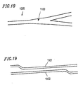
- a directional coupler using the effect of weak coupling of light between two waveguides 1901 and 1902 formed close to each other in parallel is also known (H. Nishihara et al., "Optical integrated circuit", Ohm, 1965, pp. 45-47, 51-54, and 266-267). (See Figure 19)
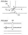
- FIG. 20A is a plan view of the element
- Figure 20B is a sectional view of the element taken along the line X-X' of Figure 20A.
- a deep groove (trench) 2002 is formed at a crossing 2001 of waveguides by etching so as to change the refractive index locally and thus to effect partial reflection of light.
- a star coupler as shown in Figure 21 is well known as an optical integrated circuit element for light multi-branching which branches input light into eight parts.
- This star coupler has a structure combining the elements shown in Figure 18 in series.
- Another disadvantage of the directional coupler is that, since the allowable range of wavelengths for the element is as small as ⁇ 3 nm and that of operating temperatures is as small as ⁇ 5°C, a mechanism for suppressing the wavelength variation of a light emitting element in an optical integrated circuit element and a parts.
- This star coupler has a structure combining the elements shown in Figure 18 in series.
- GB-A-1 496 939 discloses an integrated optical control element according to the preamble of claim 1.
- the present invention concerns an integrated control element as specified in claim 1.
- the multilayer structure includes two or more layers having different refractive indices, each layer having a thickness given by: (2m + 1) ⁇ 0 /(4ncos ⁇ ), where ⁇ 0 is the wavelength of light in vacuum, ⁇ is the angle between the direction of light propagation and a normal onto a layer of the multilayer structure, n is the refractive index of the layer, and m is an integer larger than 0.
- the mode of the light incident on the multilayer structure from the first waveguide is a TM mode and the angle ⁇ is 45° or more.
- the present invention further provides an optical integrated circuit device comprising a plurality of optical elements in combination, wherein at least one of the plurality of optical elements is an integrated optical control element as defined above.
- the optical integrated circuit device further comprises a substrate, the plurality of optical elements being formed integrally on the substrate.
- the optical integrated circuit device further includes a multi-function laser for supplying light to the integrated optical control element, the laser outputting, in use, a plurality of coherent laser beams.
- the optical integrated circuit device is an optical integrated circuit device for coherent detection and further includes a laser for local oscillation for supplying light to the integrated optical control element.
- the optical integrated circuit device is an optical integrated circuit device for coherent detection and further includes a laser for local oscillation for supplying light to the integrated optical control element, and wherein local oscillation light and signal light are input from outside to the integrated optical control element including a plurality of waveguides, and the multilayer structure is directly formed on a waveguide end face in the integrated optical control element for guiding the signal light.
- the at least one integrated optical control element is a light demultiplexing element for dividing one input beam into a plurality of output beams.
- the optical integrated circuit device is an optical integrated circuit device for coherent detection and further includes a laser for local oscillation for supplying light to the integrated optical control element.
- the optical integrated circuit element further comprises a plurality of waveguides, and the multilayer structure is directly formed on a waveguide end face in the at least one integrated optical control element for guiding signal light input from outside.
- the first waveguide further includes a first upper cladding layer disposed above the first core layer, the first upper cladding layer having a smaller refractive index than the first core layer; wherein the second waveguide further includes a second upper cladding layer disposed above the second core layer, the second upper cladding layer having a smaller refractive index than the second core layer; and wherein a concave portion is defined between the first waveguide and the second waveguide, the concave portion extending through at least the first core layer and the first lower cladding layer.
- a multilayer structure is formed between a first waveguide and a second waveguide.
- the multilayer structure includes one or more layers with refractive indexes different from the equivalent refractive index of the surrounding region.
- the multilayer structure reflects or transmits light input from a first input waveguide.
- the reflected light and the transmitted light are coupled to second output waveguides.
- the size of the element can be as small as the width of the waveguides.
- the variation in reflectance is as small as ⁇ 1% for a large variation in wavelength used of about ⁇ 30 nm and a large variation in operating temperature of ⁇ 30°C.
- the element can operate stably even when the environment is not stable.
- the respective layers can control light efficiently.
- the refractive index and the thickness of the multilayer reflection film required for the control of the reflectance of the element is controllable with a precision of ⁇ 1% by the thin film formation process such as vapor phase crystal growth. Accordingly, the reflectance and transmittance of the element can be precisely controlled, and high production yield and reproducibility can be secured.
- the TM mode light is input to the multilayer reflection film, and the vertical end face of the first waveguide possibly forms an angle of about 45° with respect to the light proceeding direction. That is, the angle ⁇ formed by the light propagating direction in the first layer and the normal of the multilayer reflection film is 45°.
- the incident light is an S wave with respect to the end face, and therefore light dividing/coupling can be realized by the two output waveguides crossing at right angles.
- a multilayer reflection film is formed on a vertical end face of the first waveguide structure. Then, a second waveguide structure is formed in contact with the multilayer reflection film so that core layers of the two waveguide structures are positioned at substantially the same vertical level.
- a vertical end face is formed first by forming a concave structure on a substrate. Then, first and second waveguides are formed simultaneously. A multilayer reflection film is then formed on the vertical end face.
- the first and second waveguides are formed by the same process, they have the same structure.
- the refractive index and thickness of each layer, as well as the level of the vertical position of a core layer are identical between the first and second waveguides. Accordingly, the coupling efficiency between the first input waveguide and the second output waveguide can be improved.
- the invention described herein makes possible the advantages of (1) providing an integrated optical control element with a size of several micrometers square where the variation in optical coupling/dividing ratio (reflectance and transmittance) in response to a variation in operating temperature and light wavelength used is sufficiently small and the production yield and reproducibility of the element is high due to a large allowance of the optical coupling/dividing ratio with respect to the process precision, (2) a method for fabricating such an integrated optical control element, (3) an optical integrated circuit element using such an integrated optical control element, and (4) an optical integrated circuit device using such an integrated optical control element.
- FIGS 1A to 1C and 2A to 2C show steps of the fabricating process of the 2-beam laser device of this example.
- MOCVD metal organic chemical vapor deposition
- a diffraction grating 120 having a pitch of about 0.36 ⁇ m and a depth of about 0.18 ⁇ m is formed by nomal 2-flux interference exposure and wet etching.
- This diffraction grating 120 works as a third-order diffraction grating for laser light with a wavelength of 780 nm.
- the third-order diffraction grating is a grating which diffracts light so that the intensity of third-order diffraction light components of the diffracted light is the highest.
- the diffraction grating 120 is controlled to have a section ratio of a convex portion to a concave portion thereof of about 1:5.
- the stripe direction of the diffraction grating 120 is aligned in the [010] direction.
- a p-AlGaAs second cladding layer 106 with a thickness of 0.6 ⁇ m and a p-GaAs contact layer 107 with a thickness of 0.3 ⁇ m are formed on the resultant wafer with the diffraction grating 120 by MOCVD.
- a vertical step 131 is formed on the resultant wafer by normal photolithography and reactive ion etching using a dielectric film 130 as a Mask, so that a vertical face 132 is in the (010) plane. That is, the vertical face 132 and the stripe direction of the diffraction grating 120 form 45°.
- the height of the vertical step 131 is 3.0 ⁇ m, so that an etching bottom 133 reaches the GaAs substrate 100.
- an AlGaAs multilayer reflection film 109 using the dielectric film 130 as the mask, an AlGaAs multilayer reflection film 109, an AlGaAs lower cladding layer 110 with a thickness of 0.6 ⁇ m, an AlGaAs core layer 111 with a thickness of 0.8 ⁇ m, and an AlGaAs upper cladding layer 112 with a thickness of 1.0 ⁇ m are selectively formed by MOCVD.
- the multilayer reflection film 109 is composed of three sets of an Al 0.8 Ga 0.2 As layer with a thickness of 110 nm and an Al 0.1 Ga 0.9 As layer with a thickness of 83 nm, i.e., total six layers.
- the substrate surface (etching bottom) 133 formed by the etching is in the (100) plane, and the vertical face 132 is in the (010) plane. Accordingly, these two faces are crystallographically equivalent, meaning that a layer structure with a substantially equal thickness can be formed on both faces.
- the crystal growth temperature is set at a temperature in the range of 700°C to 750°C where the dependency of the crystal growth rate upon the plane orientation is smaller.
- All of the layers 109 to 112 formed in the selective crystal growth process are not doped with impurities so that they have high resistance.
- An unnecessary polycrystalline film (not shown) deposited on the dielectric film 130 in the above process is removed together with the dielectric film 130 by etching after the selective crystal growth process.
- the thus-fabricated wafer is composed of three sections, as shown in Figure 2B: a distributed feedback (DFB) type laser section 134; a demultiplexer section 135 including the multilayer reflection film 109 formed on the vertical face 132; and a passive waveguide section 136.
- a distributed feedback (DFB) type laser section 134 a laser section 134
- a demultiplexer section 135 including the multilayer reflection film 109 formed on the vertical face 132
- a passive waveguide section 136 a passive waveguide section 136.
- a stripe-shaped resistive electrode 140 is formed on the top surface of the laser section 134, while a resistive electrode 141 is formed over the entire bottom surface of the substrate 100.
- the stripe-shaped resistive electrode 140 has a width of 3 ⁇ m, and is arranged so that two strips in the ⁇ 011> and ⁇ 01-1> directions are perpendicular to each other near the multilayer reflection film 109.
- mesa stripes 142, 143, and 144 with a width of 3 ⁇ m and a height of 0.8 ⁇ m are formed on the thus-fabricated wafer by normal photolithography and wet etching.
- ridge waveguides are fabricated.
- the mesa stripes (waveguides) 143 and 144 are arranged so that they are on one line.
- the mesa stripe (waveguide) 142 and the mesa stripes 143 and 144 are perpendicular to each other and arranged to share the multilayer reflection film 109 formed on the vertical face 132.
- the mesa stripes 142 and 144 correspond to the stripe-shaped electrode 140 in the laser section 134.
- the thus-fabricated wafer is cleaved into chips.
- Each face of the chips is coated with a SiN reflection protection film (not shown) for suppressing the reflection of laser light, and thus the 2-beam laser device is completed.
- the laser section 134 of the laser element constitutes a DFB laser having the third-order absorption-type diffraction grating 120 along the waveguide 144, which emits laser light by applying a current between the electrodes 140 and 141.
- the DFB laser unlike a normal Fabry-Pérot laser, laser oscillation can be generated, without an end face mirror, by the effect of distributed feedback of light by the diffraction grating 120.
- Laser light generated by the DFB laser propagates through the waveguide 144 and is incident on the demultiplexer section 135 including the multilayer reflection film 109.
- the multilayer reflection film 109 constituting the demultiplexer section 135 is composed of three sets of the AlGaAs layer with a thickness d2 of 110 nm and the AlGaAs layer with a thickness d1 of 83 nm (total six layers).
- Incident light 20 input to the multilayer reflection film 109 from the DFB laser at an incident angle ⁇ is divided into reflection light 21 reflected in a 29 direction with respect to the incident direction and transmission light 22 passing through the multilayer reflection film 109 substantially straight.
- Figure 4 shows the dependency of the reflectance (and the transmittance which is 1 - reflectance) of the multilayer reflection film 109 upon the incident angle ⁇ .
- the characteristic obtained when light of the TM mode (the mode where the direction of the photoelectric field is vertical to the active layer 102) is incident from the DFB laser of the laser section 134 is shown by dotted lines, while the characteristic obtained when light of the TE mode (the mode where the direction of the photoelectric field is parallel to the active layer 102) is incident is shown by dash-dot lines.
- the incident angle ⁇ is 45° and the oscillation node of the DFB laser is the TM mode. Accordingly, the reflectance of 50% and the transmittance of 50% are obtained, and thus the incident light 20 is substantially equally divided into the reflection light 21 and the transmittance light 22.
- the allowable range of the angle ⁇ formed between the vertical face 132 and the direction of the mesa stripe 144 required to obtain the intensity ratio of the reflection light to the transmission light of 1:1 is 42° to 47°, which Is comparatively wide. Accordingly, high production yield can be ensured even when an unintended change occurs in the fabrication process. Further, since the multilayer reflection film 109 is formed by MOCVD, the refraction index of each layer of the film can be controlled with a precision of 1% or less. Accordingly, the uniformity, controllability, and the reproducibility of the reflectance and transmittance are high. The variations in reflectance and transmittance can be as small as the order of 50 ⁇ 0.4%.
- the incident angle e is 45°. Accordingly, the direction 2 ⁇ of the reflection light is vertical to the direction of the incident light. This means that the light from the waveguide 144 of the laser section 134 incident on and reflected from the multilayer reflection film 109 formed on the vertical face 132 enters the waveguide 142 formed in the direction perpendicular to the incident direction.
- the transmission light is input to the passive waveguide section 136 composed of the 3-layer structure formed together with the multilayer reflection film 109 (the lower cladding layer 110, the core layer 111, and the upper cladding layer 112) and the stripe structure (the mesa stripe 143).
- the core layer 111 of the passive waveguide section 136 is formed at a vertical position of substantially the same level as that of the active layer 102 of the laser section 134 where the peak of light exists.
- the light which has been emitted from the laser section 134 and passed through the demultiplexer section 135 is coupled to the passive waveguide section 136.
- a high coupling efficiency between the laser section 134 and the passive waveguide section 136 can be obtained by precisely controlling the depth of the etching at the formation of the vertical face 132 and the thickness of each layer at the selective crystal growth so as to allow the level of the vertical position of the center of the core layer 111 to be equal to that of the center cf the active layer 102.
- the precision of this equality is required to be ⁇ 0.3 ⁇ m.
- the same multilayer structure as the multilayer reflection film 109 of the demultiplexer section 135 formed on the vertical face 132 is formed on the substrate 100 in the fabrication process, which is located below the 3-layer structure in the passive waveguide section 136.
- the core layer 111 and the lower cladding layer 110 are made as thick as 0.8 ⁇ m and 0.6 ⁇ m, respectively, so that light guided by the passive waveguide 143 does not reach the multilayer reflection film 109 of the passive waveguide section 136, and thus the multilayer reflection film 109 does not adversely affect the waveguide mode of the waveguide 143.
- the demultiplexer section 135 which includes the multilayer reflection film 109 and has no waveguide mechanism. This allows the light to diverge due to a diffraction effect.
- the length of the demultiplexer section 135 is only about 2 ⁇ m, the element characteristic is not so significantly affected by this section.
- light of substantially the same amount as the light obtained when the two waveguides 143 and 144 are in direct contact specifically, about 95% of the light obtained when the two waveguides are in direct contact, couples to the passive waveguide 143.
- the length of the demultiplexer section 135 is required to be 5 ⁇ m or less.
- the two light beams separating at the multilayer reflection film 109 in the demultiplexer section 135 are coupled to the waveguides 142 and 143, propagate therethrough, and are output from the respective end faces.
- the laser light is also output backward from the end face of the waveguide 144 of the laser section 134 due to the structure of the laser element.
- laser light is output in the total of three directions from one laser resonator.
- the light output backward is received by a light receiving element disposed near the element and used for light amount monitoring.
- the regaining two output light beams are output outside the element, keeping the coherence between each other.
- the laser element is thus used as a coherent 2-beam laser source.
- Figure 5 shows the dependency of the reflectance of the multilayer reflection film 109 having the above structure upon the laser light wavelength.
- the laser wavelength used in the 2-beam laser device of Example 1 is 850 nm, and the element is controlled so that both the reflectance and the transmittance are 50% at this wavelength.
- the variation in wavelength generally about ⁇ 1 nm
- a variation in oscillation wavelength generally about ⁇ 2 nm for a DFB laser
- the variation in reflectance of the element is minor, which is in the range of 50% ⁇ 0.3%. Accordingly, the element of Example 1 does not require a control system for strictly keeping the wavelength of the used laser light at a fixed value.
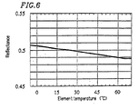
- Figure 6 shows the dependency of the reflectance of the multilayer reflection film 109 with the above structure upon the element temperature.
- the temperature of the element of Example 1 varies in the range of -5°C to 70°C which is a temperature range generally allowable for home appliances, the reflectance of the element varies only in the range of 49% to 51%. Accordingly, the element of Example 1 does not require temperature control in the above temperature range. It does not need to monitor the output light power from a demultiplexer and conduct feedback control of the operation conditions of the demultiplexer based on the results of the monitoring by use of an external circuit, either.
- Figure 7 shows the variation in reflectance when the thickness of the multilayer reflection film 109 varies from the set value.
- the controllability of the film thickness of about ⁇ 3% should be secured at the second selective crystal growth by MOCVD in the above-described fabrication method. It is well known that the crystal growth by MOCVD allows the film thickness to be controlled at a precision of ⁇ 1% or less for both the distribution in one wafer and the variation among wafers. The experimental results by the Inventors have confirmed that the film thickness on the vertical face can also be controlled at the same level of precision.
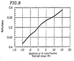
- Figure 8 shows a variation in reflectance when the Al mole fraction of the layers of the multilayer reflection film varies from the above set value.
- the controllability of the Al mole fraction of about ⁇ 1% should be secured at the second selective crystal growth by MOCVD in the above-described fabrication method. This condition can be fully satisfied by the controllability of the Al mole fraction obtained by the MOCVD method. Accordingly, the controllability and the reproducibility in the fabrication of the multilayer reflection film are satisfactorily high, and thus high production yield can be obtained.
- the 2-beam laser device of Example 1 is applicable as the light source for various laser interference measurement systems such as a laser speedometer and a laser distance measuring device.
- one output light beam emitted from a conventional laser is divided into two by an external demultiplexer. This makes the configuration of the resultant optical system complicated and large in many cases. Also, the adjustment of the optical system is difficult.
- the optical structure can be made simple and small, and thus the adjustment thereof can be made simple and easy.
- Example 2 the integrated optical control element is applied to a coherent detection element.
- Figures 9A to 9C and 10A to 10C the structure and the fabrication method of the coherent detection element of Example 2 will be described.
- Figures 9A to 9C and 10A to 10C show the steps of the fabrication process of the coherent detection element.
- an n-InGaAs first etching stop layer 301 with a thickness of 0.01 ⁇ m and an n-InP buffer layer 302 with a thickness of 1.0 ⁇ m are formed on an n-InP substrate 300 by molecular beam epitaxy using organic metal material (MOMBE).
- MOMBE organic metal material
- a diffraction grating 320 having a pitch of 220 nm and a depth of 70 nm is formed on the buffer layer 302 by normal photolithography using a 2-flux interference exposure method and wet etching.
- a region of the above multilayer structure is etched to reach some level of the n-InP buffer layer 302 by normal photolithography and reactive ion beam etching.
- a patterned SiN film 330 is used as a mask. The etching conditions are controlled so that a vertical etching face can be obtained.
- the remaining portion of the n-InP buffer layer 302 is removed by a hydrochloric acid etchant to reach the first etching step layer 301, and then the first etching stop layer 301 is removed by a sulfuric acid etchant.
- the etching face can be made vertical by the reactive ion beam etching and simultaneously the selective etching can be obtained by wet etching. That is, the etching face vertical to the substrate 300 and a surface 331 of the substrate 300 are exposed.
- the etching depth can be equal to the total of the thicknesses of the layers 301 to 308.
- a vertical face 332 forming 45° with regard to the grooves of the diffraction grating 320 and a vertical face 333 forming 90° with regard to the grooves of the diffraction grating 320 are formed simultaneously in the etching process.
- the two vertical faces 332 and 333 thus form an angle of 45°.
- the multilayer reflection film 309 is composed of two sets of an InP layer (active to a wavelength of 1.45 ⁇ m) with a thickness of 173 nm and an InGaAsP layer (active to a wavelength of 1.45 ⁇ m) with a thickness of 159 nm (total four layers).
- the thicknesses of the InP layer and the InGaAsP layer on the vertical face 332 are set to satisfy ⁇ 2 ⁇ 0 /(4 ⁇ n) where ⁇ 0 is the wavelength of light passing through the multilayer reflection film 309 in vacuum, and n is the refractive index of each layer constituting the multilayer reflection film 309.
- an ohmic electrode 340 with a width of 3 ⁇ m is formed on the p-contact layer 308 and an ohmic electrode 341 is formed over the entire bottom surface of the substrate 300.
- mesa stripes 350 to 353 crossing at right angles at the multilayer reflection film 309 formed on the vertical face 332 are formed by normal photolithography and selective etching. Specifically, first, using an organic resist as a mask, unmasked portions are etched to a depth of about 0.9 ⁇ m from the wafer surface by ion etching. Then, only the remaining InP layers are removed by a hydrochloric acid etchant to expose the InGaAs etching stop layers 306 and 313.
- the thicknesses of the cladding layer 305 and the upper cladding layer 312 located above the waveguide layers (the guide layer 303, the active layer 304, and the core layer 311) on the sides of the mesa stripes 350 to 353 can be strictly controlled.
- the transverse mode characteristic of the waveguide defined by the mesa stripes 350 to 353 can be controlled with high precision.
- the thus-fabricated wafer is cut into chips.
- the faces of each chip are coated with a reflection prevention film (not shown) made of a dielectric film, and thus the coherent detection element is completed.
- the function of the element of Example 2 is to divide light from each of the input waveguides (mesa stripes) 350 and 353 into two beams, and simultaneously couple each one beam from one of the input waveguides with each one beam from the other input waveguide.
- the coupled beams are then input to the output waveguides (mesa stripes) 351 and 352.
- the input waveguide 350 constitutes a distributed feedback laser (DFB-LD), which emits laser light (corresponding to local oscillation light) with a wavelength of 1.55 ⁇ m when a current flows between the electrodes 340 and 341.
- DFB-LD distributed feedback laser
- TM mode light is provided with a larger optical gain than TE mode light.
- the thus-generated local oscillation laser light having the TM mode propagates through the input waveguide 350 and incident on the multilayer reflection film 309 formed on the waveguide face (vertical face) 332 formed vertical to the substrate 300.
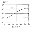
- Figure 11 shows the variation in light intensity reflectance when TM mode light is input to the multilayer reflection film 309 at an incident angle of 0° to 60°.
- the multilayer reflection film 309 works as a semi-transparent film with a reflectance of 10% and a transmittance of 90%.
- the light passing through the multilayer reflection film 309 is then input to the output waveguide 351 formed close to the multilayer reflection film 309 and propagates in the output waveguide 351.
- Light reflected from the multilayer reflection film 309 proceeds in a direction vertical to the input waveguide 350 and is input to the multilayer reflection film 309 formed on the vertical face 333 vertical to the light proceeding direction.
- the incident angle at this time is 0° (parallel to the normal of the face).
- light is little reflected when input at the incident angle of 0° (the reflectance is less than 0.1%). Accordingly, light is little influenced by the multilayer reflection film 309 on the vertical face 333, and passes therethrough to be input to the output waveguide 352.
- the light emitted from the input waveguide 350 is divided into two at the multilayer reflection film 309 on the vertical face 332 which forms a 45° angle with respect to the light proceeding direction, and the divided two beams are coupled to the output waveguides 351 and 352 each of which constitutes a passive waveguide composed of the layer structure formed in the second selective crystal growth process.
- signal light is input to the passive input waveguide 353, and then input to the multilayer reflection film 309 formed on the vertical face 332 at an incident angle of 45°, as in the case of the local oscillation light.
- 10% of the incident light is reflected to be input to the output waveguide 351, while 90% thereof passes through the multilayer reflection film 309 so as to be coupled to the output waveguide 352.
- the multilayer reflection film 309 formed on the vertical face 332 divides each of the local oscillation light and the signal light into two and simultaneously couples these two different types of light.
- the coupled signal light and local oscillation light propagate in the output waveguides 351 and 352 to reach the end faces thereof, and are then output from the end faces.
- the two output beams are converted into electric signals by respective high-speed light receiving elements (not shown) separately disposed, and resultant signals are demodulated by a signal processing circuit.
- coherent detection can be realized.
- the area occupied by the integrated optical control element can be as small as about W 2 (where W is the width of the waveguide).
- W is the width of the waveguide.
- the size of the integrated circuit element for coherent detection can be made as small as 1 mm 2 or less.
- the variation in reflectance when the operating temperature of the element varies in the range of 0°C to 60°C is as small as ⁇ 0.2%. This eliminates the necessity of controlling the temperature of the element.
- the variation in reflectance when the light wavelength varies in the range of 1.3 ⁇ m to 1.7 ⁇ m is as small as ⁇ 0.4% or less. This makes it possible to use the element of the same structure for a system using the wavelength within the above range.
- Example 2 also, by using the incident angle dependency of the reflectance of the multilayer reflection film 309 shown in Figure 11, the output waveguide 352 which includes the multilayer structure formed in the second selective crystal growth process can be used as a passive waveguide.
- the waveguides 351 and 352 which allow the coupled light to propagate therein can be passive waveguides of the same structure. This reduces power consumption.
- Example 3 a modification of the element of Example 2 will be described.
- the reflectance of the multilayer reflection film 309 is preferably 50%.
- the element of Example 2 is modified to have a multilayer reflection film consisting of more layers though the modified element is not shown.
- the multilayer reflection film of Example 3 is composed of five sets of the InGaAsP layer and the InP layer (total ten layers) each of which has the same thickness as that of the multilayer reflection film 309. The reflectance of 50% can be obtained by this structure.
- the entire thickness of the multilayer reflection film of this example increases to 1.66 ⁇ m due to the increase in the number of layers.
- the etching depth at the formation of the vertical face should be increased accordingly. That is, the n-type cladding layer 302 constituting the laser should be thickened accordingly.
- Example 3 as in Example 2, a small-size integrated optical control element with high stability against the variations in operating temperature and wavelength used can be realized. Also, good production yield and reproducibility of the element can be obtained.
- Example 4 another modification of Example 2 for obtaining the light coupling/dividing ratio of 1:1 (reflectance: 50%) will be described.
- FIG. 4 is a top view showing the waveguides and the multilayer reflection film of the integrated optical control element of Example 4.
- a multilayer reflection film 509 is composed of two sets of an InGaAsP layer with a thickness of 0.31 ⁇ m and an InP layer with a thickness of 0.29 ⁇ m (total four layers).
- the element is arranged so that the normal of the multilayer reflection film 509 forms a 67° angle with respect to both local oscillation light output from a waveguide 550 corresponding to the DFB-LD and signal light input from outside the element and propagating in a passive waveguide 553.
- the waveguide 553 and a waveguide 552 are formed to be vertical to the cleaved surface of the element because the DFB-LD does not need waveguide end face reflection and the input waveguide 553 should desirably have an input end face substantially vertical to the waveguide in order to receive light from outside.
- the reflectance of 47% can be obtained by the multilayer reflection film 509 composed of only four layers, and thus the coupling/dividing ratio of 1:1 can be obtained.
- the element with a size of 1 mm 2 the local oscillation light and the signal light propagating in the input waveguides 550 and 553, respectively, can be divided/coupled at the ratio of 1:1, and the coupled light can be coupled to output the waveguides 551 and 552 so as to be output from the element.
- the element of Example 4 also has high stability against the variations in operating temperature and wavelength used, and the operable ranges for the temperature and the wavelength as wide as those in Examples 1 and 2 can be secured.
- the reflectance varies largely with the variation in the angle of the multilayer reflection film 509 with respect to the waveguide direction.
- the reflectance varies by ⁇ 3% or more with the variation in the angle by ⁇ 1°.
- the angle should be controlled with a precision of ⁇ 0.2° or less at the formation of the vertical face prior to the formation of the multilayer reflection film 509. Since the above precision directly relates to the masking precision in normal photolithography, it is easy to control the angle at a precision of ⁇ 0.2° or less.
- the angle of the vertical face (the incident angle), as well as the film thicknesses and the mole fraction of each layer of the multilayer reflection film 509, can be satisfactorily controlled to realize the element of this example, and thereby high production yield and reproducibility are secured.
- Example 5 an element having substantially the same structure as that of Example 1 is fabricated by a different fabrication method.
- Figures 13A, 13B, 14A, and 14B show the steps of the fabrication process of the element of this example.
- an undoped Al 0.25 Ga 0.75 As lower cladding layer 601 with a thickness of 0.7 ⁇ m, an Al 0.2 Ga 0.8 As core layer 602 with a thickness of 0.3 ⁇ m, and an undoped Al 0.25 Ga 0.75 As upper cladding layer 603 with a thickness of 0.6 ⁇ m are formed on a semi-insulating GaAs substrate 600 having the (100) plane by molecular beam epitaxy (MBE).
- MBE molecular beam epitaxy
- An SiO 2 film with a thickness of 0.3 ⁇ m is formed on the resultant wafer surface by sputtering, and then a right-angled equilateral triangle shaped portion of the SiO 2 film is etched by normal photolithography and etching using a hydrofluoric acid etchant.
- the length of the two equal sides forming a right angle is 4 ⁇ m, and the two equal sides extend in the ⁇ 01-1> and ⁇ 011> directions while the remaining side extends in the ⁇ 001> direction.
- a concave structure 610 is formed by reactive ion beam etching using chloride gas so that the bottom of the structure reaches the GaAs substrate 600.
- the etching depth is about 2 ⁇ m.
- a multilayer reflection film 620 composed of two sets of an AlAs layer and a GaAs layer (total four layers), and an Al 0.25 Ga 0.75 As burying layer 621 with a thickness of 1.5 ⁇ m are consecutively formed by MOCVD selective growth.
- the multilayer reflection film 620 has a thickness which satisfies expression (1) below at the portion thereof formed on the vertical face 611 which forms a 45° angle with respect to the light proceeding direction.
- ⁇ 0 is the wavelength of light in a vacuum (1.3 ⁇ m)
- ⁇ is the angle formed by the light proceeding direction and the normal of the layer (45°)
- n is the refractive index of the layer for 1.3 ⁇ m wavelength light
- m is an integer more than 0.
- Figure 14A is a sectional view of the wafer shown in Figure 13B taken along the line A-A' of Figure 13B.
- the concave structure 610 is completely buried, so that the surface of the resultant wafer is substantially flat.
- a T-shaped mesa stripe 630 extending in the ⁇ 01-1> and ⁇ 011> directions which are perpendicular to each other is formed by normal photolithography and wet etching.
- the mesa stripe 630 has a width of 3 ⁇ m and a height of 0.4 ⁇ m.
- the mesa stripe 630 is formed so that the crossing of the two bars of the T shape corresponds to the position of the multilayer reflection film 620 formed on the vertical face 611. Ridge waveguides 631, 632, and 633 are formed from the mesa stripe 630.
- the resultant wafer is cleaved into chips, and three waveguide end faces of each chip are coated with anti-reflection coating film made of Si 3 N 4 (not shown) by the plasma chemical vapor deposition (P-CVD) method.
- P-CVD plasma chemical vapor deposition
- an integrated optical control element for light branching is fabricated.
- this element light output from a fiber and/or a laser diode is input to the input waveguide 631 at the end face thereof, and divided into two at the multilayer reflection film 620 , so as to be coupled to the output waveguides 632 and 633.
- the light output from the element is input to a fiber again.
- Example 5 light which has propagated through a fiber with a wavelength of 1.3 ⁇ m is coupled to the input waveguide 631 and then divided equally. The divided two beams are output from the element and coupled to two fibers.
- the size of the concave structure 610 including the multilayer reflection film 620 having the light branching function is 5 ⁇ m 2 or less.
- the entire element can be as small as 250 ⁇ m 2 .
- a light branching ratio of substantially 1:1 can be obtained.
- the variation in reflectance or transmittance is only about ⁇ 2% for the variation in wavelength of ⁇ 0.1 ⁇ m and the variation in operating temperature of ⁇ 40°C. Thus, very stable characteristics can be obtained.
- the input waveguide 631 and the two output waveguides 632 and 633 have the same layer structure formed in the same crystal growth process. Accordingly, the refractive index and the thickness of each layer and the level of the vertical position of the core layer 602 of the input waveguide 631 are identical to those of the output waveguides 632 and 633. This makes it possible to have a coupling efficiency as high as 95% between the input waveguide 631 and the output waveguides 632 and 633.
- the expanse of light due to light diffraction at the Al 0.25 Ga 0.75 As burying layer 621 where no waveguide structure exists can be negligibly small by reducing the length of this portion to 3 ⁇ m or less.
- the optical loss of the entire element including the waveguide loss (which becomes smaller as the size of the element is smaller) can be 1.5 dB or less.
- Example 6 an optical integrated circuit element for multi-branching applying the element of Example 5 will be described.
- the element of this example divides one input light signal into eight equal light signals.
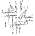
- Figure 15 is a top view showing the configuration of the optical integrated circuit element of Example 6.
- Each triangle mark in Figure 15 shows the concave structure 610 including the multilayer reflection film 620 of the integrated optical control element described in Example 5.
- Light input to the end face of an input waveguide 700 from a fiber 712 via a lens 711 is divided into two in power as the light passes through each of integrated optical control elements 710.
- the integrated optical control element 710 divides the power of input light into two equally at the multilayer reflection film thereof.
- the two divided beams respectively pass through three integrated optical control elements, and finally eight light signals having the same power are output to eight output waveguides 701 to 708.
- the eight light signals are then output to fibers through lenses.
- the size of the integrated optical control element 710 is about 5 ⁇ m 2 . Accordingly, the size of the entire element is restricted by the position of the outlets of the device connecting to fibers. In Example 6, since each two outputs are allocated on the four faces, the size of the entire package can be as small as 30 mm 2 . Since the branching characteristic (reflectance and transmittance) with respect to the variations in operating temperature and wavelength is stable, the operation of the optical integrated circuit element itself is stable against the variations in temperature and wavelength.
- the element of Example 6 can be applied as an element (passive demultiplexer) for an optical communication system in the case where communication is conducted by use of one fiber between a plurality of users by the time-division multiplex communication system and in the case where the same signal is distributed to a plurality of users as in cable broadcasting.
- Example 7 An integrated optical control element is fabricated by one thin film formation process.
- Figure 16 is a sectional view of the element of Example 7. Referring to Figure 16, the fabrication method of the element will be described.
- a concave portion 810 with a right-angled equilateral triangle shape as is viewed from top is formed on a glass substrate 800 by normal photolithography and dry etching.
- the shape of the concave portion 810 viewed from top is the same as that of Example 5.
- the concave portion 810 has a vertical face 811 which is to form 45° with respect to the light proceeding direction (corresponding to the oblique side of the right-angled equilateral triangle) and vertical faces 812 and 813 (corresponding to two sides perpendicular to each other).
- the length of the two sides perpendicular to each other is 4 ⁇ m
- the depth of the concave portion 810 is 2.8 ⁇ m.
- an SiO 2 buffer layer 801 with a thickness of 0.3 ⁇ m, an Si 3 N 4 core layer 802 with a thickness of 0.2 ⁇ m, an SiO 2 cladding layer 803 with a thickness of 0.5 ⁇ m, and a multilayer reflection film 804 are consecutively formed on the substrate 800 by P-CVD.
- the multilayer reflection film 804 is composed of three Si 3 N 4 layers and three SiO 2 layers and has a thickness satisfying expression (2) below, as in Example 5.
- ⁇ c is the wavelength of light in a vacuum (800 nm)
- ⁇ is the angle formed by the light proceeding direction and the normal of the layer (45°)
- n is the refractive index of the layer for 800 nm wavelength light
- m is an integer more than 0.
- the multilayer reflection film 804 with the thickness satisfying equation (2) can be formed on the vertical faces 811 and 812.
- an SiO 2 burying layer 805 is formed on the entire surface of the wafer by spin coating so as to have a thickness of 0.3 ⁇ m at the flat portion.
- mesa stripes i.e., waveguides are formed by normal photolithography and ion etching.
- Figure 16 is a sectional view of the portion of the element where the mesa stripe is formed, taken along the length of the mesa stripe.
- the waveguides form a cross shape crossing at the portion where the multilayer reflection film 804 is formed.
- the wafer is cut by a diamond blade to form the element.
- the cut faces should be substantially perpendicular to the waveguides so that the aligning with fibers at light inputs/outputs can be easy.
- Light with a wavelength of 800 nm is input to an input waveguide 820 of the thus-fabricated element.
- the light propagating through the input waveguide 820 is input to the multilayer reflection film 804 formed on the vertical face 811 at an incident angle of 45°. Part of the light is reflected from the multilayer reflection film 804.
- the remainder of the light which has passed through the multilayer reflection film 804 then passes through the SiO 2 burying layer 805 and reaches the multilayer reflection film 804 formed on the vertical face 812.
- the reflectance of light input to the multilayer reflection film 804 perpendicularly is less than 0.1%. Accordingly, light is little reflected from the multilayer reflection film 804 formed on the vertical face 812, and most of the light is coupled to an output waveguide 821.
- the light reflected from the multilayer reflection film 804 formed on the vertical face 811 forming 45° with respect to the light proceeding direction proceeds in a direction perpendicular to the plane of Figure 16, and is coupled to an output waveguide not shown.
- the basic structure used for the light branching/coupling is the multilayer reflection film composed of dielectrics, which can be formed in an area as small as 3 ⁇ m 2 .
- the entire element can be as small as 200 ⁇ m 2 .
- the branching/coupling ratio can be kept at 1:1 with a precision of ⁇ 1% for the variation in operating temperature of ⁇ 30°C and the variation in wavelength of ⁇ 50 nm.
- the entire size of the element including a package can be made small.
- the input waveguide 820, the output waveguide 821, and an output waveguide not shown which is located perpendicular to the plane of Figure 16 have the same waveguide structure formed in the same thin film formation process and the vertical positions thereof are at the same level.
- the light coupling efficiency between the input waveguide and the output waveguides can be as high as 95%. This makes it possible to suppress the light loss at the integrated optical control element of this example to 1.2 dB or less.
- the light branching/coupling element composed of the passive waveguides can be fabricated by one thin film formation process. Accordingly, the element fabrication process can be simplified, the production yield of the element can be further improved, and the production yield of the optical integrated circuit element using the element of this example can be improved.
- Example 8 an element integrating a laser element and a waveguide type light receiving element will be described.
- Figure 17 is a plan view of the element of Example 8.
- the basic structure of the element of this example is the same as that of Example 2. Accordingly, in Figure 17, components similar to those in Example 2 are denoted by the same reference numerals as those in Figures 9A to 9C and 10A to 10C.
- the element of Example 8 is different from the element of Example 2 in the structure of layers 309 to 314 corresponding to the waveguide structure formed at the second crystal growth.
- the structure is composed of an iron-doped semi-insulating multilayer reflection film 309, a p-In? lower cladding layer 310, a p-InGaAs core layer 311 having a composition absorbing laser light, an n-type InP first upper cladding layer 312, an n-type InGaAs third etching stop layer 313, and an n-InP second upper cladding layer 314.
- the thickness of each layer is the same as that in Example 2.
- N-type ohmic electrodes 951 and 952 are formed on output waveguides (mesa stripes) 351 and 352.
- a zinc diffusion region reaching the p-type lower cladding layer 310 is formed on a portion of the wafer where the mesa stripes are not formed, and a p-type ohmic electrode 953 is formed on the zinc diffusion region.
- the operation principle of the thus-fabricated element will be described.
- Light of the TM mode is input to the multilayer reflection film 309 from an input waveguide 350 constituting a DFB laser at an incident angle of 45°.
- signal light introduced to an input waveguide 353 from outside is input to the multilayer reflection film 309 at an incident angle of 45°.
- the length of the input waveguide 353 in the light propagating direction is preferably as small as possible because the input waveguide 353 constitutes a light receiving element and thus has large light absorption. In this example, it is 40 ⁇ m. This value is determined in consideration of the reliability of the input waveguide (laser portion) 350.
- the light incident on the multilayer reflection film 309 is branched/coupled according to the reflectance shown in Figure 11 and introduced to the output waveguides 351 and 352 which form a wavelength type light receiving element.
- the output waveguides 351 and 352 are electrically isolated from the laser portion 350 by the semi-insulating multilayer reflection film 309, and a reverse bias voltage can be applied between the electrodes 951 and 953 and between the electrodes 952 and 953. This makes it possible to realize a light receiving element with high-speed response.
- a signal with a beat frequency of 5 GHz corresponding to the frequency difference between the signal light and the local oscillation light can be detected.
- the output waveguides 351 and 352 are used as a light receiving element capable of being independently driven. Accordingly, in addition to the effect described in Example 2, the coherent detection function can be performed only by this element. This eliminates the necessity of disposing a light receiving element outside the element by aligning it with the element as in Example 2. Thus, the coherent detection system can be simplified and made small.
- Example 9 an integrated optical control element where both a waveguide structure and an optical control structure (layer) are formed by one thin film formation process will be described.
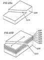
- a vertical step 2210 is formed on a (001) GaAs substrate 2200 by photolithography and dry etching.
- the direction of the step 2210 is set at the [010] direction so that the vertical face of the vertical step 2210 is substantially in the plane (010).
- the height of the step 2210 is set at 2.0 ⁇ m by controlling the etching time.
- the conditions are set as follows:
- the substrate temperature is as low as 600°C to 680°C;
- the mole ratio of the III-group atoms to the V-group atoms in the vapor is as large as 130 to 250; and the migration distance of adsorbed atoms or molecules on the crystal surface is short.
- a T-shaped mesa stripe 2211 with a width of 3.0 ⁇ m and a height of 4.0 ⁇ m is formed by normal photolithography and dry etching using an Si 3 N 4 film (not shown) as a mask.
- the mesa stripe 2211 is formed so that the crossing of two bars of the T shape corresponds to the position of the step 2210.
- an Al 0.25 Ga 0.75 As burying layer 2208 with a thickness of 4.0 ⁇ m is selectively formed so as to bury the portions other than the T-shaped mesa stripe 2211.
- the wafer is cleaved to form an element having four faces including three faces corresponding to the light input/output faces 2220 to 2222 as shown in Figure 23A.
- the thus-fabricated element includes a first waveguide 2212 composed of the first lower cladding layer 2201, the first core layer 2202, and the first upper cladding layer 2203 and a second waveguide 2213 composed of the second lower cladding layer 2205, the second core layer 2206, and the second upper cladding layer 2207.
- the second waveguide 2213 is put on the first waveguide 2212 in the layer thickness direction via an optical control layer 2204.
- Figure 23B is a partial sectional view of the element taken along the line B-B' of Figure 22B showing the portion at and around the vertical step 2210.
- signal light with a wavelength of 780 nm is input to the second waveguide 2213 composed of the second lower cladding layer 2205, the second core layer 2206, and the second upper cladding layer 2207, and propagates in the second waveguide 2213.
- the light propagating in the second waveguide 2213 then reaches the vertical step 2210. Due to the vertical bend of the second core layer 2206, the light enters the second lower cladding layer 2205 and then enters the optical control layer 2204 interposed between the second lower cladding layer 2205 and the first upper cladding layer 2203. Since the optical control layer 2204 has a step portion substantially corresponding to the vertical step 2210, the light is input to the optical control layer 2204 at an incident angle of about 45°.
- the light reflected from the optical control layer 2204 proceeds in a direction turned by 90° (direction vertical to the plane of Figure 23B). It propagates in the second waveguide 2213 again and is output outside the element from a sub-output end face 2221.
- the light which has passed through the optical control layer 2204 is coupled to the first waveguide 2212 including the first core layer 2202 as the center. After having propagated through the first waveguide 2212, the light is output outside the element from a main output end face 2222.
- the height of the step 2210 (2.0 ⁇ m) and the total thickness of the first core layer 2202, the first upper cladding layer 2203, the optical control layer 2204, and the second lower cladding layer 2205 are controlled under the conditions that the structures of the first waveguide 2212 and the second waveguide 2213 are the same and that the vertical positions of the first core layer 2202 and the second core layer 2206 are at the same level with a precision of the thickness of the core layer 2202 or 2206 or less.
- the light radiation loss at the optical coupling from the second waveguide 2213 to the first waveguide 2212 can be as small as about 3.0 dB or less.
- the light radiation loss at the optical coupling from the second waveguide 2213 to the first waveguide 2212 can be further as small as 1.0 dB or less.
- the light multi-reflection effect in the optical control layer 2204 is utilized for the reflectance and transmittance. Accordingly, the variation in reflectance and transmittance with the variation in temperature in the range of 0 to 60°C and the variation in wavelength in the range of 770 to 790 nm can be as small as ⁇ 1%. Thus, the variation in intensity of light output from the sub-output end face 2221 can be stabilized within ⁇ 1%. Further, the variation in reflectance and transmittance is as small as about ⁇ 1% for the variation in layer thickness and mole fraction by ⁇ 5% in the MOCVD crystal growth process. This allows for a sufficiently large allowance for the fabrication process. As a result, high reproducibility at the fabrication of the element and a production yield as high as 99% or more were obtained.
- the major portion of the element is the optical control layer 2204, the first waveguide 2212, and the second waveguide 2213 located at and around the vertical step 2210.
- the size of this region is determined by the width of the waveguides. In this case, it is as small as 3.0 ⁇ m 2 .
- Example 10 an integrated optical control element for coherent detection will be described with reference to Figures 25A, 25B, 26A, and 26B.
- a waveguide portion of the element is fabricated as follows. As shown in Figure 25A, an n-Al 0.5 Ga 0.5 As first cladding layer 2301 with a thickness of 1.9 ⁇ m, an Al 0.3 Ga 0.7 As core layer 2302 with a thickness of 0.3 ⁇ m, an Al 0.5 Ga 0.5 As second cladding layer 2303 with a thickness of 0.45 ⁇ m, a GaAs etching stop layer 2304 with a thickness of 3 nm, and an Al 0.5 Ga 0.5 As third cladding layer 2305 with a thickness of 0.45 ⁇ m are consecutively formed on an n-GaAs substrate 2300 by MOCVD, for example.
- a patterned dielectric film 2306 is formed on the resultant wafer.
- the above layers are selectively etched by normal reactive ion dry etching, leaving part of the first cladding layer 2301 as a thin layer.
- a V-shaped face 2307 formed by dry etching stand at 90° ⁇ 1° with respect to the surface of the core layer 2302. The etching depth is 2.6 ⁇ m with a precision of ⁇ 0.1 ⁇ m.
- a laser section for local oscillation light is fabricated as follows.
- a semiconductor multilayer reflection film 2308 is formed on the first cladding layer 2301 exposed by the above dry etching by the MOCVD crystal growth technique.
- the multilayer reflection film 2308 is composed of three sets of an n-Al 0.18 Ga 0.82 As layer with a thickness of 84 nm and an n-Al 0.92 Ga 0.18 As layer with a thickness of 112 nm (total six layers).
- a diffraction grating is formed using the optical absorption layer 2312 and the optical guide layer 2311 by normal electron beam drawing and wet etching.
- the diffraction grating has a pitch of 0.13 ⁇ m and a depth of 0.12 ⁇ m, and functions as a first-order diffraction grating for 0.85 ⁇ m-wavelength light.
- the area ratio of the optical guide layer 2311 to the optical absorption layer 2312 at the section of the diffraction grating is set at 1:1.
- a p-AlGaAs fifth cladding layer 2313 with a thickness of 0.29 ⁇ m, a p-AlGaAs etching stop layer 2314 with a thickness of 3 nm, and a p-AlGaAs sixth cladding layer 2315 with a thickness of 0.45 ⁇ m are consecutively formed on the diffraction grating.
- a semiconductor film formed on the dielectric film 2306 is then removed by etching.
- the third cladding layer 2305 and the sixth cladding layer 2315 are etched by normal photolithography and wet etching so as to form mesa-shaped waveguides 2320 to 2323.
- the mesa portions should form an angle of 45° with respect to the larger portion of the V-shaped face 2307.
- an electrode 2316 is formed on the mesa portion of the laser section.
- a light signal is introduced to the waveguide 2320 from an end face 2319.
- the light signal is divided into two at a ratio of about 1:1 at the multilayer reflection film 2308 and input to the waveguides 2321 and 2322.
- the waveguides 2320, 2321, and 2322 have the same core thickness, this influence is not negligible.
- the coupling loss from the waveguide 2320 to the waveguide 2321 can be suppressed to about 5% because only the multilayer reflection film 2308 exists between the waveguides.
- the coupling loss from the waveguide 2320 to the waveguide 2322 is as large as about 1 dB because the fourth cladding layer 2309 with a thickness of 0.9 ⁇ m exists between the waveguides and the light largely diffracts during passing the long distance of the shaded portion as shown in Figure 26B.
- the coupling loss to the waveguide 2321 is about 1 dB, while that to the waveguide 2322 is about 2 dB.
- a coherent detection element with higher sensitivity can be obtained by having no light-diffracting layer between the end face for receiving signal light and light receiving elements (disposed at the light output end faces of the waveguides 2321 and 2322 though not shown).
- the above effect can also be obtained by the elements of the above examples, when the input waveguide for signal light and the waveguide connected to a light receiving element are connected without a structure interposed therebetween except for the multilayer reflection film as in this example.
- the laser section for local oscillation may not necessarily be formed integrally as in Example 10. Instead, a separate DFB laser and the like may be connected to the waveguide 2323 for coherent detection. The same effect as described above will be obtained by the this structure.
- Example 11 a 2 x 2 optical branching waveguide (an integrated optical control element) will be described.
- the above layers are selectively etched by a depth of 2.0 ⁇ m by normal reactive ion dry etching, leaving part of the first cladding layer 2401 as a thinner layer.
- a semiconductor multilayer reflection film 2406 composed of three sets of an Al 0.18 Ga 0.82 As layer with a thickness of 84 nm and an Al 0.82 Ga 0.18 As layer with a thickness of 112 nm in this order (total six layers) is formed.
- the order of the formation of the Al 0.18 Ga 0.82 As layer and the Al 0.82 Ga 0.18 As layer of the multilayer reflection film 2406 does not influence the reflection characteristic of the film.
- the Al 0.18 Ga 0.82 As layer is formed before the Al 0.82 Ga 0.18 As layer, and these layers are sequentially stacked. That is, the layer with the higher refractive index is formed before the layer with lower refractive index.
- mesa-shaped waveguides 2412 to 2415 are formed using the patterned dielectric mask as shown in Figure 27B. As in Example 10, the waveguides are formed so as to have an angle of 45° against the multilayer reflection film 2406.
- the multilayer reflection film 2406 has a reflectance of 50% for 0.85 ⁇ m-wavelength light incident thereon at 45°.
- the coupling efficiency of the waveguide 2413 to the waveguide 2412 is degraded when the fourth cladding layer 2407 is thick and the gap between the waveguides is large.
- the fourth cladding layer 2407 is thin, inconsistency in mode arises between the waveguides 2412 and 2413 due to influence from the semiconductor multilayer reflection film, degrading the coupling efficiency therebetween.
- the Inventors have set the thickness (T) of the fourth cladding layer to satisfy: 0.3 ⁇ M W ⁇ T ⁇ 2.1 ⁇ M W where MW is the mode expanse width of the O-order mode of the waveguide 2412 in a downward direction, which is the distance where the light power at the waveguide 2412 decreases from the peak value to a value of exp(-2) times the peak value.
- Figure 28A shows the coupling efficiency between the waveguides 2412 and 2413 when the thickness of the fourth cladding layer/MW is varied. As is observed from Figure 28A, high coupling efficiency is obtained when the above condition, 0.3 ⁇ MW ⁇ T ⁇ 2.1 ⁇ MW is satisfied.
- the Inventors decided that the layer with a lower refractive index of the multilayer reflection film 2406 should be in contact with the fourth cladding layer. It the layer with a higher refractive index of the multilayer reflection film 2406 is in contact with the fourth cladding layer, a coupling loss of about 5% to 15% arises.
- the reflectance may vary depending on the thickness of the fourth cladding layer 2407.
- This problem can be overcome by setting the thickness of the fourth cladding layer 2407 at or around a value obtained by expression (5): m ⁇ 0 / [ 2 n 2 ⁇ 1 ⁇ ( n 0 sin ⁇ / n 2 ) 2 ⁇ 1 / 2 ] where ⁇ 0 is the wavelength of light in a vacuum, n 0 is the refractive index of the core layer, n 2 is the refractive index of the fourth cladding layer, ⁇ is the angle formed by the light propagating direction in the core layer and the normal of the multilayer film, and m is an integer more than 0.
- Figure 28B shows the reflectance of light incident on the waveguide 2413 from the waveguide 2412 when the thickness of the fourth cladding layer is varied.
- Example 11 the levels of the vertical positions of the waveguides 2412 and 2413 are deviated by 0.1 ⁇ m.
- the vertical positions are not necessarily at the same level, but the two waveguides only should be arranged so that the centers of the modes thereof be located substantially at the same level.
- Example 12 an element with substantially the same structure as that of Example 5 is fabricated using another multilayer film fabrication process.
- MOCVD metal organic chemical vapor deposition
- a waveguide pattern as shown in Figure 29A is printed on the resultant wafer by normal photolithography.
- the second upper cladding layer 2505 is selectively etched by wet etching to reach the etching stop layer 2504 by wet etching, so as to form a ridge structure.
- This etching process can be easily conducted by wet etching using a hydrofluoric acid etchant.
- an SiO 2 film 2507 is formed on the resultant wafer to a thickness of about 0.5 ⁇ m by sputtering.
- a pattern for a concave portion where a multilayer film is to be formed is formed on the resultant wafer by photolithography and etching.
- the pattern width is 3.02 ⁇ m.
- the concave portion having vertical faces is formed by dry etching such as CAIBE (chemical assist ion beam etching) using Cl 2 gas.
- the concave portion is deep enough to reach the GaAs substrate 2500 as shown in Figure 30C which is a sectional view taken along the line a-a' of Figure 30B.
- an Al 0.22 Ga 0.78 As layer with a thickness of 0.1025 ⁇ m, an AlAs layer with a thickness of 0.395 ⁇ m, and an Al 0.22 Ga 0.78 As layer with a thickness of 0.103 ⁇ m are formed twice in this order inside the concave portion by normal-pressure MOCVD, for example, so as to form a multilayer film composed of a total of six layers.
- the concave portion has an unburied area with a width of about 1.07 ⁇ m.
- the unburied area is finally buried with a material having a refractive index which is equal to or less than that of the material used for the multilayer film and is larger than n 0 sin ⁇ (where no is the refractive index of the first core layer and ⁇ is the angle formed by the light propagating direction in the first core layer and the normal of the multilayer film).
- a material having a refractive index which is equal to or less than that of the material used for the multilayer film and is larger than n 0 sin ⁇ (where no is the refractive index of the first core layer and ⁇ is the angle formed by the light propagating direction in the first core layer and the normal of the multilayer film).
- n 0 sin ⁇ where no is the refractive index of the first core layer and ⁇ is the angle formed by the light propagating direction in the first core layer and the normal of the multilayer film.
- the refractive index of the final burying layer among the plurality of layers constituting the multilayer structure is made larger than n 0 sin ⁇ (where n 0 is the refractive index of the first layer and e is the angle formed by the light propagating direction in the first layer and the normal of the multilayer structure) and smaller than those of the other layers of the multilayer structure.
- n 0 is the refractive index of the first layer and e is the angle formed by the light propagating direction in the first layer and the normal of the multilayer structure
- a precision deviation in the fabrication process can be absorbed by the final burying layer.
- the final burying layer therefore has a variation in its thickness substantially equal to the size variation in the fabrication process. According to this layer structure, however, the variation in reflectance due to the variation in the thickness of the final burying layer can be suppressed.
- the refractive index of the thickest layer among the plurality of layers constituting the multilayer structure may be made larger than n 0 sin ⁇ and smaller than those of the other layers of the multilayer structure.
- the same effect as that described above can be obtained by appropriately controlling the thickness of the thickest layer in consideration of an expected variation in the fabrication process.
- Figure 31 shows the reflectance characteristic obtained when the layers in the concave portion are formed so as to obtain a reflectance of 50%.
- the solid line shows the case where a ZnSe layer is formed as the final burying layer.
- the dotted line shows the case where an Al 0.83 Ga 0.17 As layer is formed as the final burying layer.
- Tables 1A and 1B below show the structures of the former case and the latter case, respectively.
- the process margin width is doubled by using the low refractive index material as the final burying layer.
- Each layer of the multilayer structure in the concave portion should be formed so that the variation in reflectance with the variation in the thickness of the final burying layer falls within a desired reflectance range.
- the desired reflectance range should be set within a range where the variation in reflectance of the multilayer structure with the variation in the thickness of the final burying layer is small. This range corresponds to portions in the vicinity of peaks of a sinewave of the reflectance characteristic curve shown in Figure 31. In a range corresponding to slopes of the sinewave thereof, the variation in reflectance with the variation in thickness of the final burying layer is large.
- conditions under which each layer of the multilayer structure is formed for example, the thickness, are set so that the variation in reflectance of the multilayer structure with the variation in the thickness of the final burying layer falls within the reflectance range corresponding to the portions in the vicinity of the peaks.
- the thickness of the final burying layer in this case, 1.07 ⁇ m
- the deviation of the reflectance from a desired value can be suppressed to the range of 40% to 50%.
- Example 12 the effect obtained when the reflectance is set at 50% was described.
- the effect can also be obtained for any selected reflectance by selecting a material having a refractive index equal to or less than that of the material used for the multilayer film and larger than n 0 sin ⁇ .
- Example 13 the optical branching waveguide (integrated optical control element) of Example 11 is applied to an optical integrated circuit device.
- Figure 32 shows an optical integrated circuit device using a 2 ⁇ 2 optical branching waveguide 2700 for coherent detection shown in Example 11.
- a DFB laser 2702 is connected to a waveguide 2413 of the optical branching waveguide 2700 so that the laser light output end face of the DFB laser 2702 is in contact with the end face of the waveguide 2413.
- laser light (local oscillation light) from the DFB laser 2702 is introduced to the waveguide 2413.
- An optical fiber 2701 transmitting signal light is connected to and in contact with the end face of a waveguide 2414, so that the signal light is introduced to the waveguide 2414.
- the local oscillation light and the signal light are branched to waveguides 2412 and 2415.
- Light receiving elements (not shown) are disposed at the end faces of the waveguides 2412 and 2415 for coherent detection.
- Example 13 since the integrated optical control element can output light in any direction, the packaging of the optical element can be efficient compared with conventional elements. This makes it possible to reduce the size and weight of the optical integrated circuit device.
- Figure 33 shows an optical integrated circuit element of Example 14.
- the optical integrated circuit element of this example has an optical input 2802 composed of a tapered waveguide.
- An optical fiber 2800a is connected to this element via an external lens 2801. More specifically, a light intensity modulation signal transmitted from outside through the optical fiber 2800a is introduced to the optical integrated circuit element via the lens 2801.
- the optical input 2802 compcsed of a tapered waveguide provides an effect of minimizing the reduction of the coupling efficiency even when the positional relationship between the optical fiber 2800a and the waveguide portion of the optical integrated circuit element is deviated.
- the positional relationship is deviated by several micrometers by a temperature change even when the optical fiber and the waveguide are firmly fixed to each other.
- the reduction of the coupling efficiency can be prevented by having the tapered waveguide.
- the structure of such a tapered waveguide may have a structure described in A. Fenner Milton, et al., "Mode Coupling in Optical Waveguide Horns", IEEE, J.Q. EQE-13, p 828 (1977), for example.
- An optical amplifier 2803a is disposed downstream of the optical input 2802 for amplifying the signal light because the signal light input through the optical fiber 2800a becomes weak after long-distance transmission.
- the optical amplifier may have a structure described in Kitamura, et al., "Polarisation Insensitive Semiconductor Optical Amplifier Array grown by Selective MOVPE", 1993. Electronic Information Communication Association Fall Convention, 4-180, for example.
- An integrated optical control element 2804a is disposed downstream of the optical amplifier 2803a for dividing the signal light into two.
- An optical detector 2805 is disposed downstream of the integrated optical control element 2804a for converting one of the two beams divided by the integrated optical control element 2804a into an electric signal. The signal is used as a monitor for demodulating a data signal or maintaining the communication system.
- the other of the divided beams is sent to an optical amplifier 2803b for amplifying the beam which becomes weak by the division.
- the amplified beam is then divided into two by an integrated optical control element 2804b.
- One of the divided beams is output from the waveguide portion, converged by a microlens 2806, and then coupled to an optical fiber 2800b.
- the microlens may have a structure described in Shimada, et al., "Microlens fabricated by the Planner Process (V) - Integration with InP Laser Diode", The 55th Applied Physics Association Lecture Meeting Extended Abstract, p-908, for example.
- the other of the divided beams is again amplified by an optical amplifier 2803c, and then divided into two by an integrated optical control element 2804c.
- the two divided beams are converged by microlenses 2806 and then received by optical fibers 2800c and 2800d, respectively.
- the signal light received by the optical fibers 2800c and 2800d is transmitted to other optical integrated circuit elements (not shown), for example.
- Example 14 small-size integrated optical control elements with high stability against temperature change are used in combination with other optical elements, for example, passive waveguides such as external modulators, LEDs, and spot converters.
- passive waveguides such as external modulators, LEDs, and spot converters.
- the refractive index of the thickest layer of the multilayer structure may be made larger than n 0 sin ⁇ and smaller than those of the other layers.
- the same effect as that described above can be obtained by appropriately controlling the thickness of the thickest layer in consideration of an expected variation in the fabrication process.
Landscapes
- Physics & Mathematics (AREA)
- General Physics & Mathematics (AREA)
- Optics & Photonics (AREA)
- Engineering & Computer Science (AREA)
- Microelectronics & Electronic Packaging (AREA)
- Condensed Matter Physics & Semiconductors (AREA)
- Electromagnetism (AREA)
- Optical Integrated Circuits (AREA)
- Semiconductor Lasers (AREA)
Claims (11)
- Integriertes optisches Steuerelement mit:einem ersten Wellenleiter (2412,2415), in dem sich von außen einfallendes Licht ausbreiten kann;einer Multischichtstruktur (2406), auf die Licht, das sich im ersten Wellenleiter ausgebreitet hat, auftreffen kann und zum Übertragen des Lichtes oder Reflektieren des Lichtes, wobei die Multischichtstruktur wenigstens eine Schicht aufweist, die einen Brechungsindex hat, der verschieden ist vom entsprechenden Brechungsindex eines mit der einen Schicht in Kontakt stehenden Bereichs; undeinem zweiten Wellenleiter (2413, 2414) zum Empfangen von wenigstens einem Teil des von der Multischichtstruktur übertragenen oder reflektierten Lichtes;dadurch gekennzeichnet,dass jeder der ersten und zweiten Wellenleiter ein Rippen-Wellenleiter ist, in dem sich ausbreitendes Licht in einer lateralen Richtung des Wellenleiters eingeengt ist;dass der erste Wellenleiter eine erste Kernschicht (2402) aufweist, die im Betrieb einen Kern zum Führen des Lichtes darstellt und eine erste untere Mantelschicht (2401) unterhalb der ersten Kernschicht (2402) mit einem im Vergleich zur ersten Kernschicht kleineren Brechungsindex aufweist;dass der zweite Wellenleiter eine zweite Kernschicht (2408) und eine unterhalb der zweiten Kernschicht angeordnete untere Mantelschicht (2407) mit einem im Vergleich zur zweiten Kernschicht kleineren Brechungsindex aufweist;dass ein Teil der Multischichtstruktur (2406) unterhalb der zweiten unteren Mantelschicht (2407) angeordnet ist und ein Teil der ersten unteren Mantelschicht (2401) unterhalb des Teils der Multischichtstruktur (2406), der unterhalb der zweiten unteren Mantelschicht (2407) liegt, angeordnet ist;dass die Dicke der zweiten unteren Mantelschicht (2407) größer oder gleich des 0.3 und kleiner oder gleich des 2.1 fachen Abstands eingestellt wird, bei dem die Strahlintensität im ersten Wellenleiter von einem Maximalwert auf einen Wert des exp(-2) fachen des Maximalwerts in der ersten unteren Mantelschicht (2401) abgefallen ist.
- Integriertes optisches Steuerelement nach Anspruch 1, wobei die Multischichtstruktur (2406) zwei oder mehr Schichten mit verschiedenen Brechungsindizes aufweist und jede Schicht eine Dicke von

- Integriertes optisches Steuerelement nach Anspruch 2, wobei der Mode des von dem ersten Wellenleiter auf die Multischichtstruktur (2406) einfallenden Lichtes ein TM Mode ist und der Winkel Θ 45° oder mehr beträgt.
- Integrierte optische Schaltkreisvorrichtung mit einer Mehrzahl kombinierter optischer Elemente, wobei wenigstens eines der Mehrzahl der optischen Elemente einem in einem der Ansprüche 1 bis 3 definierten integrierten optischen Steuerelement entspricht.
- Integrierte optische Schaltkreisvorrichtung nach Anspruch 4 mit zusätzlich: einem Substrat, wobei die Mehrzahl der optischen Elemente auf dem Substrat integriert ausgebildet sind.
- Integrierte optische Schaltkreisvorrichtung nach einem der Ansprüche 4 oder 5, zusätzlich aufweisend: einen multifunktionellen Laser zum Versorgen des integrierten optischen Steuerelements mit Licht, wobei der Laser im Betrieb eine Mehrzahl kohärenter Laserstrahlen ausgibt.
- Integrierte optische Schaltkreisvorrichtung nach Anspruch 4 oder 5, wobei die integrierte optische Schaltkreisvorrichtung eine integrierte optische Schaltkreisvorrichtung zur kohärenten Detektion ist und zudem einen Laser mit lokaler Oszillation zur Versorgung des integrierten optischen Steuerelements mit Licht enthält.
- Integrierte optische Schaltkreisvorrichtung nach Anspruch 4, wobei die integrierte optische Schaltkreisvorrichtung eine integrierte optische Schaltkreisvorrichtung zur kohärenten Detektion ist und zudem einen Laser mit lokaler Oszillation zur Versorgung des integrierten optischen Steuerelements mit Licht enthält und wobei Licht lokaler Oszillation und Signallicht von außerhalb in das eine Mehrzahl von Wellenleitern aufweisende integrierte optische Steuerelement eingespeist wird und die Multischichtstruktur direkt auf einer Wellenleiterstirnfläche im integrierten optischen Steuerelement zur Führung des Signallichtes ausgebildet ist.
- Integrierte optische Schaltkreisvorrichtung nach Anspruch 5, wobei das wenigstens eine integrierte optische Steuerelement ein Demultiplex-Element für Licht zur Unterteilung eines Eingangsstrahls in eine Mehrzahl von Ausgangsstrahlen ist.
- Integrierte optische Schaltkreisvorrichtung nach Anspruch 5, wobei die integrierte optische Schaltkreisvorrichtung eine integrierte optische Schaltkreisvorrichtung zur kohärenten Detektion ist und zudem einen Laser mit lokaler Oszillation zur Versorgung des integrierten optischen Steuerelements mit Licht aufweist, wobei das integrierte optische Steuerelement zudem eine Mehrzahl von Wellenleitern aufweist und die Multischichtstruktur direkt auf einer Wellenleiterstirnfläche in dem wenigstens einen integrierten optischen Steuerelement zur Führung des von außen eingespeisten Signallichtes ausgebildet ist.
- Integriertes optisches Steuerelement nach Anspruch 1, wobei der erste Wellenleiter zudem eine erste obere Mantelschicht oberhalb der ersten Kernschicht aufweist und die erste obere Mantelschicht einen im Vergleich zur ersten Kernschicht kleineren Brechungsindex aufweist;
wobei der zweite Wellenleiter zudem oberhalb der zweiten Kernschicht eine zweite obere Mantelschicht aufweist und die zweite obere Mantelschicht einen im Vergleich zur zweiten Kernschicht kleineren Brechungsindex aufweist;
und wobei ein konkaver Bereich zwischen dem ersten Wellenleiter und dem zweiten Wellenleiter definiert ist, der sich wenigstens durch die erste Kernschicht und die erste untere Mantelschicht erstreckt.
Applications Claiming Priority (4)
| Application Number | Priority Date | Filing Date | Title |
|---|---|---|---|
| JP32858594 | 1994-12-28 | ||
| JP328585/94 | 1994-12-28 | ||
| JP209745/95 | 1995-08-17 | ||
| JP20974595A JP3751052B2 (ja) | 1994-12-28 | 1995-08-17 | 集積型光制御素子およびその作製方法、並びにそれを備えた光集積回路素子および光集積回路装置 |
Publications (2)
| Publication Number | Publication Date |
|---|---|
| EP0725287A1 EP0725287A1 (de) | 1996-08-07 |
| EP0725287B1 true EP0725287B1 (de) | 2006-05-17 |
Family
ID=26517633
Family Applications (1)
| Application Number | Title | Priority Date | Filing Date |
|---|---|---|---|
| EP95309504A Expired - Lifetime EP0725287B1 (de) | 1994-12-28 | 1995-12-28 | Integriertes optisches Regelelement und Verfahren zu seiner Herstellung und integriertoptisches Element und es verwendende integriertoptische Schaltkreisanordnung |
Country Status (4)
| Country | Link |
|---|---|
| US (2) | US5815615A (de) |
| EP (1) | EP0725287B1 (de) |
| JP (1) | JP3751052B2 (de) |
| DE (1) | DE69534989T2 (de) |
Families Citing this family (25)
| Publication number | Priority date | Publication date | Assignee | Title |
|---|---|---|---|---|
| US6122109A (en) * | 1998-04-16 | 2000-09-19 | The University Of New Mexico | Non-planar micro-optical structures |
| JP3628541B2 (ja) * | 1999-03-01 | 2005-03-16 | 沖電気工業株式会社 | 半導体装置及び半導体装置の製造方法 |
| JP2001148531A (ja) * | 1999-11-18 | 2001-05-29 | Sumitomo Electric Ind Ltd | 半導体光デバイス |
| JP3589920B2 (ja) * | 1999-12-10 | 2004-11-17 | Nec化合物デバイス株式会社 | 半導体受光素子 |
| US6528827B2 (en) | 2000-11-10 | 2003-03-04 | Optolynx, Inc. | MSM device and method of manufacturing same |
| US7145704B1 (en) | 2003-11-25 | 2006-12-05 | Cheetah Omni, Llc | Optical logic gate based optical router |
| JP3862995B2 (ja) * | 2001-02-16 | 2006-12-27 | 富士通株式会社 | 光スイッチモジュール |
| US6696311B2 (en) * | 2001-05-03 | 2004-02-24 | Spectra-Physics Semicond. Lasers, In | Increasing the yield of precise wavelength lasers |
| US6732550B2 (en) * | 2001-09-06 | 2004-05-11 | Lightwave Microsystems, Inc. | Method for performing a deep trench etch for a planar lightwave circuit |
| FR2831999A1 (fr) | 2001-11-05 | 2003-05-09 | Teem Photonics | Dispositif de pompe optique a plusieurs voies de sortie et utilisation du dispositif de pompe dans un dispositif |
| US6542671B1 (en) | 2001-12-12 | 2003-04-01 | Super Light Wave Corp. | Integrated 3-dimensional multi-layer thin-film optical couplers and attenuators |
| EP1376170A3 (de) * | 2002-06-19 | 2004-12-29 | Matsushita Electric Industrial Co., Ltd. | Optischer Wellenleiter, optisches Modul und Verfahren zur Herstellung des Moduls |
| JP4295278B2 (ja) * | 2003-03-31 | 2009-07-15 | 日本電信電話株式会社 | 光半導体素子および光半導体集積回路 |
| US6911674B2 (en) * | 2003-04-16 | 2005-06-28 | Zeolux Corporation | Feedback and coupling structures and methods |
| US7151738B2 (en) * | 2003-11-20 | 2006-12-19 | Seagate Technology Llc | Apparatus and method for coupling light to a thin film optical waveguide |
| US7407896B2 (en) * | 2004-04-23 | 2008-08-05 | Massachusetts Institute Of Technology | CMOS-compatible light emitting aperiodic photonic structures |
| JP4951267B2 (ja) * | 2006-04-27 | 2012-06-13 | 日本オプネクスト株式会社 | 半導体レーザ素子の製造方法 |
| US8565861B2 (en) * | 2008-05-02 | 2013-10-22 | Olympus Corporation | Optical inspection device, electromagnetic wave detection method, electromagnetic wave detection device, organism observation method, microscope, endoscope, and optical tomographic image generation device |
| US8358901B2 (en) * | 2009-05-28 | 2013-01-22 | Microsoft Corporation | Optic having a cladding |
| US9348099B2 (en) * | 2014-07-18 | 2016-05-24 | Intel Corporation | Optical coupler |
| GB2558308B (en) * | 2016-12-30 | 2022-01-19 | Lumentum Tech Uk Limited | Electrical isolation in photonic integrated circuits |
| US10168475B2 (en) * | 2017-01-18 | 2019-01-01 | Juniper Networks, Inc. | Atomic layer deposition bonding for heterogeneous integration of photonics and electronics |
| JP2018124271A (ja) * | 2017-01-31 | 2018-08-09 | パナソニックIpマネジメント株式会社 | 撮像システム |
| US10310085B2 (en) * | 2017-07-07 | 2019-06-04 | Mezmeriz Inc. | Photonic integrated distance measuring pixel and method of distance measurement |
| US11500155B1 (en) * | 2021-07-23 | 2022-11-15 | Taiwan Semiconductor Manufacturing Company, Ltd. | Optical coupler, grating structure and forming method thereof |
Family Cites Families (8)
| Publication number | Priority date | Publication date | Assignee | Title |
|---|---|---|---|---|
| DE2418994C2 (de) * | 1974-04-19 | 1982-11-25 | Siemens AG, 1000 Berlin und 8000 München | Wellenleiterstruktur mit Dünnschichtfilter und Verfahren zu deren Herstellung |
| US4679893A (en) * | 1983-08-26 | 1987-07-14 | Hughes Aircraft Company | High switching frequency optical waveguide switch, modulator, and filter devices |
| FR2570839B1 (fr) * | 1984-09-25 | 1986-12-05 | Labo Electronique Physique | Dispositif de couplage entre des guides d'onde, monolithiquement integre avec ceux-ci sur un substrat semiconducteur |
| JPS61223719A (ja) * | 1985-03-28 | 1986-10-04 | Futaba Corp | 光制御素子 |
| ATE107825T1 (de) * | 1989-09-29 | 1994-07-15 | Siemens Ag | Lichtwellenleiter-telekommunikationssystem mit einem oder mehreren im lwl-weg liegenden optischen schalter(n). |
| JPH04151886A (ja) * | 1990-10-15 | 1992-05-25 | Canon Inc | 光半導体素子 |
| JP3043796B2 (ja) * | 1990-10-17 | 2000-05-22 | キヤノン株式会社 | 集積型光カップラ |
| JP2629624B2 (ja) * | 1994-12-22 | 1997-07-09 | 日本電気株式会社 | 全光スイッチ |
-
1995
- 1995-08-17 JP JP20974595A patent/JP3751052B2/ja not_active Expired - Fee Related
- 1995-12-27 US US08/579,437 patent/US5815615A/en not_active Expired - Fee Related
- 1995-12-28 EP EP95309504A patent/EP0725287B1/de not_active Expired - Lifetime
- 1995-12-28 DE DE69534989T patent/DE69534989T2/de not_active Expired - Fee Related
-
1997
- 1997-10-21 US US08/955,161 patent/US5838854A/en not_active Expired - Fee Related
Also Published As
| Publication number | Publication date |
|---|---|
| DE69534989D1 (de) | 2006-06-22 |
| US5838854A (en) | 1998-11-17 |
| US5815615A (en) | 1998-09-29 |
| JP3751052B2 (ja) | 2006-03-01 |
| EP0725287A1 (de) | 1996-08-07 |
| JPH08234033A (ja) | 1996-09-13 |
| DE69534989T2 (de) | 2007-01-11 |
Similar Documents
| Publication | Publication Date | Title |
|---|---|---|
| EP0725287B1 (de) | Integriertes optisches Regelelement und Verfahren zu seiner Herstellung und integriertoptisches Element und es verwendende integriertoptische Schaltkreisanordnung | |
| EP0641049B1 (de) | Optischer Halbleitervorrichtung und Herstellungsverfahren | |
| US5220573A (en) | Optical apparatus using wavelength selective photocoupler | |
| US5140149A (en) | Optical apparatus using wavelength selective photocoupler | |
| JP3321160B2 (ja) | 光電子半導体装置およびその製造方法 | |
| US4860294A (en) | Integrated-optical arrangement for bidirectional optical message or signal transmission | |
| US5134671A (en) | Monolithic integrated optical amplifier and photodetector | |
| US5127081A (en) | Optical branching waveguide | |
| EP0463569B1 (de) | Optischer Halbleiterverstärker | |
| JP3285426B2 (ja) | 半導体光集積素子及びその製造方法 | |
| EP0431527A2 (de) | Optisches Kopplergerät mit wellenlängeselektivem optischem Koppler | |
| US20100284019A1 (en) | Semiconductor integrated optical device and method of making the same | |
| EP0386797B1 (de) | Photodetektor mit wellenlängenselektivem optischem Koppler | |
| US6639930B2 (en) | Multi-level closed loop resonators and method for fabricating same | |
| EP0533475B1 (de) | Optische Halbleitervorrichtung, Verfahren zu ihrer Herstellung und aus optischen Halbleitervorrichtungen aufgebaute Laseranordnung | |
| US5239600A (en) | Optical device with an optical coupler for effecting light branching/combining by splitting a wavefront of light | |
| US7242699B2 (en) | Wavelength tunable semiconductor laser apparatus | |
| EP0194894B1 (de) | Halbleiterlaser | |
| US20050185689A1 (en) | Optoelectronic device having a Discrete Bragg Reflector and an electro-absorption modulator | |
| EP4122062B1 (de) | Elektroabsorptionsmodulierter laser | |
| EP1391756A1 (de) | Wellenlängenselektive verteilte Bragg Reflektor Vorrichtung | |
| JP3116912B2 (ja) | 半導体光集積素子及びそれを用いた光通信用モジュール並びに光通信システムとその製造方法 | |
| JP3535669B2 (ja) | 偏波変調可能な半導体レーザアレイ及びその製造方法 | |
| Lammert et al. | Dual-channel strained-layer in GaAs-GaAs-AlGaAs WDM source with integrated coupler by selective-area MOCVD | |
| JP3387751B2 (ja) | 偏波変調可能な半導体レーザ及びその製造方法 |
Legal Events
| Date | Code | Title | Description |
|---|---|---|---|
| PUAI | Public reference made under article 153(3) epc to a published international application that has entered the european phase |
Free format text: ORIGINAL CODE: 0009012 |
|
| AK | Designated contracting states |
Kind code of ref document: A1 Designated state(s): DE FR GB |
|
| 17P | Request for examination filed |
Effective date: 19961104 |
|
| 17Q | First examination report despatched |
Effective date: 20010516 |
|
| GRAP | Despatch of communication of intention to grant a patent |
Free format text: ORIGINAL CODE: EPIDOSNIGR1 |
|
| GRAS | Grant fee paid |
Free format text: ORIGINAL CODE: EPIDOSNIGR3 |
|
| GRAA | (expected) grant |
Free format text: ORIGINAL CODE: 0009210 |
|
| AK | Designated contracting states |
Kind code of ref document: B1 Designated state(s): DE FR GB |
|
| REG | Reference to a national code |
Ref country code: GB Ref legal event code: FG4D |
|
| RIC1 | Information provided on ipc code assigned before grant |
Ipc: H01L 29/00 20060101ALI20060324BHEP Ipc: H01L 31/00 20060101ALI20060324BHEP Ipc: H01S 3/00 20060101ALI20060324BHEP Ipc: G02B 6/42 20060101ALI20060324BHEP Ipc: G02B 6/293 20060101ALI20060324BHEP Ipc: G02B 6/132 20060101ALI20060324BHEP Ipc: G02B 6/136 20060101ALI20060324BHEP Ipc: G02B 6/12 20060101ALI20060324BHEP Ipc: G02B 6/125 20060101AFI20060324BHEP |
|
| REF | Corresponds to: |
Ref document number: 69534989 Country of ref document: DE Date of ref document: 20060622 Kind code of ref document: P |
|
| ET | Fr: translation filed | ||
| PGFP | Annual fee paid to national office [announced via postgrant information from national office to epo] |
Ref country code: FR Payment date: 20061208 Year of fee payment: 12 |
|
| PGFP | Annual fee paid to national office [announced via postgrant information from national office to epo] |
Ref country code: DE Payment date: 20061221 Year of fee payment: 12 |
|
| PGFP | Annual fee paid to national office [announced via postgrant information from national office to epo] |
Ref country code: GB Payment date: 20061227 Year of fee payment: 12 |
|
| PLBE | No opposition filed within time limit |
Free format text: ORIGINAL CODE: 0009261 |
|
| STAA | Information on the status of an ep patent application or granted ep patent |
Free format text: STATUS: NO OPPOSITION FILED WITHIN TIME LIMIT |
|
| 26N | No opposition filed |
Effective date: 20070220 |
|
| GBPC | Gb: european patent ceased through non-payment of renewal fee |
Effective date: 20071228 |
|
| PG25 | Lapsed in a contracting state [announced via postgrant information from national office to epo] |
Ref country code: DE Free format text: LAPSE BECAUSE OF NON-PAYMENT OF DUE FEES Effective date: 20080701 |
|
| REG | Reference to a national code |
Ref country code: FR Ref legal event code: ST Effective date: 20081020 |
|
| PG25 | Lapsed in a contracting state [announced via postgrant information from national office to epo] |
Ref country code: GB Free format text: LAPSE BECAUSE OF NON-PAYMENT OF DUE FEES Effective date: 20071228 |
|
| PG25 | Lapsed in a contracting state [announced via postgrant information from national office to epo] |
Ref country code: FR Free format text: LAPSE BECAUSE OF NON-PAYMENT OF DUE FEES Effective date: 20071231 |