EP0726577B1 - Circuit d'écriture pour mémoire RAM synchrone - Google Patents
Circuit d'écriture pour mémoire RAM synchrone Download PDFInfo
- Publication number
- EP0726577B1 EP0726577B1 EP96300872A EP96300872A EP0726577B1 EP 0726577 B1 EP0726577 B1 EP 0726577B1 EP 96300872 A EP96300872 A EP 96300872A EP 96300872 A EP96300872 A EP 96300872A EP 0726577 B1 EP0726577 B1 EP 0726577B1
- Authority
- EP
- European Patent Office
- Prior art keywords
- signal
- write
- block configuration
- logic block
- configurable logic
- Prior art date
- Legal status (The legal status is an assumption and is not a legal conclusion. Google has not performed a legal analysis and makes no representation as to the accuracy of the status listed.)
- Expired - Lifetime
Links
- 230000001360 synchronised effect Effects 0.000 title claims description 13
- 230000006870 function Effects 0.000 claims description 91
- 230000004044 response Effects 0.000 claims 2
- 230000009977 dual effect Effects 0.000 description 11
- 230000000630 rising effect Effects 0.000 description 5
- 238000000034 method Methods 0.000 description 3
- 238000010586 diagram Methods 0.000 description 2
- 230000003068 static effect Effects 0.000 description 2
- 238000012360 testing method Methods 0.000 description 2
- 230000001960 triggered effect Effects 0.000 description 2
- 230000003213 activating effect Effects 0.000 description 1
- 238000003491 array Methods 0.000 description 1
- 230000007423 decrease Effects 0.000 description 1
- 230000001934 delay Effects 0.000 description 1
- 230000001419 dependent effect Effects 0.000 description 1
- 230000000977 initiatory effect Effects 0.000 description 1
- 238000004519 manufacturing process Methods 0.000 description 1
- 238000012544 monitoring process Methods 0.000 description 1
- 238000005070 sampling Methods 0.000 description 1
Images



Classifications
-
- H—ELECTRICITY
- H03—ELECTRONIC CIRCUITRY
- H03K—PULSE TECHNIQUE
- H03K19/00—Logic circuits, i.e. having at least two inputs acting on one output; Inverting circuits
- H03K19/02—Logic circuits, i.e. having at least two inputs acting on one output; Inverting circuits using specified components
- H03K19/173—Logic circuits, i.e. having at least two inputs acting on one output; Inverting circuits using specified components using elementary logic circuits as components
- H03K19/1733—Controllable logic circuits
- H03K19/1735—Controllable logic circuits by wiring, e.g. uncommitted logic arrays
- H03K19/1736—Controllable logic circuits by wiring, e.g. uncommitted logic arrays in which the wiring can be modified
-
- G—PHYSICS
- G11—INFORMATION STORAGE
- G11C—STATIC STORES
- G11C7/00—Arrangements for writing information into, or reading information out from, a digital store
- G11C7/10—Input/output [I/O] data interface arrangements, e.g. I/O data control circuits, I/O data buffers
- G11C7/1072—Input/output [I/O] data interface arrangements, e.g. I/O data control circuits, I/O data buffers for memories with random access ports synchronised on clock signal pulse trains, e.g. synchronous memories, self timed memories
-
- G—PHYSICS
- G11—INFORMATION STORAGE
- G11C—STATIC STORES
- G11C7/00—Arrangements for writing information into, or reading information out from, a digital store
- G11C7/22—Read-write [R-W] timing or clocking circuits; Read-write [R-W] control signal generators or management
-
- G—PHYSICS
- G11—INFORMATION STORAGE
- G11C—STATIC STORES
- G11C8/00—Arrangements for selecting an address in a digital store
-
- G—PHYSICS
- G11—INFORMATION STORAGE
- G11C—STATIC STORES
- G11C8/00—Arrangements for selecting an address in a digital store
- G11C8/16—Multiple access memory array, e.g. addressing one storage element via at least two independent addressing line groups
-
- H—ELECTRICITY
- H03—ELECTRONIC CIRCUITRY
- H03K—PULSE TECHNIQUE
- H03K19/00—Logic circuits, i.e. having at least two inputs acting on one output; Inverting circuits
- H03K19/02—Logic circuits, i.e. having at least two inputs acting on one output; Inverting circuits using specified components
- H03K19/173—Logic circuits, i.e. having at least two inputs acting on one output; Inverting circuits using specified components using elementary logic circuits as components
- H03K19/177—Logic circuits, i.e. having at least two inputs acting on one output; Inverting circuits using specified components using elementary logic circuits as components arranged in matrix form
- H03K19/17704—Logic circuits, i.e. having at least two inputs acting on one output; Inverting circuits using specified components using elementary logic circuits as components arranged in matrix form the logic functions being realised by the interconnection of rows and columns
Definitions
- the present invention relates to a function generator used as a random access memory (RAM), and in particular to a function generator having a synchronous, dual port RAM capability.
- RAM random access memory
- RAM Static random access memory
- a RAM has two fundamental operating modes: a read mode and a write mode.
- a read mode a write enable input signal is inactive, wherein the RAM operates as a read only memory (ROM), i.e. the data stored by the RAM cannot be changed.
- ROM read only memory
- the data stored at the RAM cell location defined by the address inputs is provided as an output signal.
- write enable input signal In a write mode, the write enable input signal is active, thereby allowing data to be written into the RAM cell location specified by the address lines.
- the timing of this operation is critical to ensure that the data is written to only the specified RAM cell location and that other cell locations are left undisturbed.
- write cycle 105 is initiated by a falling edge of system clock signal 101.
- the active (i.e logic one) write enable (WE) signal 104 is not asserted until shortly after the address signals 102 are stable.
- the active WE signal 104 must last for at least a specified minimum time period 106. Additionally, address signals 102 must stay constant during and preferably even for a specified hold time beyond the end of active WE signal 104.
- Data signal 103 must also be constant for a specified time before the end of active WE signal 104, as well as for a predetermined time after the end of active WE signal 104. If any of these requirements are violated, the data may not be written properly into the desired RAM location, and/or it may be written into an undesired location.
- FIG. 2 illustrates one portion of a configurable logic block (CLB) including two function generators 201 and 202 (also commonly referred to as F and G function generators, respectively).
- Function generators are typically implemented using look-up tables (LUTs), which in turn typically comprise a plurality of RAM cells. The use of RAM for function generators is described in further detail in U.S. Patent RE 34,363, reissued on August 31, 1993.
- each function generator comprises a 16x1 LUT.
- Four CLB input signals F1-F4 determine which of the sixteen stored RAM values is provided on output line F'.
- four CLB input signals G1-G4 determine which of the sixteen stored RAM values is provided on output line G'.
- Control signals C1-C4 can each generate any one of four logic signals.
- these four logic signals include: enable clock (EC), write enable (WE), a first data signal (DIN), and a second data signal (H1).
- the WE signal is provided to both AND gates 209 and 211. If the WE signal is low (i.e. inactive), then function generators 201 and 202 perform as typical CLB function generators (i.e. having only ROM capability). However, if the WE signal is high (i.e. active), then both function generators 201 and 202 will be written to assuming other preconditions are met. For example, memory cells 203 and 204 determine whether one of or both of function generators 201 and 202 fail to receive the active WE signal.
- memory cell 204 stores a logic low signal
- function generator 201 is disabled for write access and performs only as a ROM.
- memory cells 203 and 204 provide an additional means for RAM write deselection.
- memory cell 205 and data signal H1 may disable the RAM write functionality of one of function generators 201 and 202.
- Memory cell 205 provides two functions. First, a predetermined logic state stored in memory cell 205 controls multiplexer 207, thereby determining whether function generators 201 and 202 are configured as two 16x1 RAMs with two data inputs and two data outputs (i.e. function generator 202 receiving data signal H1 and function generator 201 receiving data signal DIN) or as one 32x1 RAM with one data input (i.e. function generators 201 and 202 both receiving data signal DIN). Note that additional circuitry, i.e. a multiplexer (not shown), determines which output line (line F' or line G') provides the output signal for the 32x1 RAM.
- a multiplexer determines which output line (line F' or line G') provides the output signal for the 32x1 RAM.
- That predetermined logic state is also provided to OR gates 208 and 210. If that predetermined logic state is high (and assuming signal WE is high and memory cells 203/204 store logic high signals), the RAM write capability of function generators 201 and 202 is enabled. In this configuration, function generator 202 is written with data signal H1 and function generator 201 is written with data signal DIN (a 16x2 configuration). On the other hand, if that predetermined logic state of memory cell 205 is low, data signal H1 determines which of function generators 201 and 202 provides the RAM write capability. In other words, data signal H1 functions as another address signal for the 32x1 RAM.
- write enable signal WE when system clock signal 101 goes low, write enable signal WE must go low. Additionally, the new address and data signals for the following cycle must be generated. However, the speed associated with each of these operations may vary. For example, if the speed to generate a new address is faster than the speed to turn off the write enable signal WE, then the timing requirements of the system are violated. As previously noted, if any of the time requirements are violated, the data may not be written properly into the desired RAM location, and/or it may be written into an undesired location.
- U.S. Patent 5,027,323 (the '323 Patent) teaches a write pulse generating circuit that sets the width of the write pulse based on operation characteristics of cells in a memory array.
- the write generating circuit WPG provides a dummy cell DC that is latched similar to the cells in a memory array. Col. 4, lines 24-25.
- This dummy cell in combination with delay circuits DL1, DL2 generate the reset signal provided to a write amplifier WA (Fig. 3).
- Col. 4 lines 25-29 and col. 25, line 67 to col. 26, line 2.
- the delay time of the delay circuit DL2 is selected based on the operation characteristics of the dummy cell. Col. 4, lines 29-31.
- select signals S1, S2, S3, which determine the delay time of delay circuit DL2 are chosen during a test process to provide the appropriate write pulse signal based on the operation characteristics of the dummy cell (and thus the cells of the memory cell array).
- select signals are fixed to a high level or a low level by bonding pads Ps1, Ps2, Ps3 to a ground potential or a power source.
- a configurable logic block configuration comprising: a first function generator including a first set of memory cells; and a write strobe logic circuit coupled to said function generator, said write strobe logic circuit including a pair of dummy memory cells to emulate programming of said first set of memory cells.
- an edge of a clock signal triggers the latching of the address and data signals associated with a plurality of function generators. The same edge triggers the sampling of a user-supplied write enable signal.
- the write strobe logic If the write enable signal is active, the write strobe logic generates a one-shot write strobe signal for each of function generators that writes the latched data into the memory cell (RAM) that is addressed by the latched address.
- the write strobe logic ensures the width of the write strobe signal is enough to successfully write to a memory cell by monitoring a plurality of dummy memory cells, one pair for each write strobe signal. If the write strobe signals are not active, one dummy memory cell in the pair is initialized to zero and the other dummy memory cell in the pair is initialized to one. After the write strobe signal goes active, these dummy memory cells are written to their respective opposite states.
- the write strobe signal is terminated when the data in the dummy memory cells have been flipped. Another write operation is triggered by the next clock edge.
- the write strobe logic of the present invention decreases the required logic cost by eliminating the need for additional flip-flops or multiplexers to register address and output signals while significantly increasing the speed.
- the present invention provides a dual port configuration in which an address for a first function generator is provided to the Read and Write Address terminals of the first function generator as well as to the Write Address terminals of a second function generator.
- the address for the second function generator is the Read Address of the second function generator. This configuration allows the user to perform simultaneous, independent Read and write operations in the second function generator.
- Figure 1 illustrates timing diagrams for a function generator acting as a RAM in a known programmable logic device.
- Figure 2 shows a portion of a configurable logic block including two function generators configurable as RAM.
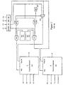
- FIG. 3 illustrates a CLB configuration including a synchronous, dual port RAM in accordance with the present invention.
- Figure 4 shows timing diagrams for the CLB illustrated in Figure 3.
- Figure 5 illustrates the write strobe logic in one embodiment of the present invention.
- Figures 6A and 6B show an address decoder, a multiplexer, and a function generator which illustrates the dual port capability of the present invention and one embodiment of a latch.
- Figure 3 illustrates a portion of a configurable logic block (CLB) which includes a function generator 301 having a dual port RAM.
- address decoder 305A provides signals to the Read Address terminals of function generator 301 as well as to multiplexer 306A.
- address decoder 305B provides signals to the Read Address terminals of function generator 302 as well as to multiplexer 306A.
- Multiplexer 306A provides output signals to the D input terminals of latch 304A which, in its transparent state (typically invoked upon receiving a logic one latch enable (LE) signal), provides those signals to the Write Address terminals of function generator 301.
- LE logic one latch enable
- FIGS 6A and 6B illustrates multiplexer 306A, address decoder 305A, latch 304A, and function generator 301 in greater detail.
- latch 304A is formed using pass transistors which temporarily store the signals in the gate capacitance of inverters 312 (provided a low latch enable signal LE is asserted).
- latch 304A is implemented as a static latch.
- Function generator 301 is configured such that during a write operation, the Q terminals of the memory cells are accessed. However, during a standard read operation the signals stored on the Q terminals of the memory cells are accessed. Therefore, inverters 313 are provided to ensure a Q output signal.
- the dual port mode is enabled by memory cell 308 providing a logic one control signal to multiplexer 306A, thereby transferring the address signals of address decoder 305B rather than the address signals of address decoder 305A to latch 304A.
- latch enable signal LE is high, thereby ensuring latches 304 are in their transparent state.
- the write location in function generator 301 is decoded from input signals F1-F4, and the read location is decoded from input signals G1-G4.
- Function generator 301 therefore has independent and asynchronous read and write addresses. In this manner, the user has the ability to simultaneously read a predetermined RAM cell designated by the input signals G1-G4 as well as the ability to write to a second predetermined RAM cell designated by the input signals F1-F4.
- memory cell 308 stores a logic one in the dual port mode, a logic zero signal is then provided to one of the input terminals of AND gate 307, thereby ensuring a logic zero output signal from this gate.
- This logic zero output signal activates multiplexer 306B to transfer the data signal DIN to a latch 304B which upon receiving a high latch enable signal LE (i.e. activating its transparent state) transfers the data signal DIN to the Data input terminal of function generator 301.
- the data signal DIN is also provided to a latch 304D, which upon being enabled by the same latch enable signal LE as latch 304B, transfers the data signal DIN to the Data input terminal of function generator 302. Therefore, in the dual port mode, data signal DIN is written to both function generator 301 and function generator 302.
- memory cell 308 stores a logic zero signal. That signal, provided to the control terminal of multiplexer 306A, transfers the address specified by input signals G1-G4 to latch 304A, which in its transparent state, is then provided to the Write Address terminals of function generator 301. Note that in this mode a logic one signal is provided to AND gate 307. Thus, the data signals provided to function generator 301 depend on the signal stored by memory cell 309. Specifically, if the signal stored by memory cell 309 is a logic one, then AND gate 307 outputs a logic one control signal to multiplexer 306B. This logic one signal activates multiplexer 306B to transfer data signal H1 to latch 304B. Once again, this signal is provided to the Data terminal of function generator 301 upon receiving a high latch enable signal LE.
- memory cell 309 determines whether the RAM cells of function generators 301 and 302 are formed in two 16x1 arrays or a single 32x1 array.
- a write operation is completed within one full period of a system clock.
- a selected edge of system clock signal 401 is used to lock the address and data input signals 402 and 403, and to generate a write strobe signal 406.
- Address and data signals 402 and 403 are latched for the duration of the active write strobe signal 406.
- the write strobe signal of the present invention is self-timed, thereby eliminating prior art timing considerations regarding the length of the active write enable signal WE 404, the stability of address and data signals 402 and 403 during an active write enable signal 404, and the hold time requirements.
- the write strobe signal is self-timed such that the width of this signal is sufficient to finish the memory cell write operation. After the memory cell write operation is finished, the write strobe signal is reset. Another write cycle may be initiated by the next system clock edge (selected by the user as explained in reference to Figure 5).
- FIG. 5 illustrates one embodiment of write strobe logic 500 which provides synchronous functionality.
- Circuit 501 determines whether the write operation is triggered by a rising or falling clock signal edge.
- a rising edge is chosen (also previously shown in Figure 4) by storing a logic zero signal in memory cell 501A. This logic zero signal turns off transistor 541, but because it is inverted by inverter 540 turns on transistor 542.
- a clock signal CLK is passed via inverter 543 and transistor 542, not via transistor 541.
- a rising clock edge on signal CLK is inverted by inverters 543 and 544, and then provided to NAND gate 503.
- the output signal of NAND gate 503, the latch enable signal LE is determined by the other input signals to NAND gate 503.
- signal DONE is high. This high signal is then inverted by inverter 538. In this manner, a low DONE signal is provided to NAND gate 503, thereby preventing the latch enable signal LE from going low during RAM initialization. Note that this low DONE signal is also provided to NAND gate 533, thereby forcing a high output signal RESET. In this manner, flip-flop 505 is initialized to its reset state (i.e. with a zero on its Q output terminal).
- the remaining input signal to NAND gate 503 is a signal provided by memory cell 502.
- memory cell 502 stores a logic low signal. This logic low signal ensures that NAND gate 503 outputs a high latch enable signal LE, thereby forcing latches 304A-304D ( Figure 3) to their transparent state.
- the memory cells of function generators 301 and 302 are then configured as standard RAM (i.e. without the synchronous feature).
- memory cell 502 stores a high signal.
- NAND gate 503 receives a high signal from memory cell 502 and a high DONE signal.
- circuit 501 After a rising clock edge, circuit 501 outputs a logic one signal. Therefore, NAND gate 503 generates a low output signal.
- This low latch enable signal LE ensures that latches 304 remain "closed", i.e. the output signals of latches 304A-304D retain their previous values irrespective of the D input signals, as long as the latch enable signal LE is low.
- This latching is shown by latched address signal 402A, latched data signal 403A, and latched write enable signal 404A in the high portion of the cycle of system clock 401 ( Figure 4).
- D flip-flop 504 receives the output signal of circuit 501 as a clock signal.
- the D input terminal of flip-flop 504 receives a write enable signal WE.
- the Q output terminal of flip-flop 504 is designated as node 505.
- the operation of flip-flop 504, which includes two conventional latches, is well known in the art, and therefore is not explained in detail herein.
- Transistors 506 and 507 form a 2x1 multiplexer 508 which transfers either the write enable signal WE or the signal on node 505. Because memory cell 502 provides a logic one in the synchronous RAM enabled mode, transistor 506 is turned on, whereas transistor 507 is turned off, thereby providing the signal on node 505 to inverter 509. The state of the signal on node 505 is determined by the state of flip-flop 504. Specifically, at this time, flip-flop 504 is in a reset state (i.e. NOR gate 545 receives a logic one signal from NAND gate 533) which was forced by the high DONE signal during RAM initialization. Therefore, node 505 has a logic zero signal. This low signal, transferred by conducting transistor 506, is inverted by inverter 509 and then provided to NOR gates 510 and 511, thereby ensuring that those gates inhibit write strobe signals WSG and WSF, respectively.
- NOR gate 545 receives a logic one signal from NAND gate 533
- write strobe signals WSG and WSF are low. These low signals initialize dummy memory cells 523, 524, 550, and 551 (described in detail below). Note that the operation of cell timing circuits 521 and 522 are identical, and therefore only cell timing circuit 521 is explained for illustration.
- the low write strobe signal WSG is inverted by inverter 527, thereby turning on transistors 525A and 525B.
- the high signal transferred by transistor 525A and the low signal transferred by transistor 525B are provided to the Q terminals of dummy memory cells 523 and 524, respectively.
- dummy memory cells 523 and 524 are initialized such that the Q terminals carry a logic zero signal and a logic one signal, respectively.
- Inverter 529 inverts the logic zero signal.
- NOR gate 530 receives a logic one signal from inverter 529 and a logic one signal from dummy memory cell 524, and outputs a logic zero signal to NOR gate 531. Therefore, the output signal of NOR gate 531 depends on its other input signals.
- write strobe signal 406 is asserted. Specifically, the generation of this strobe signal is enabled by the rising edge of system clock signal 401 in conjunction with a high state on the latched write enable signal 404A.
- a high clock signal CLK generates a low latch enable signal LE and at the same time triggers flip-flop 504.
- the logic one write enable signal WE provided to the D input terminal of flip-flop 504 is transferred to its Q output terminal (i.e. to node 505).
- the logic one output signal of multiplexer 508 is inverted by inverter 509 and then provided to NOR gates 510 and 511.
- the states of write strobe signals WSG and WSF are determined by the other signals provided to NOR gates 510 and 511. More specifically, the state of write strobe signal WSG is determined by memory cell 519, the DONE signal, the 16x2 signal, and the input signal H1. Similarly, the state of write strobe signal WSF is determined by memory cell 520, the DONE signal, the 16x2 signal, and the input signal H1 .
- Memory cells 519 and 520 determine whether function generators 301 and 302 are used as user writable RAM, respectively.
- logic zero signals stored in memory cells 519 and 520 disable the user RAM capability of function generators 301 and 302.
- a logic zero signal in memory cell 519 ensures that NAND gate 517 provides a logic one signal to NOR gate 510. That logic one signal, in turn, ensures that NOR gate 510 outputs a low (disabling) write strobe signal WSG.
- a logic zero signal in memory cell 520 ensures that NAND gate 518 provides a logic one signal to NOR gate 511. That logic one signal, in turn, ensures that NOR gate 511 outputs a low (disabling) write strobe signal WSF.
- NAND gates 517 and 518 both receive two logic one signals (recall the DONE signal is a logic one signal after RAM initialization). Therefore, NAND gates 517 and 518 output logic zero signals to NOR gates 510 and 511, respectively. Thus, the write strobe signals WSG and WSF are then dependent on the signals provided by NOR gates 512 and 513, respectively. If the 16x2 signal is low, thereby indicating that data signal DIN is written to one of the function generators, then input signal H1 determines which write strobe signal WSG or WSF goes high.
- both write strobe signals WSG and WSF go high.
- the 16x2 signal is assumed to be high.
- both strobe signals WSG and WSF go high, thereby indicating that a write operation is in process.
- memory cells 519 and 520 store different logic signals.
- Circuits 521 and 522 provide cell timing during a write operation. Each circuit includes two dummy memory cells.
- circuit 521 includes dummy memory cells 523 and 524.
- the Q terminals of those memory cells are coupled to a plurality of transistors designed to emulate the write data paths of the memory cells in function generators 301 and 302.
- transistors 560-563 emulate the n-channel transistor of inverter 600 and illustrative transistors 601-603 ( Figure 6B), respectively. Note that to ensure appropriate timing margin, transistor 560 is sized smaller than the n-channel transistor of inverter 600.
- the p-channel transistor of circuit 526B is sized smaller than the p-channel transistor of inverter 600.
- the Q terminal of dummy memory cell 523 is provided either a logic one signal from transistor 525A or a logic zero signal from a plurality of transistors 526A.
- the Q terminal of dummy memory cell 524 is provided a logic zero signal from either transistor 525B or a logic one from a plurality of transistors 526B.
- write strobe signal WSG goes high, then transistors 525A and 525B (via inverter 527) are turned off, and the plurality of transistors 526A are turned on. In this manner, dummy memory cell 523 is written to provide a logic one signal on its Q terminal and dummy memory cell 524 is written to provide a logic zero on its Q terminal. In other words, during an active write enable strobe signal, dummy memory cells 523 and 524 are written to their respective opposite states. Therefore, NOR gate 530 receives logic zero signals from both inverter 529 and dummy memory cell 524, and outputs a logic one signal. This logic one signal indicates that both dummy memory cells 523 and 524 have been successfully written to.
- the time for the RAM cells in function generator 301 ( Figure 3) to be written to (either a logic one or a logic zero) is the same for dummy memory cells 523 and 524.
- NOR gate 530 outputs a logic one signal, the RAM cells in function generator 301 have also completed their write operation.
- NOR gate 553 also generates a logic one output signal.
- a logic one signal from NAND gates 530 and 553 ensures that NOR gates 531 and 534 both provide logic zero signals to OR gate 532. Therefore, OR gate 532 outputs a logic zero signal to NAND gate 533.
- the OR gate 532 is provided to ensure that the write operations associated with both function generators 301 and 302 are completed.
- the logic zero output signal of OR gate 532 forces NAND gate 533 to provide a logic one (active) RESET signal, thereby resetting flip-flop 504.
- a high RESET signal forces write enable signal WEB to go high.
- NOR gates 510 and 511 which receive that high WEB signal, then output low (disabling) write strobe signals WSG and WSF.
- NOR gate 512 provides a logic one signal to NOR gate 531 (thereby initiating a reset operation) only if the input signal H1 and the 16x2 signal are low.
- NOR gate 513 provides a logic one signal to NOR gate 534 only if the input signal H1 and the 16x2 signal are low.
- NAND gate 533 If only one function generator reset signal, i.e. reset signal RGB or reset signal RFB, is low, then OR gate 532 outputs a logic one. Thus, the output signal of NAND gate 533 depends from the state of the DONE signal. As mentioned previously, after RAM initialization, the DONE signal is a logic zero. Therefore, NAND gate 533 receives two logic one signals, thereby outputting a logic zero RESET signal (i.e. not resetting flip-flop 504).
- the data input for the synchronous RAM in various configurations are the same as the corresponding configurations in a Xilinx XC4000 RAM, and therefore are not explained in detail herein.
Landscapes
- Engineering & Computer Science (AREA)
- Physics & Mathematics (AREA)
- Mathematical Physics (AREA)
- Computer Hardware Design (AREA)
- Computing Systems (AREA)
- General Engineering & Computer Science (AREA)
- Microelectronics & Electronic Packaging (AREA)
- Static Random-Access Memory (AREA)
- Logic Circuits (AREA)
Claims (22)
- Configuration de bloc logique configurable comprenant :un premier générateur de fonctions (301) incluant un premier ensemble de cellules de mémoire (MC); etun circuit logique d'échantillonnage d'écriture (303) couplé audit générateur de fonctions (301), ledit circuit logique d'échantillonnage d'écriture (303) incluant une paire de cellules de mémoire fictives (523, 524) pour émuler la programmation dudit premier ensemble de cellules de mémoire (MC).
- Configuration de bloc logique configurable de la revendication 1, comprenant en outre :un deuxième générateur de fonctions (302) incluant un deuxième ensemble de cellules de mémoire (MC); et où leditcircuit logique d'échantillonnage d'écriture (303) est couplé audit premier générateur de fonctions (301) et audit deuxième générateur de fonctions (302).
- La configuration de bloc logique configurable des revendications 1 ou 2;
dans laquelle ledit premier générateur de fonctions (301) inclut en outre une pluralité de chemins de données d'écriture (600, 601, 602, 603) connectés à des cellules de mémoire (MC) respectives; et
dans laquelle ledit circuit logique d'échantillonnage d'écriture (303) inclut un ensemble de transistors (526A, 526B) pour émuler le retard de signal à travers au moins un desdits chemins de données d'écriture. - La configuration de bloc logique configurable de l'une quelconque des revendications précédentes, dans laquelle ledit circuit logique d'échantillonnage d'écriture (303) inclut un premier transistor à canal n (560) pour émuler un transistor à canal n dans un inverseur (600) couplé audit premier générateur de fonctions (301).
- La configuration de bloc logique configurable de l'une quelconque des revendications 1, 2 ou 3, dans laquelle ledit circuit logique d'échantillonnage d'écriture (303) inclut un premier transistor à canal p (526B) pour émuler un transistor à canal p dans un inverseur (600) couplé audit premier générateur de fonctions.
- La configuration de bloc logique configurable de l'une quelconque des revendications précédentes comprenant en outre une pluralité de verrous où chaque générateur de fonctions (301) inclut en outre des bornes d'adresse d'écriture et des bornes d'adresse de lecture couplées auxdits verrous.
- La configuration de bloc logique configurable de la revendication 6, dans laquelle ledit circuit logique d'échantillonnage d'écriture (303) fournit un signal d'autorisation de verrou à chacun desdits verrous.
- La configuration de bloc logique configurable de la revendication 6 ou 7, dans laquelle chacun desdits verrous inclut une pluralité d'inverseurs et une pluralité de transistors de multiplication de courant, où lesdits transistors de multiplication de courant stockent temporairement des signaux dans les capacitances de grille de ladite pluralité d'inverseurs.
- La configuration de bloc logique configurable de l'une quelconque des revendications précédentes, dans laquelle ledit circuit logique d'échantillonnage d'écriture (303) inclut une cellule de mémoire pour déterminer si le ou chaque générateur de fonctions (301) fonctionne en un mode synchrone.
- La configuration de bloc logique configurable de la revendication 9, dans laquelle ledit circuit logique d'échantillonnage d'écriture (303) inclut un moyen pour fournir un signal d'échantillonnage d'écriture audit premier générateur de fonctions (301), où ledit moyen pour fournir ledit signal d'échantillonnage d'écriture reçoit un signal à porte forcé par l'état stocké de ladite première cellule de mémoire (MC) et un signal FAIT.
- La configuration de bloc logique configurable de la revendication 10, dans laquelle ledit moyen pour fournir un signal d'échantillonnage d'écriture reçoit en outre un signal tamponné de ladite bascule ou reçoit un signal tamponné d'autorisation à l'écriture.
- La configuration de bloc logique configurable selon la revendication 2 ou l'une quelconque des revendications 3 à 11 lorsqu'annexées à la revendication 2, dans laquelle ledit circuit logique d'échantillonnage d'écriture comprend une circuiterie d'adressage couplée auxdites bornes d'adresses de lecture et d'écriture desdits premier et deuxième générateurs de fonctions (301, 302), où un signal de commande fourni à ladite circuiterie d'adressage fournit un signal auxdites bornes d'adresse d'écriture desdits premier et deuxième générateurs de fonctions (301, 302).
- La configuration de bloc logique configurable de la revendication 12, dans laquelle ladite circuiterie d'adressage inclut un multiplexeur qui fournit sélectivement ledit signal.
- La configuration de bloc logique configurable de la revendication 13, dans laquelle ladite circuiterie d'adressage inclut en outre un verrou couplé entre ledit multiplexeur et la borne d'adresse d'écriture du ou de chaque générateur de fonctions (301, 302).
- La configuration de bloc logique configurable de la revendication 13, dans laquelle ladite circuiterie d'adressage inclut un décodeur d'adresses pour fournir un premier signal d'entrée audit multiplexeur et à ladite borne de lecture d'adresse de chacun desdits générateurs de fonctions (301, 302).
- La configuration de bloc logique configurable selon l'une quelconque des revendications précédentes, dans laquelle chaque générateur de fonctions (301, 302) comprend des cellules de mémoire à accès sélectif.
- La configuration de bloc logique configurable de la revendication 1, dans laquelle une première de ladite paire de cellules de mémoire fictives (523, 524) émule l'écriture d'un un logique dans une cellule de mémoire dans ledit premier ensemble de cellules de mémoire (MC), et où une deuxième de ladite paire de cellules de mémoire fictives (523, 524) émule l'écriture d'un zéro logique dans ladite cellule de mémoire dans ledit premier ensemble de cellules de mémoire.
- La configuration de bloc logique configurable de l'une quelconque des revendications précédentes, ledit circuit logique d'échantillonnage d'écriture incluant en outre :où l'une de ladite paire de cellules de mémoire fictives (523, 524) a une borne d'écriture (QB), commandée par ladite borne de sortie dudit circuit bistable et une borne de sortie (Q) de cellule de mémoire connectée à ladite borne de retour d'information dudit circuit bistable.un circuit bistable (504) ayant une borne d'autorisation à l'écriture (WE), une borne de retour d'information (RESET), et une borne de sortie (WEB); et
- Configuration de bloc logique configurable de la revendication 18, dans laquelle ledit circuit bistable est une bascule.
- La configuration de bloc logique configurable de la revendication 19, dans laquelle ladite borne de retour d'information dudit circuit bistable est une entrée de remise à zéro asynchrone de ladite bascule.
- La configuration de bloc logique configurable de la revendication 18, dans laquelle ladite deuxième cellule de mémoire fictive (524) est connectée en parallèle à ladite première cellule de mémoire fictive (523).
- La configuration de bloc logique configurable de la revendication 21, dans laquelle ladite cellule de mémoire fictive mentionnée en premier (523) est adaptée pour écrire un zéro logique en réponse à un signal d'autorisation à l'écriture sur ladite borne d'autorisation à l'écriture et où ladite deuxième cellule de mémoire fictive (524) est adaptée pour écrire un un logique en réponse audit signal d'autorisation à l'écriture sur ladite borne d'autorisation à l'écriture.
Priority Applications (1)
| Application Number | Priority Date | Filing Date | Title |
|---|---|---|---|
| EP01120245.4A EP1154435B1 (fr) | 1995-02-10 | 1996-02-09 | Circuit d'écriture pour mémoires RAM synchrones |
Applications Claiming Priority (2)
| Application Number | Priority Date | Filing Date | Title |
|---|---|---|---|
| US08/386,972 US5566123A (en) | 1995-02-10 | 1995-02-10 | Synchronous dual port ram |
| US386972 | 1995-02-10 |
Related Child Applications (1)
| Application Number | Title | Priority Date | Filing Date |
|---|---|---|---|
| EP01120245.4A Division EP1154435B1 (fr) | 1995-02-10 | 1996-02-09 | Circuit d'écriture pour mémoires RAM synchrones |
Publications (3)
| Publication Number | Publication Date |
|---|---|
| EP0726577A2 EP0726577A2 (fr) | 1996-08-14 |
| EP0726577A3 EP0726577A3 (fr) | 1998-11-25 |
| EP0726577B1 true EP0726577B1 (fr) | 2002-05-02 |
Family
ID=23527868
Family Applications (2)
| Application Number | Title | Priority Date | Filing Date |
|---|---|---|---|
| EP01120245.4A Expired - Lifetime EP1154435B1 (fr) | 1995-02-10 | 1996-02-09 | Circuit d'écriture pour mémoires RAM synchrones |
| EP96300872A Expired - Lifetime EP0726577B1 (fr) | 1995-02-10 | 1996-02-09 | Circuit d'écriture pour mémoire RAM synchrone |
Family Applications Before (1)
| Application Number | Title | Priority Date | Filing Date |
|---|---|---|---|
| EP01120245.4A Expired - Lifetime EP1154435B1 (fr) | 1995-02-10 | 1996-02-09 | Circuit d'écriture pour mémoires RAM synchrones |
Country Status (4)
| Country | Link |
|---|---|
| US (2) | US5566123A (fr) |
| EP (2) | EP1154435B1 (fr) |
| JP (1) | JP3868531B2 (fr) |
| DE (1) | DE69620934T2 (fr) |
Families Citing this family (94)
| Publication number | Priority date | Publication date | Assignee | Title |
|---|---|---|---|---|
| US5550782A (en) * | 1991-09-03 | 1996-08-27 | Altera Corporation | Programmable logic array integrated circuits |
| US6049223A (en) | 1995-03-22 | 2000-04-11 | Altera Corporation | Programmable logic array integrated circuit with general-purpose memory configurable as a random access or FIFO memory |
| US5757207A (en) | 1995-03-22 | 1998-05-26 | Altera Corporation | Programmable logic array integrated circuit incorporating a first-in first-out memory |
| US5804986A (en) * | 1995-12-29 | 1998-09-08 | Cypress Semiconductor Corp. | Memory in a programmable logic device |
| US5854918A (en) * | 1996-01-24 | 1998-12-29 | Ricoh Company Ltd. | Apparatus and method for self-timed algorithmic execution |
| US5623217A (en) * | 1996-02-26 | 1997-04-22 | Lucent Technologies Inc. | Field programmable gate array with write-port enabled memory |
| US5977791A (en) | 1996-04-15 | 1999-11-02 | Altera Corporation | Embedded memory block with FIFO mode for programmable logic device |
| US5715197A (en) | 1996-07-29 | 1998-02-03 | Xilinx, Inc. | Multiport RAM with programmable data port configuration |
| US5821776A (en) * | 1997-01-31 | 1998-10-13 | Actel Corporation | Field programmable gate array with mask programmed analog function circuits |
| US5959466A (en) | 1997-01-31 | 1999-09-28 | Actel Corporation | Field programmable gate array with mask programmed input and output buffers |
| US5909049A (en) | 1997-02-11 | 1999-06-01 | Actel Corporation | Antifuse programmed PROM cell |
| US5933369A (en) * | 1997-02-28 | 1999-08-03 | Xilinx, Inc. | RAM with synchronous write port using dynamic latches |
| US6150837A (en) | 1997-02-28 | 2000-11-21 | Actel Corporation | Enhanced field programmable gate array |
| US6249143B1 (en) | 1997-05-23 | 2001-06-19 | Altera Corporation | Programmable logic array integrated circuit with distributed random access memory array |
| US6020760A (en) * | 1997-07-16 | 2000-02-01 | Altera Corporation | I/O buffer circuit with pin multiplexing |
| US6011744A (en) * | 1997-07-16 | 2000-01-04 | Altera Corporation | Programmable logic device with multi-port memory |
| US6034857A (en) * | 1997-07-16 | 2000-03-07 | Altera Corporation | Input/output buffer with overcurrent protection circuit |
| US6078735A (en) * | 1997-09-29 | 2000-06-20 | Xilinx, Inc. | System and method for generating memory initialization logic in a target device with memory initialization bits from a programmable logic device |
| US6052327A (en) | 1997-10-14 | 2000-04-18 | Altera Corporation | Dual-port programmable logic device variable depth and width memory array |
| US6191998B1 (en) | 1997-10-16 | 2001-02-20 | Altera Corporation | Programmable logic device memory array circuit having combinable single-port memory arrays |
| US6288970B1 (en) | 1997-10-16 | 2001-09-11 | Altera Corporation | Programmable logic device memory array circuit having combinable single-port memory arrays |
| US6314499B1 (en) * | 1997-11-14 | 2001-11-06 | Lucent Technologies Inc. | Non-preemptive memory locking mechanism in a shared resource system |
| US6127843A (en) * | 1997-12-22 | 2000-10-03 | Vantis Corporation | Dual port SRAM memory for run time use in FPGA integrated circuits |
| US6031396A (en) * | 1998-06-12 | 2000-02-29 | National Semiconductor Corporation | Circuit for synchronizing asynchronous inputs using dual edge logic design |
| US6467017B1 (en) | 1998-06-23 | 2002-10-15 | Altera Corporation | Programmable logic device having embedded dual-port random access memory configurable as single-port memory |
| US6262933B1 (en) | 1999-01-29 | 2001-07-17 | Altera Corporation | High speed programmable address decoder |
| JP3270411B2 (ja) * | 1999-02-19 | 2002-04-02 | エヌイーシーマイクロシステム株式会社 | アドレス復号化装置 |
| US6486702B1 (en) | 1999-07-02 | 2002-11-26 | Altera Corporation | Embedded memory blocks for programmable logic |
| US6460061B1 (en) | 1999-10-29 | 2002-10-01 | Xilinx Inc. | 2-dimensional discrete cosine transform using a polynomial transform |
| US6388464B1 (en) * | 1999-12-30 | 2002-05-14 | Cypress Semiconductor Corp. | Configurable memory for programmable logic circuits |
| US6756811B2 (en) | 2000-03-10 | 2004-06-29 | Easic Corporation | Customizable and programmable cell array |
| US6331790B1 (en) | 2000-03-10 | 2001-12-18 | Easic Corporation | Customizable and programmable cell array |
| US6400635B1 (en) | 2000-03-15 | 2002-06-04 | Altera Corporation | Memory circuitry for programmable logic integrated circuit devices |
| US6356110B1 (en) | 2000-04-03 | 2002-03-12 | Altera Corporation San Jose Ca | Multifunction memory array in a programmable logic device |
| US6857043B1 (en) * | 2000-04-28 | 2005-02-15 | Altera Corporation | Shift register implementations of first-in/first-out memories utilizing a double increment gray code counter |
| US6462577B1 (en) | 2000-04-28 | 2002-10-08 | Altera Corporation | Configurable memory structures in a programmable logic device |
| US6411124B2 (en) | 2000-04-28 | 2002-06-25 | Altera Corporation | Programmable logic device logic modules with shift register capabilities |
| US6373279B1 (en) * | 2000-05-05 | 2002-04-16 | Xilinx, Inc. | FPGA lookup table with dual ended writes for ram and shift register modes |
| US6937063B1 (en) | 2000-09-02 | 2005-08-30 | Actel Corporation | Method and apparatus of memory clearing with monitoring RAM memory cells in a field programmable gated array |
| US6476636B1 (en) * | 2000-09-02 | 2002-11-05 | Actel Corporation | Tileable field-programmable gate array architecture |
| US6724220B1 (en) | 2000-10-26 | 2004-04-20 | Cyress Semiconductor Corporation | Programmable microcontroller architecture (mixed analog/digital) |
| US8103496B1 (en) | 2000-10-26 | 2012-01-24 | Cypress Semicondutor Corporation | Breakpoint control in an in-circuit emulation system |
| US7765095B1 (en) | 2000-10-26 | 2010-07-27 | Cypress Semiconductor Corporation | Conditional branching in an in-circuit emulation system |
| US8160864B1 (en) | 2000-10-26 | 2012-04-17 | Cypress Semiconductor Corporation | In-circuit emulator and pod synchronized boot |
| US8149048B1 (en) | 2000-10-26 | 2012-04-03 | Cypress Semiconductor Corporation | Apparatus and method for programmable power management in a programmable analog circuit block |
| US8176296B2 (en) | 2000-10-26 | 2012-05-08 | Cypress Semiconductor Corporation | Programmable microcontroller architecture |
| US6720796B1 (en) | 2001-05-06 | 2004-04-13 | Altera Corporation | Multiple size memories in a programmable logic device |
| EP1271783B1 (fr) * | 2001-06-29 | 2013-07-31 | Sicronic Remote KG, LLC | FPGA avec une interface simplifiée entre la mémoire de programme et les blocs logiques programmables |
| KR100416796B1 (ko) * | 2001-07-20 | 2004-01-31 | 삼성전자주식회사 | 반도체 메모리 장치의 명령어 디코더 및 디코딩 방법 |
| US7406674B1 (en) | 2001-10-24 | 2008-07-29 | Cypress Semiconductor Corporation | Method and apparatus for generating microcontroller configuration information |
| US8078970B1 (en) | 2001-11-09 | 2011-12-13 | Cypress Semiconductor Corporation | Graphical user interface with user-selectable list-box |
| US8042093B1 (en) | 2001-11-15 | 2011-10-18 | Cypress Semiconductor Corporation | System providing automatic source code generation for personalization and parameterization of user modules |
| US7844437B1 (en) | 2001-11-19 | 2010-11-30 | Cypress Semiconductor Corporation | System and method for performing next placements and pruning of disallowed placements for programming an integrated circuit |
| US8069405B1 (en) | 2001-11-19 | 2011-11-29 | Cypress Semiconductor Corporation | User interface for efficiently browsing an electronic document using data-driven tabs |
| US7774190B1 (en) | 2001-11-19 | 2010-08-10 | Cypress Semiconductor Corporation | Sleep and stall in an in-circuit emulation system |
| US6971004B1 (en) | 2001-11-19 | 2005-11-29 | Cypress Semiconductor Corp. | System and method of dynamically reconfiguring a programmable integrated circuit |
| US7770113B1 (en) | 2001-11-19 | 2010-08-03 | Cypress Semiconductor Corporation | System and method for dynamically generating a configuration datasheet |
| US6590826B1 (en) | 2002-01-22 | 2003-07-08 | Xilinx, Inc. | Self-addressing FIFO |
| US8103497B1 (en) | 2002-03-28 | 2012-01-24 | Cypress Semiconductor Corporation | External interface for event architecture |
| US7308608B1 (en) | 2002-05-01 | 2007-12-11 | Cypress Semiconductor Corporation | Reconfigurable testing system and method |
| EP1547089A2 (fr) * | 2002-08-29 | 2005-06-29 | Koninklijke Philips Electronics N.V. | Dispositif electronique reconfigurable comprenant des dispositifs de stockage de donnees interconnectes |
| US7761845B1 (en) | 2002-09-09 | 2010-07-20 | Cypress Semiconductor Corporation | Method for parameterizing a user module |
| US7111110B1 (en) | 2002-12-10 | 2006-09-19 | Altera Corporation | Versatile RAM for programmable logic device |
| US7796464B1 (en) | 2003-06-27 | 2010-09-14 | Cypress Semiconductor Corporation | Synchronous memory with a shadow-cycle counter |
| US7295049B1 (en) | 2004-03-25 | 2007-11-13 | Cypress Semiconductor Corporation | Method and circuit for rapid alignment of signals |
| US7562193B2 (en) * | 2004-04-19 | 2009-07-14 | Nokia Corporation | Memory with single and dual mode access |
| US7084665B1 (en) | 2004-07-22 | 2006-08-01 | Altera Corporation | Distributed random access memory in a programmable logic device |
| US7797701B1 (en) * | 2004-08-13 | 2010-09-14 | Xilinx, Inc. | Method and apparatus for detecting a bit sequence in a data stream |
| US8069436B2 (en) | 2004-08-13 | 2011-11-29 | Cypress Semiconductor Corporation | Providing hardware independence to automate code generation of processing device firmware |
| US7332976B1 (en) | 2005-02-04 | 2008-02-19 | Cypress Semiconductor Corporation | Poly-phase frequency synthesis oscillator |
| US7400183B1 (en) | 2005-05-05 | 2008-07-15 | Cypress Semiconductor Corporation | Voltage controlled oscillator delay cell and method |
| US8085067B1 (en) | 2005-12-21 | 2011-12-27 | Cypress Semiconductor Corporation | Differential-to-single ended signal converter circuit and method |
| US7391236B2 (en) * | 2005-12-27 | 2008-06-24 | Altera Corporation | Distributed memory in field-programmable gate array integrated circuit devices |
| US8067948B2 (en) | 2006-03-27 | 2011-11-29 | Cypress Semiconductor Corporation | Input/output multiplexer bus |
| US7668029B2 (en) | 2006-08-11 | 2010-02-23 | Freescale Semiconductor, Inc | Memory having sense time of variable duration |
| US9564902B2 (en) | 2007-04-17 | 2017-02-07 | Cypress Semiconductor Corporation | Dynamically configurable and re-configurable data path |
| US8040266B2 (en) | 2007-04-17 | 2011-10-18 | Cypress Semiconductor Corporation | Programmable sigma-delta analog-to-digital converter |
| US8516025B2 (en) | 2007-04-17 | 2013-08-20 | Cypress Semiconductor Corporation | Clock driven dynamic datapath chaining |
| US8092083B2 (en) | 2007-04-17 | 2012-01-10 | Cypress Semiconductor Corporation | Temperature sensor with digital bandgap |
| US8130025B2 (en) | 2007-04-17 | 2012-03-06 | Cypress Semiconductor Corporation | Numerical band gap |
| US8026739B2 (en) | 2007-04-17 | 2011-09-27 | Cypress Semiconductor Corporation | System level interconnect with programmable switching |
| US7737724B2 (en) | 2007-04-17 | 2010-06-15 | Cypress Semiconductor Corporation | Universal digital block interconnection and channel routing |
| US8065653B1 (en) | 2007-04-25 | 2011-11-22 | Cypress Semiconductor Corporation | Configuration of programmable IC design elements |
| US9720805B1 (en) | 2007-04-25 | 2017-08-01 | Cypress Semiconductor Corporation | System and method for controlling a target device |
| US8266575B1 (en) | 2007-04-25 | 2012-09-11 | Cypress Semiconductor Corporation | Systems and methods for dynamically reconfiguring a programmable system on a chip |
| US8049569B1 (en) | 2007-09-05 | 2011-11-01 | Cypress Semiconductor Corporation | Circuit and method for improving the accuracy of a crystal-less oscillator having dual-frequency modes |
| US8082401B2 (en) * | 2009-03-25 | 2011-12-20 | Qualcomm Incorporated | Self-timing for a multi-ported memory system |
| US9448964B2 (en) | 2009-05-04 | 2016-09-20 | Cypress Semiconductor Corporation | Autonomous control in a programmable system |
| US9507534B2 (en) | 2011-12-30 | 2016-11-29 | Intel Corporation | Home agent multi-level NVM memory architecture |
| US8913455B1 (en) | 2013-07-29 | 2014-12-16 | Xilinx, Inc. | Dual port memory cell |
| CN105022588B (zh) * | 2014-04-29 | 2018-06-22 | 晨星半导体股份有限公司 | 嵌入式装置、嵌入式装置的存储器硬盘以及存取嵌入式装置的存储器硬盘的方法 |
| US10049709B2 (en) * | 2015-12-31 | 2018-08-14 | Arm Limited | Port modes for use with memory |
| US10474390B1 (en) * | 2017-05-04 | 2019-11-12 | Xilinx, Inc. | Systems and method for buffering data using a delayed write data signal and a memory receiving write addresses in a first order and read addresses in a second order |
| KR102861563B1 (ko) * | 2020-07-09 | 2025-09-18 | 에스케이하이닉스 주식회사 | 메모리 장치 |
Family Cites Families (11)
| Publication number | Priority date | Publication date | Assignee | Title |
|---|---|---|---|---|
| US5027323A (en) * | 1988-01-14 | 1991-06-25 | Hitachi, Ltd. | Write pulse signal generating circuit for a semiconductor memory device |
| US4933909A (en) | 1988-12-19 | 1990-06-12 | Bull Hn Information Systems Inc. | Dual read/write register file memory |
| US5343406A (en) * | 1989-07-28 | 1994-08-30 | Xilinx, Inc. | Distributed memory architecture for a configurable logic array and method for using distributed memory |
| US5317209A (en) * | 1991-08-29 | 1994-05-31 | National Semiconductor Corporation | Dynamic three-state bussing capability in a configurable logic array |
| US5425036A (en) * | 1992-09-18 | 1995-06-13 | Quickturn Design Systems, Inc. | Method and apparatus for debugging reconfigurable emulation systems |
| JPH0757469A (ja) * | 1993-08-11 | 1995-03-03 | Nec Corp | メモリ回路 |
| US5315178A (en) * | 1993-08-27 | 1994-05-24 | Hewlett-Packard Company | IC which can be used as a programmable logic cell array or as a register file |
| US5349250A (en) * | 1993-09-02 | 1994-09-20 | Xilinx, Inc. | Logic structure and circuit for fast carry |
| US5448522A (en) * | 1994-03-24 | 1995-09-05 | Quickturn Design Systems, Inc. | Multi-port memory emulation using tag registers |
| US5513139A (en) * | 1994-11-04 | 1996-04-30 | General Instruments Corp. | Random access memory with circuitry for concurrently and sequentially writing-in and reading-out data at different rates |
| US5559450A (en) * | 1995-07-27 | 1996-09-24 | Lucent Technologies Inc. | Field programmable gate array with multi-port RAM |
-
1995
- 1995-02-10 US US08/386,972 patent/US5566123A/en not_active Expired - Lifetime
-
1996
- 1996-02-06 JP JP04425096A patent/JP3868531B2/ja not_active Expired - Lifetime
- 1996-02-09 DE DE69620934T patent/DE69620934T2/de not_active Expired - Lifetime
- 1996-02-09 EP EP01120245.4A patent/EP1154435B1/fr not_active Expired - Lifetime
- 1996-02-09 EP EP96300872A patent/EP0726577B1/fr not_active Expired - Lifetime
- 1996-06-21 US US08/668,276 patent/US5631577A/en not_active Expired - Lifetime
Also Published As
| Publication number | Publication date |
|---|---|
| DE69620934T2 (de) | 2002-11-21 |
| EP1154435B1 (fr) | 2015-08-26 |
| EP0726577A3 (fr) | 1998-11-25 |
| DE69620934D1 (de) | 2002-06-06 |
| EP1154435A2 (fr) | 2001-11-14 |
| EP1154435A3 (fr) | 2004-02-04 |
| EP0726577A2 (fr) | 1996-08-14 |
| US5631577A (en) | 1997-05-20 |
| JPH08263984A (ja) | 1996-10-11 |
| JP3868531B2 (ja) | 2007-01-17 |
| US5566123A (en) | 1996-10-15 |
Similar Documents
| Publication | Publication Date | Title |
|---|---|---|
| EP1154435B1 (fr) | Circuit d'écriture pour mémoires RAM synchrones | |
| US6353552B2 (en) | PLD with on-chip memory having a shadow register | |
| US5031146A (en) | Memory apparatus for multiple processor systems | |
| JP4521068B2 (ja) | パイプライン化デュアルポート集積回路メモリ | |
| JP3434822B2 (ja) | 構成可能な論理のダイナミック制御 | |
| US6298005B1 (en) | Configurable memory block | |
| US5867443A (en) | Shared bitline heterogeneous memory | |
| EP0554489A1 (fr) | Mémoire statique multiporte à accès aléatoire avec schème d'écriture à travers | |
| JPH0412554B2 (fr) | ||
| US4610004A (en) | Expandable four-port register file | |
| US5287485A (en) | Digital processing system including plural memory devices and data transfer circuitry | |
| US5193071A (en) | Memory apparatus for multiple processor systems | |
| US5933369A (en) | RAM with synchronous write port using dynamic latches | |
| US4241425A (en) | Organization for dynamic random access memory | |
| JPH10510087A (ja) | レジスタファイル読取/書込セル | |
| US5493530A (en) | Ram with pre-input register logic | |
| IL129310A (en) | Random access memory and process for writing to and reading from the same | |
| US6097651A (en) | Precharge circuitry in RAM circuit | |
| US5612923A (en) | Multi-port random access memory | |
| US6356487B1 (en) | Memory device having data path containing dual mode flip-flop used for normal operation and for internal testing | |
| JPH01137500A (ja) | 埋込み2進パターンを有するメモリ・アレイ装置 | |
| US5907508A (en) | Method and apparatus for single clocked, non-overlapping access in a multi-port memory cell | |
| EP0473819A1 (fr) | Cellule de mémoire multiporte | |
| KR100340067B1 (ko) | 데이터에 대한 읽기 및 쓰기 동작을 동시에 수행할 수있는 단일 포트 메모리 구조의 메모리 장치 | |
| US4766593A (en) | Monolithically integrated testable registers that cannot be directly addressed |
Legal Events
| Date | Code | Title | Description |
|---|---|---|---|
| PUAI | Public reference made under article 153(3) epc to a published international application that has entered the european phase |
Free format text: ORIGINAL CODE: 0009012 |
|
| AK | Designated contracting states |
Kind code of ref document: A2 Designated state(s): DE FR GB |
|
| PUAL | Search report despatched |
Free format text: ORIGINAL CODE: 0009013 |
|
| AK | Designated contracting states |
Kind code of ref document: A3 Designated state(s): DE FR GB |
|
| 17P | Request for examination filed |
Effective date: 19990422 |
|
| 17Q | First examination report despatched |
Effective date: 20000128 |
|
| GRAG | Despatch of communication of intention to grant |
Free format text: ORIGINAL CODE: EPIDOS AGRA |
|
| RTI1 | Title (correction) |
Free format text: WRITE CIRCUITRY FOR A SYNCHRONOUS RAM |
|
| GRAG | Despatch of communication of intention to grant |
Free format text: ORIGINAL CODE: EPIDOS AGRA |
|
| GRAG | Despatch of communication of intention to grant |
Free format text: ORIGINAL CODE: EPIDOS AGRA |
|
| GRAH | Despatch of communication of intention to grant a patent |
Free format text: ORIGINAL CODE: EPIDOS IGRA |
|
| GRAH | Despatch of communication of intention to grant a patent |
Free format text: ORIGINAL CODE: EPIDOS IGRA |
|
| REG | Reference to a national code |
Ref country code: GB Ref legal event code: IF02 |
|
| GRAA | (expected) grant |
Free format text: ORIGINAL CODE: 0009210 |
|
| AK | Designated contracting states |
Kind code of ref document: B1 Designated state(s): DE FR GB |
|
| REG | Reference to a national code |
Ref country code: GB Ref legal event code: FG4D |
|
| REF | Corresponds to: |
Ref document number: 69620934 Country of ref document: DE Date of ref document: 20020606 |
|
| ET | Fr: translation filed | ||
| PLBE | No opposition filed within time limit |
Free format text: ORIGINAL CODE: 0009261 |
|
| STAA | Information on the status of an ep patent application or granted ep patent |
Free format text: STATUS: NO OPPOSITION FILED WITHIN TIME LIMIT |
|
| 26N | No opposition filed |
Effective date: 20030204 |
|
| REG | Reference to a national code |
Ref country code: DE Ref legal event code: R082 Ref document number: 69620934 Country of ref document: DE Representative=s name: KOTITSCHKE & HEURUNG PARTNERSCHAFT MBB, DE Ref country code: DE Ref legal event code: R082 Ref document number: 69620934 Country of ref document: DE Representative=s name: KOTITSCHKE & HEURUNG PARTNERSCHAFT MBB PATENT-, DE |
|
| REG | Reference to a national code |
Ref country code: FR Ref legal event code: PLFP Year of fee payment: 20 |
|
| PGFP | Annual fee paid to national office [announced via postgrant information from national office to epo] |
Ref country code: DE Payment date: 20150226 Year of fee payment: 20 |
|
| PGFP | Annual fee paid to national office [announced via postgrant information from national office to epo] |
Ref country code: FR Payment date: 20150217 Year of fee payment: 20 Ref country code: GB Payment date: 20150226 Year of fee payment: 20 |
|
| REG | Reference to a national code |
Ref country code: DE Ref legal event code: R071 Ref document number: 69620934 Country of ref document: DE |
|
| REG | Reference to a national code |
Ref country code: GB Ref legal event code: PE20 Expiry date: 20160208 |
|
| PG25 | Lapsed in a contracting state [announced via postgrant information from national office to epo] |
Ref country code: GB Free format text: LAPSE BECAUSE OF EXPIRATION OF PROTECTION Effective date: 20160208 |