EP0726613A2 - Ebauche et procédé pour la fabrication d'ébauches et de produits semi-finis pour des contacts électriques - Google Patents
Ebauche et procédé pour la fabrication d'ébauches et de produits semi-finis pour des contacts électriques Download PDFInfo
- Publication number
- EP0726613A2 EP0726613A2 EP95114277A EP95114277A EP0726613A2 EP 0726613 A2 EP0726613 A2 EP 0726613A2 EP 95114277 A EP95114277 A EP 95114277A EP 95114277 A EP95114277 A EP 95114277A EP 0726613 A2 EP0726613 A2 EP 0726613A2
- Authority
- EP
- European Patent Office
- Prior art keywords
- strip
- coating
- contact carrier
- copper
- metal
- Prior art date
- Legal status (The legal status is an assumption and is not a legal conclusion. Google has not performed a legal analysis and makes no representation as to the accuracy of the status listed.)
- Granted
Links
Images
Classifications
-
- H—ELECTRICITY
- H01—ELECTRIC ELEMENTS
- H01R—ELECTRICALLY-CONDUCTIVE CONNECTIONS; STRUCTURAL ASSOCIATIONS OF A PLURALITY OF MUTUALLY-INSULATED ELECTRICAL CONNECTING ELEMENTS; COUPLING DEVICES; CURRENT COLLECTORS
- H01R43/00—Apparatus or processes specially adapted for manufacturing, assembling, maintaining, or repairing of line connectors or current collectors or for joining electric conductors
- H01R43/02—Apparatus or processes specially adapted for manufacturing, assembling, maintaining, or repairing of line connectors or current collectors or for joining electric conductors for soldered or welded connections
- H01R43/0214—Resistance welding
-
- H—ELECTRICITY
- H01—ELECTRIC ELEMENTS
- H01R—ELECTRICALLY-CONDUCTIVE CONNECTIONS; STRUCTURAL ASSOCIATIONS OF A PLURALITY OF MUTUALLY-INSULATED ELECTRICAL CONNECTING ELEMENTS; COUPLING DEVICES; CURRENT COLLECTORS
- H01R4/00—Electrically-conductive connections between two or more conductive members in direct contact, i.e. touching one another; Means for effecting or maintaining such contact; Electrically-conductive connections having two or more spaced connecting locations for conductors and using contact members penetrating insulation
- H01R4/02—Soldered or welded connections
- H01R4/029—Welded connections
Definitions
- the invention relates to a starting material for producing electrical contacts by connecting to an electrically conductive, essentially copper contact carrier tape by means of resistance heating, the preliminary material being designed as a metal tape with a contact area, which has a coating on its underside of the tape that can be connected to the contact carrier tape comprises a material which consists essentially of silver, the melting point of the material of the coating being below the melting point of the metal strip and a method for producing starting material and semi-finished product for electrical contacts.
- a starting material for the production of electrical contacts for example relay contacts
- the starting material is designed as a metal strip with a contact area, which by welding to an electrically conductive contact carrier also with an electrical conductivity of more than 15 m / (Ohm x mm 2 ) or more than (15 S x 10 6 ) / m is connected by means of resistance heating
- the contact carrier consists essentially of copper
- the strip surface side of the metal strip comprising the contact area has strand-like projections as weld nipples which contain a coating which essentially consists of silver, the melting point of the material of the coating being below the melting point of the metal strip
- the metal band is in essentially made of nickel, the actual contact area being formed on the basis of a gold alloy or silver-palladium alloy.
- the invention has for its object to provide a metal strip as a starting material for the production of electrical contacts, which has a contact profile of small profile width, and for resistance welding on a contact carrier tape high electrical conductivity of more than 15 m / (Ohm x mm 2 ) as they for example with copper, is suitable.
- the invention has for its object to provide a method for producing the metal strip as a raw material.
- a method for producing a semi-finished product for electrical contacts is to be specified, in which the metal strip is connected as a starting material to the contact carrier strip with high conductivity.
- the core area of the metal strip consists essentially of nickel; however, it is also possible to provide a core area made of a copper-nickel alloy.
- the contact area for the subsequent work contact preferably consists of a gold or a silver-palladium alloy; it can advantageously be applied together with the coating of the projections by roll cladding.
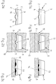
- FIG. 1a shows the metal strip 1 as the primary material, the auxiliary welding support or core area 2 essentially consisting of nickel or a copper-nickel-based alloy; an alloy with a nickel content of 30% by weight, an iron content of approximately 1% by weight and the rest copper are preferably used;
- the core area 2 of the metal strip consists of an alloy with a nickel content of 9% by weight, a tin content of 2% by weight and the rest copper.
- the actual contact area 3 for the subsequent work contact which essentially consists of noble metal, preferably of a gold alloy or silver-palladium alloy.
- the underside 4 of the core area 2 has a projection 5 as a weld nipple in its center, the entire underside 4 of the band being provided with a coating which essentially consists of silver.
- Both the core region 2 and the contact region 3 of the metal strip 1 have a trapezoidal outer circumference when viewed in cross section, the profile width increasing continuously in the direction of the projection 5.
- FIG. 1b shows the metal strip 1 placed on the contact carrier strip 8 in the electrode device; the coating 6 located on the strand-like projection 5 lies directly on the surface of the contact carrier strip 8.
- the welding circuit is closed via the electrodes 9 and 10, which are only partially shown, electrode 9 having a trapezoidal recess 11, seen in cross section, in which the metal strip is introduced with its top so that the metal strip 1 with its coated projection 5 is exact aligned on the surface 12 of the contact carrier tape 8 rests; the welding circuit is not shown here for a better overview. It can be seen from FIG.
- FIG. 1c shows in cross section a contact profile strand, after which it has left the electrode device partially shown in FIG. 1b and is firmly and mechanically connected to the contact carrier strip 8 underneath; 1c shows in a simple manner that the coating 6 originally located on the underside 4 of the metal strip has moved away from the projection 5 and the adjacent areas of the underside 4 and together with the copper in the area of the surface 12 of the contact carrier 8 Melting process formed by resistance heating connection area between contact carrier tape 8 and metal tape 1; During the actual welding process, the contact connection designated by number 13 according to FIG.
- Figure 2a shows a metal strip 1 'as a raw material, which is constructed essentially similar to that described with reference to Figure 1a;
- the band underside 4 ' has two strand-shaped grooves or depressions 16, 17, between which the strand-like projection 5 known from FIG. 1a is arranged.
- the depressions 16, 17 are geometrically designed such that they are filled by the volume of the melting lake 14 when they are welded onto the contact carrier strip 8 and thus prevent the alloy formed from swelling to the side.
- Nickel or a copper-nickel-based alloy is also preferably used as the material for the core region 2 or auxiliary welding support.
- the use of the metal strip 1 'in the electrode device is shown with reference to FIG. 2b, the metal strip 1' lying directly in the region of the projection 5 with the coating 6 on the surface 12 of the contact carrier strip 8.
- the two electrodes 9, 10 are only partially shown, the electrode device being omitted for a better overview.
- the trapezoidal recess 11 of the electrode 8 for the positive reception of the metal strip 1 ' can also be seen from FIG. 2b.
- FIG. 2c shows a cross-section of a contact profile strand after it has left the electrode device shown in FIG. 2b and the metal strip 1 'is firmly and mechanically connected to the contact carrier strip 8 by welding.
- the contact connection point designated by number 13 between the projection 5 with the silver coating 6 and the contact carrier 8 is heated so strongly by the action of the electric current that the silver emerges from the coating area of the projection and subsequently also from the strand-shaped depressions 16, 17 liquefies until the silver from the coating area and the copper from the contact carrier strip 8 alloy with one another and thus an alloy is formed which corresponds to the eutectic alloy with 28% by weight copper, the rest silver with a melting point at 779 ° C., or very obvious.
- the contact carrier tape is preferably made of copper, but it is also possible to use copper alloys such as bronze, nickel silver CuFe 2 or CuBe as the material for the contact carrier tape.
Landscapes
- Engineering & Computer Science (AREA)
- Manufacturing & Machinery (AREA)
- Contacts (AREA)
- Manufacture Of Switches (AREA)
- Electroplating Methods And Accessories (AREA)
Priority Applications (1)
| Application Number | Priority Date | Filing Date | Title |
|---|---|---|---|
| DE29522396U DE29522396U1 (de) | 1995-02-09 | 1995-09-12 | Vormaterial zur Herstellung elektrischer Kontakte |
Applications Claiming Priority (2)
| Application Number | Priority Date | Filing Date | Title |
|---|---|---|---|
| DE19504144A DE19504144C2 (de) | 1995-02-09 | 1995-02-09 | Vormaterial und Verfahren zur Herstellung von Vormaterial und Halbzeug für elektrische Kontakte |
| DE19504144 | 1995-02-09 |
Publications (3)
| Publication Number | Publication Date |
|---|---|
| EP0726613A2 true EP0726613A2 (fr) | 1996-08-14 |
| EP0726613A3 EP0726613A3 (fr) | 1997-09-10 |
| EP0726613B1 EP0726613B1 (fr) | 2000-03-01 |
Family
ID=7753464
Family Applications (1)
| Application Number | Title | Priority Date | Filing Date |
|---|---|---|---|
| EP95114277A Revoked EP0726613B1 (fr) | 1995-02-09 | 1995-09-12 | Ebauche et procédé pour la fabrication d'ébauches et de produits semi-finis pour des contacts électriques |
Country Status (3)
| Country | Link |
|---|---|
| US (1) | US5883352A (fr) |
| EP (1) | EP0726613B1 (fr) |
| DE (2) | DE19504144C2 (fr) |
Cited By (2)
| Publication number | Priority date | Publication date | Assignee | Title |
|---|---|---|---|---|
| DE19748288A1 (de) * | 1997-10-31 | 1999-05-06 | Kloeckner Moeller Gmbh | Schaltkontaktstück für Niederspannungs-Schaltgeräte |
| WO2020169295A1 (fr) * | 2019-02-20 | 2020-08-27 | Auto-Kabel Management Gmbh | Conducteur électrique ainsi que procédé de fabrication d'un conducteur électrique |
Families Citing this family (1)
| Publication number | Priority date | Publication date | Assignee | Title |
|---|---|---|---|---|
| EP1387370A1 (fr) * | 2002-08-03 | 2004-02-04 | INOVAN GmbH & Co. KG Metalle und Bauelemente | Demi-produit en forme de bande |
Family Cites Families (14)
| Publication number | Priority date | Publication date | Assignee | Title |
|---|---|---|---|---|
| US1155427A (en) * | 1914-11-20 | 1915-10-05 | Independent Lamp And Wire Company Inc | Contact bodies of tungsten. |
| US2181083A (en) * | 1936-01-02 | 1939-11-21 | Metals & Controls Corp | Laminated contact |
| US2281446A (en) * | 1937-01-07 | 1942-04-28 | Callite Tungsten Corp | Electrical contact |
| US2688574A (en) * | 1951-12-06 | 1954-09-07 | Western Electric Co | Method of making bimetal contact tape |
| US3191275A (en) * | 1961-09-26 | 1965-06-29 | Talon Inc | Method of making electrical contacts |
| US3346350A (en) * | 1965-05-25 | 1967-10-10 | Engelhard Ind Inc | Electrical contact tape |
| AU435640B2 (en) * | 1969-04-11 | 1973-05-14 | Chugai Electric Industrial Co. Ltd | A button type composite contact |
| JPS54133450A (en) * | 1978-04-10 | 1979-10-17 | Hitachi Ltd | Diffusion bonding method for different kind metal |
| DE2844888C2 (de) * | 1978-10-14 | 1983-02-24 | W.C. Heraeus Gmbh, 6450 Hanau | Vormaterial zur Herstellung elektrischer Kontakte |
| JPS607157A (ja) * | 1983-06-25 | 1985-01-14 | Masami Kobayashi | Ic用リ−ドフレ−ム |
| EP0301218B1 (fr) * | 1987-07-22 | 1991-11-21 | Siemens Aktiengesellschaft | Procédé de jonction de pièces au moyen de chauffage par résistance au moyen d'une impulsion d'énergie de courte durée |
| ATE94684T1 (de) * | 1987-07-22 | 1993-10-15 | Siemens Ag | Kontakt zum hartloeten auf einem traeger mittels widerstandspressschweissung mittels eines kurzzeit-energieimpulses. |
| JPH01151114A (ja) * | 1987-12-08 | 1989-06-13 | Tanaka Kikinzoku Kogyo Kk | 複合電気接点材料 |
| DE4216224C2 (de) * | 1992-05-19 | 1994-03-17 | Heraeus Gmbh W C | Vormaterial und Halbzeug für elektrische Kontakte sowie Verfahren zur Herstellung |
-
1995
- 1995-02-09 DE DE19504144A patent/DE19504144C2/de not_active Expired - Fee Related
- 1995-09-12 EP EP95114277A patent/EP0726613B1/fr not_active Revoked
- 1995-09-12 DE DE59507911T patent/DE59507911D1/de not_active Revoked
-
1996
- 1996-01-30 US US08/593,930 patent/US5883352A/en not_active Expired - Fee Related
Cited By (4)
| Publication number | Priority date | Publication date | Assignee | Title |
|---|---|---|---|---|
| DE19748288A1 (de) * | 1997-10-31 | 1999-05-06 | Kloeckner Moeller Gmbh | Schaltkontaktstück für Niederspannungs-Schaltgeräte |
| WO2020169295A1 (fr) * | 2019-02-20 | 2020-08-27 | Auto-Kabel Management Gmbh | Conducteur électrique ainsi que procédé de fabrication d'un conducteur électrique |
| US11394131B2 (en) | 2019-02-20 | 2022-07-19 | Auto-Kabel Management Gmbh | Electrical conductor and method for producing an electrical conductor |
| EP4239802A3 (fr) * | 2019-02-20 | 2023-11-08 | Auto-Kabel Management GmbH | Conducteur électrique et procédé de fabrication d'un conducteur électrique |
Also Published As
| Publication number | Publication date |
|---|---|
| DE59507911D1 (de) | 2000-04-06 |
| EP0726613A3 (fr) | 1997-09-10 |
| DE19504144A1 (de) | 1996-08-22 |
| US5883352A (en) | 1999-03-16 |
| DE19504144C2 (de) | 1998-09-24 |
| EP0726613B1 (fr) | 2000-03-01 |
Similar Documents
| Publication | Publication Date | Title |
|---|---|---|
| DE2844888C2 (de) | Vormaterial zur Herstellung elektrischer Kontakte | |
| DE69815356T2 (de) | Verfahren zum herstellen einer lötkolbenspitze und hergestellte lötkolbenspitze dafür | |
| DE69906220T2 (de) | Kohlenschleifstück | |
| DE10018276A1 (de) | Verbundscheibe | |
| DE1202854B (de) | Verfahren zur Herstellung einer gedruckten Schaltung | |
| DE102022207742A1 (de) | Spulenkomponente | |
| DE3237980C2 (de) | Verfahren zur Herstellung einer Kontaktanordnung | |
| EP1313109A2 (fr) | Résistance à montage en surface | |
| EP0726613B1 (fr) | Ebauche et procédé pour la fabrication d'ébauches et de produits semi-finis pour des contacts électriques | |
| DE2835022C2 (de) | Anodenkörper für einen Festelektrolytkondensator | |
| DE3785140T2 (de) | Verfahren zur herstellung einer verschweissten elektrischen kontaktanordnung. | |
| EP0570662B1 (fr) | Ebauche pour la production de contacts électriques, ainsi que fabrication et utilisation de l'ébauche | |
| DE2259792C3 (de) | Verfahren zur Herstellung eines elektrischen Mehrschichten-Kontaktstücks | |
| DE2747087A1 (de) | Zusammengesetztes material fuer elektrische kontakte | |
| DE3006275C2 (de) | Unterbrecherkontakt für Vakuumschalter | |
| DE3504861A1 (de) | Widerstandsverbindungsverfahren zum loeten oder schweissen metastabiler metalle | |
| DE3107665A1 (de) | "metallhalbzeug" | |
| EP0001750A1 (fr) | Procédé de fixation d'un conducteur de connexion sur une résistance électrique à coefficient de température positif | |
| DE1052580B (de) | Verfahren zum Herstellen einer elektrischen Entladungsroehre | |
| DE29522396U1 (de) | Vormaterial zur Herstellung elektrischer Kontakte | |
| DE3928960A1 (de) | Verfahren zum formen einer litze sowie derart geformte litze | |
| DE102008020582B4 (de) | Widerstandsschweissverfahren und Leitereinheit | |
| DE2530704C3 (de) | Verbundwerkstoff als Halbzeug für elektrische Kontaktstucke und Herstellungsverfahren hierzu | |
| DE69704025T2 (de) | Verfahren zur herstellung eines elektromechanischen relais | |
| DE1500715A1 (de) | Verfahren zum Verbinden zweier Metallteile |
Legal Events
| Date | Code | Title | Description |
|---|---|---|---|
| PUAI | Public reference made under article 153(3) epc to a published international application that has entered the european phase |
Free format text: ORIGINAL CODE: 0009012 |
|
| 17P | Request for examination filed |
Effective date: 19950927 |
|
| AK | Designated contracting states |
Kind code of ref document: A2 Designated state(s): DE FR GB IT |
|
| PUAL | Search report despatched |
Free format text: ORIGINAL CODE: 0009013 |
|
| AK | Designated contracting states |
Kind code of ref document: A3 Designated state(s): DE FR GB IT |
|
| 17Q | First examination report despatched |
Effective date: 19980824 |
|
| GRAG | Despatch of communication of intention to grant |
Free format text: ORIGINAL CODE: EPIDOS AGRA |
|
| RAP1 | Party data changed (applicant data changed or rights of an application transferred) |
Owner name: W.C. HERAEUS GMBH & CO. KG |
|
| GRAG | Despatch of communication of intention to grant |
Free format text: ORIGINAL CODE: EPIDOS AGRA |
|
| GRAG | Despatch of communication of intention to grant |
Free format text: ORIGINAL CODE: EPIDOS AGRA |
|
| GRAH | Despatch of communication of intention to grant a patent |
Free format text: ORIGINAL CODE: EPIDOS IGRA |
|
| GRAH | Despatch of communication of intention to grant a patent |
Free format text: ORIGINAL CODE: EPIDOS IGRA |
|
| GRAA | (expected) grant |
Free format text: ORIGINAL CODE: 0009210 |
|
| AK | Designated contracting states |
Kind code of ref document: B1 Designated state(s): DE FR GB IT |
|
| GBT | Gb: translation of ep patent filed (gb section 77(6)(a)/1977) |
Effective date: 20000301 |
|
| REF | Corresponds to: |
Ref document number: 59507911 Country of ref document: DE Date of ref document: 20000406 |
|
| ITF | It: translation for a ep patent filed | ||
| ET | Fr: translation filed | ||
| PLBQ | Unpublished change to opponent data |
Free format text: ORIGINAL CODE: EPIDOS OPPO |
|
| PLBI | Opposition filed |
Free format text: ORIGINAL CODE: 0009260 |
|
| PLBF | Reply of patent proprietor to notice(s) of opposition |
Free format text: ORIGINAL CODE: EPIDOS OBSO |
|
| 26 | Opposition filed |
Opponent name: AMI DODUCO GMBH Effective date: 20001124 |
|
| PLBF | Reply of patent proprietor to notice(s) of opposition |
Free format text: ORIGINAL CODE: EPIDOS OBSO |
|
| REG | Reference to a national code |
Ref country code: GB Ref legal event code: IF02 |
|
| PGFP | Annual fee paid to national office [announced via postgrant information from national office to epo] |
Ref country code: GB Payment date: 20020904 Year of fee payment: 8 |
|
| PGFP | Annual fee paid to national office [announced via postgrant information from national office to epo] |
Ref country code: DE Payment date: 20020907 Year of fee payment: 8 |
|
| PGFP | Annual fee paid to national office [announced via postgrant information from national office to epo] |
Ref country code: FR Payment date: 20020909 Year of fee payment: 8 |
|
| RDAH | Patent revoked |
Free format text: ORIGINAL CODE: EPIDOS REVO |
|
| RDAG | Patent revoked |
Free format text: ORIGINAL CODE: 0009271 |
|
| STAA | Information on the status of an ep patent application or granted ep patent |
Free format text: STATUS: PATENT REVOKED |
|
| 27W | Patent revoked |
Effective date: 20021124 |
|
| GBC | Gb: translation of claims filed (gb section 78(7)/1977) |
Free format text: 20021124 |
|
| PLAB | Opposition data, opponent's data or that of the opponent's representative modified |
Free format text: ORIGINAL CODE: 0009299OPPO |