EP0727670A2 - Circuit de mesure de différence de phase - Google Patents
Circuit de mesure de différence de phase Download PDFInfo
- Publication number
- EP0727670A2 EP0727670A2 EP96101354A EP96101354A EP0727670A2 EP 0727670 A2 EP0727670 A2 EP 0727670A2 EP 96101354 A EP96101354 A EP 96101354A EP 96101354 A EP96101354 A EP 96101354A EP 0727670 A2 EP0727670 A2 EP 0727670A2
- Authority
- EP
- European Patent Office
- Prior art keywords
- output
- input
- signal
- binary word
- shift register
- Prior art date
- Legal status (The legal status is an assumption and is not a legal conclusion. Google has not performed a legal analysis and makes no representation as to the accuracy of the status listed.)
- Granted
Links
Images

Classifications
-
- G—PHYSICS
- G01—MEASURING; TESTING
- G01R—MEASURING ELECTRIC VARIABLES; MEASURING MAGNETIC VARIABLES
- G01R25/00—Arrangements for measuring phase angle between a voltage and a current or between voltages or currents
-
- G—PHYSICS
- G01—MEASURING; TESTING
- G01R—MEASURING ELECTRIC VARIABLES; MEASURING MAGNETIC VARIABLES
- G01R31/00—Arrangements for testing electric properties; Arrangements for locating electric faults; Arrangements for electrical testing characterised by what is being tested not provided for elsewhere
- G01R31/28—Testing of electronic circuits, e.g. by signal tracer
- G01R31/317—Testing of digital circuits
- G01R31/3181—Functional testing
- G01R31/3185—Reconfiguring for testing, e.g. LSSD, partitioning
Definitions
- a counter 3 driven by the clock signal T pays continuously from zero to its maximum count, in order to then start again from zero. All binary words are run through from zero to the maximum value.
- the output of the counter 3 is fed to the input of a buffer 4 which, when the corresponding signal S1 occurs, takes over the binary word Z currently present at the output of the counter 3 and stores it until it is taken over again.
- the binary word located in the intermediate memory 4 is removable at the output of the intermediate memory 4 and forms the higher-order digits MSBs of an output binary word B indicating the phase difference between the reference signal R and the clock signal T.
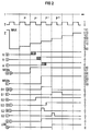
- FIG. 2 of the drawing the courses of the signals T, Z, MSBs, S1, S2, S3, LSB for three different phase positions of the reference signal R are shown over time t.
- the three cases are denoted by a, b and c in the drawing.
- the time grid is predetermined by the period P of the clock signal T.
- the master clock TM and the slave clock TS are derived from the clock signal, neither of which overlap on the edges.
Landscapes
- Physics & Mathematics (AREA)
- General Physics & Mathematics (AREA)
- Engineering & Computer Science (AREA)
- General Engineering & Computer Science (AREA)
- Measuring Phase Differences (AREA)
- Manipulation Of Pulses (AREA)
- Analogue/Digital Conversion (AREA)
Applications Claiming Priority (2)
| Application Number | Priority Date | Filing Date | Title |
|---|---|---|---|
| DE19506007 | 1995-02-17 | ||
| DE19506007A DE19506007C1 (de) | 1995-02-17 | 1995-02-17 | Schaltungsanordnung zur Phasendifferenzmessung |
Publications (3)
| Publication Number | Publication Date |
|---|---|
| EP0727670A2 true EP0727670A2 (fr) | 1996-08-21 |
| EP0727670A3 EP0727670A3 (fr) | 1997-06-18 |
| EP0727670B1 EP0727670B1 (fr) | 2006-11-22 |
Family
ID=7754655
Family Applications (1)
| Application Number | Title | Priority Date | Filing Date |
|---|---|---|---|
| EP96101354A Expired - Lifetime EP0727670B1 (fr) | 1995-02-17 | 1996-01-31 | Circuit de mesure de différence de phase |
Country Status (7)
| Country | Link |
|---|---|
| US (1) | US5903144A (fr) |
| EP (1) | EP0727670B1 (fr) |
| JP (1) | JPH08248071A (fr) |
| KR (1) | KR960032000A (fr) |
| CA (1) | CA2169616A1 (fr) |
| DE (2) | DE19506007C1 (fr) |
| TW (1) | TW282514B (fr) |
Families Citing this family (1)
| Publication number | Priority date | Publication date | Assignee | Title |
|---|---|---|---|---|
| US6388482B1 (en) | 2000-06-21 | 2002-05-14 | Infineon Technologies North America Corp. | DLL lock scheme with multiple phase detection |
Family Cites Families (5)
| Publication number | Priority date | Publication date | Assignee | Title |
|---|---|---|---|---|
| US4644268A (en) * | 1985-04-08 | 1987-02-17 | Allied-Signal Corporation | Apparatus and method for determining the magnitude and phase of the fundamental component of a complex waveshape |
| US4704574A (en) * | 1986-08-26 | 1987-11-03 | Rca Corporation | Phase difference measurement apparatus and method |
| US4926115A (en) * | 1988-12-19 | 1990-05-15 | Ag Communication Systems Corporation | Unique phase difference measuring circuit |
| DE59006912D1 (de) * | 1990-06-26 | 1994-09-29 | Siemens Ag | Verfahren zum Messen kleiner Phasendifferenzen und Schaltungsanordnung zur Durchführung des Verfahrens. |
| KR970000905B1 (ko) * | 1994-05-30 | 1997-01-21 | 대우전자 주식회사 | 위상차 측정 시스템 |
-
1995
- 1995-02-17 DE DE19506007A patent/DE19506007C1/de not_active Expired - Fee Related
- 1995-12-27 TW TW084113932A patent/TW282514B/zh active
-
1996
- 1996-01-31 DE DE59611400T patent/DE59611400D1/de not_active Expired - Fee Related
- 1996-01-31 EP EP96101354A patent/EP0727670B1/fr not_active Expired - Lifetime
- 1996-02-09 JP JP8047904A patent/JPH08248071A/ja not_active Withdrawn
- 1996-02-12 KR KR1019960003285A patent/KR960032000A/ko not_active Abandoned
- 1996-02-15 CA CA002169616A patent/CA2169616A1/fr not_active Abandoned
- 1996-02-20 US US08/603,930 patent/US5903144A/en not_active Expired - Fee Related
Also Published As
| Publication number | Publication date |
|---|---|
| KR960032000A (ko) | 1996-09-17 |
| EP0727670B1 (fr) | 2006-11-22 |
| JPH08248071A (ja) | 1996-09-27 |
| TW282514B (fr) | 1996-08-01 |
| DE19506007C1 (de) | 1996-02-22 |
| CA2169616A1 (fr) | 1996-08-18 |
| DE59611400D1 (de) | 2007-01-04 |
| EP0727670A3 (fr) | 1997-06-18 |
| US5903144A (en) | 1999-05-11 |
Similar Documents
| Publication | Publication Date | Title |
|---|---|---|
| DE2536585C3 (de) | Anordnung zur statistischen Signalanalyse | |
| DE3120669C2 (de) | A/D - und D/A - Umsetzer | |
| DE4304702A1 (en) | High speed serial to parallel converter for data transmission - has input data stream fed to pair of parallel multi stage registers with outputs generated via selector controlled by compressor | |
| DE2131635A1 (de) | Digitale Komprimierschaltung | |
| EP0099142A2 (fr) | Procédé et dispositif de démodulation d'un signal d'entrée modulé en fréquence | |
| DE2235802C2 (de) | Verfahren und Einrichtung zur Prüfung nichtlinearer Schaltkreise | |
| DE3533467C2 (de) | Verfahren und Anordnung zum störsicheren Erkennen von in Datensignalen enthaltenen Daten | |
| EP0727670B1 (fr) | Circuit de mesure de différence de phase | |
| EP0515438A1 (fr) | Procede de conversion d'une tension analogique en valeur numerique. | |
| DE69323545T2 (de) | Bit serieller dekodierer | |
| DE3046772C2 (de) | Taktgenerator | |
| DE19645057C2 (de) | Vorrichtung zur Selektion von Adressenwörtern mittels Demultiplex-Decodierung | |
| DE2426648C3 (de) | Schaltungsanordnung zur Erzeugung von Interpolations mpulsen | |
| DE1958662A1 (de) | Digitaler Impulsfolgenteiler mit optimaler Gleichverteilung der aus einer aequidistanten Eingangsimpulsfolge ausgewaehlten Impulse einer Ausgangsimpulsfolge | |
| DE1925917B2 (de) | Binaere impulsfrequenz-multiplizierschaltung | |
| DE3246211A1 (de) | Schaltungsanordnung zur detektion von folgen identischer binaerwerte | |
| DE2834751C2 (fr) | ||
| DE4236768C2 (de) | Frequenzteiler | |
| DE19513795C1 (de) | Schaltungsanordnung zur digitalen Phasendifferenzmessung | |
| DE1437669A1 (de) | System zum Umwandeln von Daten | |
| DE3432837A1 (de) | Datenkompressions- und datenexpandiereinrichtung zum uebertragen bzw. speichern von daten | |
| EP0283662B1 (fr) | Méthode et dispositif de traitement de données numériques asynchrones | |
| DE3720626C2 (fr) | ||
| DE1412097C (de) | Elektronisches Schrittschaltwerk in Form einer Ringschaltung | |
| DE1958662C (de) | Digitaler Impulsfolgenteiler mit optimaler Gleichverteilung der aus einer äquidistanten Eingangsimpulsfolge ausgewählten Impulse einer Ausgangsimpulsfolge |
Legal Events
| Date | Code | Title | Description |
|---|---|---|---|
| PUAI | Public reference made under article 153(3) epc to a published international application that has entered the european phase |
Free format text: ORIGINAL CODE: 0009012 |
|
| AK | Designated contracting states |
Kind code of ref document: A2 Designated state(s): CH DE FR GB IT LI SE |
|
| PUAL | Search report despatched |
Free format text: ORIGINAL CODE: 0009013 |
|
| AK | Designated contracting states |
Kind code of ref document: A3 Designated state(s): CH DE FR GB IT LI SE |
|
| 17P | Request for examination filed |
Effective date: 19970721 |
|
| RAP1 | Party data changed (applicant data changed or rights of an application transferred) |
Owner name: INFINEON TECHNOLOGIES AG |
|
| REG | Reference to a national code |
Ref country code: HK Ref legal event code: WD Ref document number: 1003725 Country of ref document: HK |
|
| GRAP | Despatch of communication of intention to grant a patent |
Free format text: ORIGINAL CODE: EPIDOSNIGR1 |
|
| GRAS | Grant fee paid |
Free format text: ORIGINAL CODE: EPIDOSNIGR3 |
|
| GRAA | (expected) grant |
Free format text: ORIGINAL CODE: 0009210 |
|
| AK | Designated contracting states |
Kind code of ref document: B1 Designated state(s): CH DE FR GB IT LI SE |
|
| PG25 | Lapsed in a contracting state [announced via postgrant information from national office to epo] |
Ref country code: IT Free format text: LAPSE BECAUSE OF FAILURE TO SUBMIT A TRANSLATION OF THE DESCRIPTION OR TO PAY THE FEE WITHIN THE PRE;WARNING: LAPSES OF ITALIAN PATENTS WITH EFFECTIVE DATE BEFORE 2007 MAY HAVE OCCURRED AT ANY TIME BEFORE 2007. THE CORRECT EFFECTIVE DATE MAY BE DIFFERENT FROM THE ONE RECORDED.SCRIBED TIME-LIMIT Effective date: 20061122 |
|
| REG | Reference to a national code |
Ref country code: GB Ref legal event code: FG4D Free format text: NOT ENGLISH |
|
| REG | Reference to a national code |
Ref country code: CH Ref legal event code: EP |
|
| REF | Corresponds to: |
Ref document number: 59611400 Country of ref document: DE Date of ref document: 20070104 Kind code of ref document: P |
|
| PG25 | Lapsed in a contracting state [announced via postgrant information from national office to epo] |
Ref country code: LI Free format text: LAPSE BECAUSE OF NON-PAYMENT OF DUE FEES Effective date: 20070131 Ref country code: CH Free format text: LAPSE BECAUSE OF NON-PAYMENT OF DUE FEES Effective date: 20070131 |
|
| PG25 | Lapsed in a contracting state [announced via postgrant information from national office to epo] |
Ref country code: SE Free format text: LAPSE BECAUSE OF FAILURE TO SUBMIT A TRANSLATION OF THE DESCRIPTION OR TO PAY THE FEE WITHIN THE PRESCRIBED TIME-LIMIT Effective date: 20070222 |
|
| GBV | Gb: ep patent (uk) treated as always having been void in accordance with gb section 77(7)/1977 [no translation filed] |
Effective date: 20061122 |
|
| EN | Fr: translation not filed | ||
| PG25 | Lapsed in a contracting state [announced via postgrant information from national office to epo] |
Ref country code: DE Free format text: LAPSE BECAUSE OF NON-PAYMENT OF DUE FEES Effective date: 20070801 |
|
| REG | Reference to a national code |
Ref country code: CH Ref legal event code: PL |
|
| PLBE | No opposition filed within time limit |
Free format text: ORIGINAL CODE: 0009261 |
|
| STAA | Information on the status of an ep patent application or granted ep patent |
Free format text: STATUS: NO OPPOSITION FILED WITHIN TIME LIMIT |
|
| 26N | No opposition filed |
Effective date: 20070823 |
|
| PG25 | Lapsed in a contracting state [announced via postgrant information from national office to epo] |
Ref country code: GB Free format text: LAPSE BECAUSE OF FAILURE TO SUBMIT A TRANSLATION OF THE DESCRIPTION OR TO PAY THE FEE WITHIN THE PRESCRIBED TIME-LIMIT Effective date: 20061122 |
|
| PG25 | Lapsed in a contracting state [announced via postgrant information from national office to epo] |
Ref country code: FR Free format text: LAPSE BECAUSE OF FAILURE TO SUBMIT A TRANSLATION OF THE DESCRIPTION OR TO PAY THE FEE WITHIN THE PRESCRIBED TIME-LIMIT Effective date: 20070713 |
|
| PG25 | Lapsed in a contracting state [announced via postgrant information from national office to epo] |
Ref country code: FR Free format text: LAPSE BECAUSE OF FAILURE TO SUBMIT A TRANSLATION OF THE DESCRIPTION OR TO PAY THE FEE WITHIN THE PRESCRIBED TIME-LIMIT Effective date: 20061122 |