EP0727832B1 - Procédé de fabrication d'une couche mince piézoélectrique - Google Patents
Procédé de fabrication d'une couche mince piézoélectrique Download PDFInfo
- Publication number
- EP0727832B1 EP0727832B1 EP19960102532 EP96102532A EP0727832B1 EP 0727832 B1 EP0727832 B1 EP 0727832B1 EP 19960102532 EP19960102532 EP 19960102532 EP 96102532 A EP96102532 A EP 96102532A EP 0727832 B1 EP0727832 B1 EP 0727832B1
- Authority
- EP
- European Patent Office
- Prior art keywords
- thin film
- piezoelectric
- annealing
- film
- gel
- Prior art date
- Legal status (The legal status is an assumption and is not a legal conclusion. Google has not performed a legal analysis and makes no representation as to the accuracy of the status listed.)
- Expired - Lifetime
Links
- 239000010409 thin film Substances 0.000 title claims description 256
- 238000000034 method Methods 0.000 title claims description 56
- 238000000137 annealing Methods 0.000 claims description 76
- 239000010408 film Substances 0.000 claims description 73
- 239000013078 crystal Substances 0.000 claims description 44
- 239000000758 substrate Substances 0.000 claims description 43
- 238000000576 coating method Methods 0.000 claims description 34
- 239000011248 coating agent Substances 0.000 claims description 31
- 239000000203 mixture Substances 0.000 claims description 30
- 229910052751 metal Inorganic materials 0.000 claims description 21
- 239000002184 metal Substances 0.000 claims description 21
- 238000005245 sintering Methods 0.000 claims description 20
- 229910044991 metal oxide Inorganic materials 0.000 claims description 19
- 150000004706 metal oxides Chemical class 0.000 claims description 19
- 238000003980 solgel method Methods 0.000 claims description 12
- 150000001875 compounds Chemical class 0.000 claims description 4
- 238000001035 drying Methods 0.000 claims description 3
- 239000005300 metallic glass Substances 0.000 claims description 2
- 229920000642 polymer Polymers 0.000 claims 1
- BASFCYQUMIYNBI-UHFFFAOYSA-N platinum Chemical compound [Pt] BASFCYQUMIYNBI-UHFFFAOYSA-N 0.000 description 22
- 238000004151 rapid thermal annealing Methods 0.000 description 15
- 238000003475 lamination Methods 0.000 description 13
- QTBSBXVTEAMEQO-UHFFFAOYSA-N Acetic acid Chemical compound CC(O)=O QTBSBXVTEAMEQO-UHFFFAOYSA-N 0.000 description 12
- QVGXLLKOCUKJST-UHFFFAOYSA-N atomic oxygen Chemical compound [O] QVGXLLKOCUKJST-UHFFFAOYSA-N 0.000 description 12
- 238000005336 cracking Methods 0.000 description 12
- 229910052760 oxygen Inorganic materials 0.000 description 12
- 239000001301 oxygen Substances 0.000 description 12
- 229910052697 platinum Inorganic materials 0.000 description 11
- 238000002441 X-ray diffraction Methods 0.000 description 10
- 230000015572 biosynthetic process Effects 0.000 description 10
- XUIMIQQOPSSXEZ-UHFFFAOYSA-N Silicon Chemical compound [Si] XUIMIQQOPSSXEZ-UHFFFAOYSA-N 0.000 description 9
- 229910052710 silicon Inorganic materials 0.000 description 9
- 239000010703 silicon Substances 0.000 description 9
- 229910052451 lead zirconate titanate Inorganic materials 0.000 description 8
- VXUYXOFXAQZZMF-UHFFFAOYSA-N titanium(IV) isopropoxide Chemical compound CC(C)O[Ti](OC(C)C)(OC(C)C)OC(C)C VXUYXOFXAQZZMF-UHFFFAOYSA-N 0.000 description 8
- 229910052782 aluminium Inorganic materials 0.000 description 7
- XAGFODPZIPBFFR-UHFFFAOYSA-N aluminium Chemical compound [Al] XAGFODPZIPBFFR-UHFFFAOYSA-N 0.000 description 7
- 238000005033 Fourier transform infrared spectroscopy Methods 0.000 description 6
- MTHSVFCYNBDYFN-UHFFFAOYSA-N diethylene glycol Chemical compound OCCOCCO MTHSVFCYNBDYFN-UHFFFAOYSA-N 0.000 description 6
- 238000004519 manufacturing process Methods 0.000 description 6
- 238000004544 sputter deposition Methods 0.000 description 6
- 238000010438 heat treatment Methods 0.000 description 5
- 125000002887 hydroxy group Chemical group [H]O* 0.000 description 5
- 229910052749 magnesium Inorganic materials 0.000 description 5
- 239000011777 magnesium Substances 0.000 description 5
- 238000000059 patterning Methods 0.000 description 5
- 239000010936 titanium Substances 0.000 description 5
- 238000007740 vapor deposition Methods 0.000 description 5
- ZNQVEEAIQZEUHB-UHFFFAOYSA-N 2-ethoxyethanol Chemical compound CCOCCO ZNQVEEAIQZEUHB-UHFFFAOYSA-N 0.000 description 4
- 229920002153 Hydroxypropyl cellulose Polymers 0.000 description 4
- 239000002202 Polyethylene glycol Substances 0.000 description 4
- 238000010521 absorption reaction Methods 0.000 description 4
- YRKCREAYFQTBPV-UHFFFAOYSA-N acetylacetone Chemical compound CC(=O)CC(C)=O YRKCREAYFQTBPV-UHFFFAOYSA-N 0.000 description 4
- 238000005530 etching Methods 0.000 description 4
- 239000001863 hydroxypropyl cellulose Substances 0.000 description 4
- 235000010977 hydroxypropyl cellulose Nutrition 0.000 description 4
- 229940046892 lead acetate Drugs 0.000 description 4
- 150000002739 metals Chemical class 0.000 description 4
- 229920000620 organic polymer Polymers 0.000 description 4
- 229920001223 polyethylene glycol Polymers 0.000 description 4
- 230000001105 regulatory effect Effects 0.000 description 4
- 239000007858 starting material Substances 0.000 description 4
- XNWFRZJHXBZDAG-UHFFFAOYSA-N 2-METHOXYETHANOL Chemical compound COCCO XNWFRZJHXBZDAG-UHFFFAOYSA-N 0.000 description 3
- 229910052787 antimony Inorganic materials 0.000 description 3
- 238000005238 degreasing Methods 0.000 description 3
- 229910052758 niobium Inorganic materials 0.000 description 3
- 239000011148 porous material Substances 0.000 description 3
- 238000002360 preparation method Methods 0.000 description 3
- RILZRCJGXSFXNE-UHFFFAOYSA-N 2-[4-(trifluoromethoxy)phenyl]ethanol Chemical compound OCCC1=CC=C(OC(F)(F)F)C=C1 RILZRCJGXSFXNE-UHFFFAOYSA-N 0.000 description 2
- 229940093475 2-ethoxyethanol Drugs 0.000 description 2
- QTBSBXVTEAMEQO-UHFFFAOYSA-M Acetate Chemical compound CC([O-])=O QTBSBXVTEAMEQO-UHFFFAOYSA-M 0.000 description 2
- 229910020289 Pb(ZrxTi1-x)O3 Inorganic materials 0.000 description 2
- 229910020273 Pb(ZrxTi1−x)O3 Inorganic materials 0.000 description 2
- 229910052581 Si3N4 Inorganic materials 0.000 description 2
- NMUTVZGCFBKTRR-UHFFFAOYSA-N acetyl acetate;zirconium Chemical compound [Zr].CC(=O)OC(C)=O NMUTVZGCFBKTRR-UHFFFAOYSA-N 0.000 description 2
- 239000002253 acid Substances 0.000 description 2
- 150000004703 alkoxides Chemical class 0.000 description 2
- PNEYBMLMFCGWSK-UHFFFAOYSA-N aluminium oxide Inorganic materials [O-2].[O-2].[O-2].[Al+3].[Al+3] PNEYBMLMFCGWSK-UHFFFAOYSA-N 0.000 description 2
- QZPSXPBJTPJTSZ-UHFFFAOYSA-N aqua regia Chemical compound Cl.O[N+]([O-])=O QZPSXPBJTPJTSZ-UHFFFAOYSA-N 0.000 description 2
- 229910052788 barium Inorganic materials 0.000 description 2
- BSDOQSMQCZQLDV-UHFFFAOYSA-N butan-1-olate;zirconium(4+) Chemical compound [Zr+4].CCCC[O-].CCCC[O-].CCCC[O-].CCCC[O-] BSDOQSMQCZQLDV-UHFFFAOYSA-N 0.000 description 2
- 238000006243 chemical reaction Methods 0.000 description 2
- 230000000052 comparative effect Effects 0.000 description 2
- 238000007796 conventional method Methods 0.000 description 2
- 238000010586 diagram Methods 0.000 description 2
- 238000009826 distribution Methods 0.000 description 2
- 238000001704 evaporation Methods 0.000 description 2
- 239000011521 glass Substances 0.000 description 2
- PCHJSUWPFVWCPO-UHFFFAOYSA-N gold Chemical compound [Au] PCHJSUWPFVWCPO-UHFFFAOYSA-N 0.000 description 2
- 229910052737 gold Inorganic materials 0.000 description 2
- 239000010931 gold Substances 0.000 description 2
- 230000007062 hydrolysis Effects 0.000 description 2
- 238000006460 hydrolysis reaction Methods 0.000 description 2
- HFGPZNIAWCZYJU-UHFFFAOYSA-N lead zirconate titanate Chemical compound [O-2].[O-2].[O-2].[O-2].[O-2].[Ti+4].[Zr+4].[Pb+2] HFGPZNIAWCZYJU-UHFFFAOYSA-N 0.000 description 2
- UEGPKNKPLBYCNK-UHFFFAOYSA-L magnesium acetate Chemical compound [Mg+2].CC([O-])=O.CC([O-])=O UEGPKNKPLBYCNK-UHFFFAOYSA-L 0.000 description 2
- 229940069446 magnesium acetate Drugs 0.000 description 2
- 235000011285 magnesium acetate Nutrition 0.000 description 2
- 239000011654 magnesium acetate Substances 0.000 description 2
- 229910052748 manganese Inorganic materials 0.000 description 2
- 229910021421 monocrystalline silicon Inorganic materials 0.000 description 2
- 229910052759 nickel Inorganic materials 0.000 description 2
- ZTILUDNICMILKJ-UHFFFAOYSA-N niobium(v) ethoxide Chemical compound CCO[Nb](OCC)(OCC)(OCC)OCC ZTILUDNICMILKJ-UHFFFAOYSA-N 0.000 description 2
- 229920002120 photoresistant polymer Polymers 0.000 description 2
- 239000011118 polyvinyl acetate Substances 0.000 description 2
- 229920002689 polyvinyl acetate Polymers 0.000 description 2
- 239000011541 reaction mixture Substances 0.000 description 2
- HQVNEWCFYHHQES-UHFFFAOYSA-N silicon nitride Chemical compound N12[Si]34N5[Si]62N3[Si]51N64 HQVNEWCFYHHQES-UHFFFAOYSA-N 0.000 description 2
- 229910052712 strontium Inorganic materials 0.000 description 2
- 229910052715 tantalum Inorganic materials 0.000 description 2
- XLYOFNOQVPJJNP-UHFFFAOYSA-N water Substances O XLYOFNOQVPJJNP-UHFFFAOYSA-N 0.000 description 2
- 229910052765 Lutetium Inorganic materials 0.000 description 1
- FYYHWMGAXLPEAU-UHFFFAOYSA-N Magnesium Chemical compound [Mg] FYYHWMGAXLPEAU-UHFFFAOYSA-N 0.000 description 1
- 229910052779 Neodymium Inorganic materials 0.000 description 1
- 239000004952 Polyamide Substances 0.000 description 1
- 239000004372 Polyvinyl alcohol Substances 0.000 description 1
- RTAQQCXQSZGOHL-UHFFFAOYSA-N Titanium Chemical compound [Ti] RTAQQCXQSZGOHL-UHFFFAOYSA-N 0.000 description 1
- 229910052769 Ytterbium Inorganic materials 0.000 description 1
- QCWXUUIWCKQGHC-UHFFFAOYSA-N Zirconium Chemical compound [Zr] QCWXUUIWCKQGHC-UHFFFAOYSA-N 0.000 description 1
- SMEGJBVQLJJKKX-HOTMZDKISA-N [(2R,3S,4S,5R,6R)-5-acetyloxy-3,4,6-trihydroxyoxan-2-yl]methyl acetate Chemical compound CC(=O)OC[C@@H]1[C@H]([C@@H]([C@H]([C@@H](O1)O)OC(=O)C)O)O SMEGJBVQLJJKKX-HOTMZDKISA-N 0.000 description 1
- 229940081735 acetylcellulose Drugs 0.000 description 1
- 230000002411 adverse Effects 0.000 description 1
- 238000007605 air drying Methods 0.000 description 1
- 229910052793 cadmium Inorganic materials 0.000 description 1
- 229920002301 cellulose acetate Polymers 0.000 description 1
- 229910052804 chromium Inorganic materials 0.000 description 1
- 229920001577 copolymer Polymers 0.000 description 1
- 229910021419 crystalline silicon Inorganic materials 0.000 description 1
- 238000002425 crystallisation Methods 0.000 description 1
- 230000008025 crystallization Effects 0.000 description 1
- 238000000354 decomposition reaction Methods 0.000 description 1
- 230000001419 dependent effect Effects 0.000 description 1
- 238000007865 diluting Methods 0.000 description 1
- 238000003618 dip coating Methods 0.000 description 1
- 230000008020 evaporation Effects 0.000 description 1
- 230000003301 hydrolyzing effect Effects 0.000 description 1
- XLYOFNOQVPJJNP-UHFFFAOYSA-M hydroxide Chemical compound [OH-] XLYOFNOQVPJJNP-UHFFFAOYSA-M 0.000 description 1
- 229910052738 indium Inorganic materials 0.000 description 1
- 229910052809 inorganic oxide Inorganic materials 0.000 description 1
- 229910052742 iron Inorganic materials 0.000 description 1
- 239000005001 laminate film Substances 0.000 description 1
- 229910052746 lanthanum Inorganic materials 0.000 description 1
- 238000000608 laser ablation Methods 0.000 description 1
- 229910052750 molybdenum Inorganic materials 0.000 description 1
- 238000007645 offset printing Methods 0.000 description 1
- 150000002894 organic compounds Chemical class 0.000 description 1
- 238000001259 photo etching Methods 0.000 description 1
- 238000001637 plasma atomic emission spectroscopy Methods 0.000 description 1
- 229920005575 poly(amic acid) Polymers 0.000 description 1
- 229920002647 polyamide Polymers 0.000 description 1
- 229920002451 polyvinyl alcohol Polymers 0.000 description 1
- 238000007639 printing Methods 0.000 description 1
- 229910052706 scandium Inorganic materials 0.000 description 1
- 238000007650 screen-printing Methods 0.000 description 1
- 239000002904 solvent Substances 0.000 description 1
- 238000004528 spin coating Methods 0.000 description 1
- 229910052714 tellurium Inorganic materials 0.000 description 1
- 238000007669 thermal treatment Methods 0.000 description 1
- 238000000427 thin-film deposition Methods 0.000 description 1
- 229910052719 titanium Inorganic materials 0.000 description 1
- 229910052721 tungsten Inorganic materials 0.000 description 1
- 229910052727 yttrium Inorganic materials 0.000 description 1
- 229910052725 zinc Inorganic materials 0.000 description 1
- 229910052726 zirconium Inorganic materials 0.000 description 1
Images

Classifications
-
- H—ELECTRICITY
- H10—SEMICONDUCTOR DEVICES; ELECTRIC SOLID-STATE DEVICES NOT OTHERWISE PROVIDED FOR
- H10N—ELECTRIC SOLID-STATE DEVICES NOT OTHERWISE PROVIDED FOR
- H10N30/00—Piezoelectric or electrostrictive devices
- H10N30/01—Manufacture or treatment
- H10N30/07—Forming of piezoelectric or electrostrictive parts or bodies on an electrical element or another base
- H10N30/074—Forming of piezoelectric or electrostrictive parts or bodies on an electrical element or another base by depositing piezoelectric or electrostrictive layers, e.g. aerosol or screen printing
- H10N30/077—Forming of piezoelectric or electrostrictive parts or bodies on an electrical element or another base by depositing piezoelectric or electrostrictive layers, e.g. aerosol or screen printing by liquid phase deposition
- H10N30/078—Forming of piezoelectric or electrostrictive parts or bodies on an electrical element or another base by depositing piezoelectric or electrostrictive layers, e.g. aerosol or screen printing by liquid phase deposition by sol-gel deposition
-
- H—ELECTRICITY
- H10—SEMICONDUCTOR DEVICES; ELECTRIC SOLID-STATE DEVICES NOT OTHERWISE PROVIDED FOR
- H10N—ELECTRIC SOLID-STATE DEVICES NOT OTHERWISE PROVIDED FOR
- H10N30/00—Piezoelectric or electrostrictive devices
- H10N30/80—Constructional details
- H10N30/85—Piezoelectric or electrostrictive active materials
- H10N30/853—Ceramic compositions
- H10N30/8548—Lead-based oxides
- H10N30/8554—Lead-zirconium titanate [PZT] based
-
- Y—GENERAL TAGGING OF NEW TECHNOLOGICAL DEVELOPMENTS; GENERAL TAGGING OF CROSS-SECTIONAL TECHNOLOGIES SPANNING OVER SEVERAL SECTIONS OF THE IPC; TECHNICAL SUBJECTS COVERED BY FORMER USPC CROSS-REFERENCE ART COLLECTIONS [XRACs] AND DIGESTS
- Y10—TECHNICAL SUBJECTS COVERED BY FORMER USPC
- Y10S—TECHNICAL SUBJECTS COVERED BY FORMER USPC CROSS-REFERENCE ART COLLECTIONS [XRACs] AND DIGESTS
- Y10S310/00—Electrical generator or motor structure
- Y10S310/80—Piezoelectric polymers, e.g. PVDF
-
- Y—GENERAL TAGGING OF NEW TECHNOLOGICAL DEVELOPMENTS; GENERAL TAGGING OF CROSS-SECTIONAL TECHNOLOGIES SPANNING OVER SEVERAL SECTIONS OF THE IPC; TECHNICAL SUBJECTS COVERED BY FORMER USPC CROSS-REFERENCE ART COLLECTIONS [XRACs] AND DIGESTS
- Y10—TECHNICAL SUBJECTS COVERED BY FORMER USPC
- Y10T—TECHNICAL SUBJECTS COVERED BY FORMER US CLASSIFICATION
- Y10T29/00—Metal working
- Y10T29/42—Piezoelectric device making
Definitions
- Another object of the present invention is to provide a method for preparing a piezoelectric thin film, which does not suffer from cracks at the time of annealing and has no interface created by the lamination.
- the present inventors have now found that a piezoelectric thin film having good properties can be provided by modifying the sol-gel process.
- the present invention has been made based on such finding.
- composition of a three-component system is one in which A represents Mg, B represents Nb, g is 1/3 and h is 2/3.
- Preferred organic polymer compounds used herein include polyvinyl acetate, hydroxypropyl cellulose, polyethylene glycol, polyethylene glycol monomethyl ether, polyvinyl alcohol, polyacylic acid, polyamide, polyamic acid, acetylcellulose and its derivatives, and copolymer thereof.
- the addition of polyvinyl acetate enables the formation of a porous thin film of gel, with a large number of pores having a size of about 0.05 ⁇ m
- the addition of hydroxypropyl cellulose enables the formation of a porous thin film of gel, having a size of not more than 1 ⁇ m and a broad size distribution.
- the pre-annealing may be carried out by heating the porous thin film of gel at a temperature high enough to convert the thin film of gel to a film of a crystalline metal oxide.
- the porous thin film of gel need not be sintered to such an extent that the perovskite crystal occupies the major part of the crystals.
- the pre-annealing may be terminated at the time when the thin film of gel has been uniformly crystallized.
- the pre-annealing temperature is in the range of from 400 to 800°C, more preferably in the range of from 550 to 750°C.
- the pre-annealing time may vary depending upon the pre-annealing temperature and the type of the oven used.
- the pre-annealing may be carried out in two stages.
- the first stage is carried out at a temperature in the range of from 400 to 600°C
- the second stage is carried out at a temperature in the range of from 600 to 800°C.
- the first stage is carried out at a temperature in the range of from 450 to 550°C
- the second stage is carried out at a temperature in the range of from 600 to 750°C.
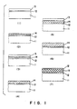
- the porous thin film 13 of gel is converted to a film 14 formed of a crystalline metal oxide.
- the sol prepared above was further spin-coated on the substrate with the thin film formed thereon, and the coating was pre-sintered at 350°C to laminate a 0.4 ⁇ m-thick porous thin film of gel onto the previously formed thin film.
- the laminate was pre-annealed at 550°C for one hr to form a crystalline, dense, thin film.
- the sol prepared above was further spin-coated on the thin film, and the coating was pre-sintered at 350°C to laminate a 0.4 ⁇ m-thick porous thin film of gel onto the above thin film.
- the laminate was then pre-annealed at 550°C for one hr, thereby forming a 0.9 ⁇ m-thick crystalline, dense, thin film.
- the laminate was heated to 650°C over a period of 5 sec in an oxygen atmosphere using an RTA (rapid thermal annealing) oven and held at that temperature for one min, thereby carrying out pre-annealing.
- RTA rapid thermal annealing
- the average grain area of crystal grains observed on the surface of the thin films thus obtained was as given in Table 2. None of the thin films of Examples 10 to 20 suffered from cracking. Further, no interface was observed for the other thin films.
- Amorphous, porous, thin films of gel having thicknesses as shown in Table 3 were formed in the same manner as in Example 1, except that the diluting solvent and the coverage of the sol were varied.
- the thin films of gel were then pre-annealed at 550°C for one hr, thereby preparing crystalline dense films.
- the above procedure was repeated the number of times as specified in Table 3 to laminate films, thereby preparing 2- ⁇ m thick thin films.
- the thin films were annealed at 750°C for one hr under an oxygen stream in an annealing oven to prepare piezoelectric thin films.
- annealing was carried out under an oxygen atmosphere in an RTA oven at temperatures specified in Table 4.
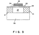
- a groove having a width of 0.3 mm was formed within the silicon wafer by anisotropic etching.
- An upper electrode of gold was then formed on the piezoelectric thin films, and the substrates with the piezoelectric thin films formed thereon were then joined to a second substrate of glass to form ink passages. Head units were taken off from the substrates and used as an ink jet recording head.
- Example 2 The procedure of Example 1 (2) was repeated, except that the thin film prepared in the above step (1) was pre-annealed at 600°C for 30 min and further at 800°C for 30 min instead of the annealing at 700°C for one hr.
- the substrate prepared above was held at 600°C for 30 min and further at 800°C for 30 min to carry out annealing.
- a 0.9 ⁇ m-thick piezoelectric thin film was prepared wherein the average grain area of crystal grains observed on the surface of the film under a metallographic microscope was 0.3 ⁇ m 2 .
- a part of the piezoelectric thin film was dissolved in aqua regia, and the molar ratio of Pb to Zr to Ti in the piezoelectric thin film was determined by ICP and found to be 1 : 0.52 : 0.48 which was the same as the molar ratio of Pb to Zr to Ti in the starting materials.
Landscapes
- Chemical & Material Sciences (AREA)
- Dispersion Chemistry (AREA)
- Engineering & Computer Science (AREA)
- Manufacturing & Machinery (AREA)
- Particle Formation And Scattering Control In Inkjet Printers (AREA)
- Compositions Of Oxide Ceramics (AREA)
Claims (7)
- Procédé de préparation d'une couche piézoélectrique mince par un procédé sol-gel, comprenant les étapes suivantes :a) le revêtement d'un substrat d'une composition de sol comprenant un sol d'un ingrédient métallique destiné à constituer une couche piézoélectrique, et un composé polymère, puis le séchage du revêtement afin qu'il forme une couche,b) le frittage préalable de la couche à une température comprise entre 300 et 450 °C pour la formation d'une couche mince poreuse de gel contenant un oxyde métallique amorphe,c) un recuit préalable de la couche mince poreuse de gel à une température comprise entre 400 et 800 °C afin que la couche soit mise sous forme d'une couche formée d'un oxyde métallique cristallin,d) la répétition des étapes a), b) et c) au moins une fois pour la formation de couches empilées d'un oxyde métallique cristallin, ete) le recuit des couches préparées dans l'étape d) à une température comprise entre 600 et 1 200 °C pour la croissance de grains cristallins de type pérovskite dans la couche à une plus grande dimension.
- Procédé de préparation d'une couche piézoélectrique mince par un procédé sol-gel selon la revendication 1, caractérisé en ce queles étapes (a) et (b) sont répétées au moins une fois pour la formation de couches stratifiées formées de couches minces poreuses avant l'étape c),l'étape c) comprend le recuit préalable des couches ainsi stratifiées de couches minces, etl'étape d) comprend la répétition au moins une fois des étapes répétées a) et b) et de l'étape c).
- Procédé de préparation d'une couche piézoélectrique mince selon la revendication 1 ou 2,
caractérisé en ce que
le recuit de l'étape e) est réalisé à une température comprise entre 800 et 1 000 °C. - Procédé de préparation d'une couche piézoélectrique mince selon la revendication 1 ou 2,
caractérisé en ce que
le recuit préalable de l'étape c) est exécuté en deux phases, la première phase étant exécutée à une température entre 400 et 600 °C et la seconde phase à une température comprise entre 600 et 800 °C. - Procédé de préparation d'une couche piézoélectrique mince selon la revendication 1 ou 2,
caractérisé en ce que
le recuit de l'étape e) est réalisé en deux phases, la première phase étant exécutée à une température comprise entre 600 et 800 °C et la seconde phase à une température comprise entre 800 et 1 000 °C. - Procédé de préparation d'une couche piézoélectrique mince selon la revendication 1 ou 2,
caractérisé en ce que
l'épaisseur de la couche mince poreuse formée dans l'étape b) est comprise entre 0,01 et 1 µm. - Procédé de préparation d'une couche piézoélectrique mince selon la revendication 1 ou 2,
caractérisé en ce que
le stratifié d'oxyde métallique cristallin préparé dans l'étape d) est mis sous forme de motifs constituant un dispositif piézoélectrique à couches minces avant l'étape e).
Applications Claiming Priority (6)
| Application Number | Priority Date | Filing Date | Title |
|---|---|---|---|
| JP31035/95 | 1995-02-20 | ||
| JP3103595 | 1995-02-20 | ||
| JP3103595 | 1995-02-20 | ||
| JP32266295 | 1995-12-12 | ||
| JP322662/95 | 1995-12-12 | ||
| JP32266295 | 1995-12-12 |
Publications (2)
| Publication Number | Publication Date |
|---|---|
| EP0727832A1 EP0727832A1 (fr) | 1996-08-21 |
| EP0727832B1 true EP0727832B1 (fr) | 2001-11-28 |
Family
ID=26369488
Family Applications (1)
| Application Number | Title | Priority Date | Filing Date |
|---|---|---|---|
| EP19960102532 Expired - Lifetime EP0727832B1 (fr) | 1995-02-20 | 1996-02-20 | Procédé de fabrication d'une couche mince piézoélectrique |
Country Status (4)
| Country | Link |
|---|---|
| US (1) | US6543107B1 (fr) |
| EP (1) | EP0727832B1 (fr) |
| JP (1) | JP3405498B2 (fr) |
| DE (1) | DE69617288T2 (fr) |
Cited By (2)
| Publication number | Priority date | Publication date | Assignee | Title |
|---|---|---|---|---|
| DE102007029600A1 (de) * | 2007-06-27 | 2009-01-02 | Siemens Ag | Bleizirkonattitanat mit Scandium-Wolfram-Dotierung, Verfahren zum Herstellen eines piezokeramischen Bauteils unter Verwendung des Bleizirkonattitanats und Verwendung des piezokeramischen Bauteils |
| DE102007029613A1 (de) * | 2007-06-27 | 2009-01-02 | Siemens Ag | Bleizirkonattitanat mit Nickel-Wolfram-Dotierung, Verfahren zum Herstellen eines piezokeramischen Bauteils unter Verwendung des Bleizirkonattitanats und Verwendung des piezokeramischen Bauteils |
Families Citing this family (50)
| Publication number | Priority date | Publication date | Assignee | Title |
|---|---|---|---|---|
| JP3209082B2 (ja) * | 1996-03-06 | 2001-09-17 | セイコーエプソン株式会社 | 圧電体薄膜素子及びその製造方法、並びにこれを用いたインクジェット式記録ヘッド |
| EP0867952B8 (fr) * | 1997-03-27 | 2003-05-28 | Seiko Epson Corporation | Procédé de fabrication d'élément piézoélectrique |
| EP0932210B1 (fr) * | 1998-01-22 | 2007-05-16 | Seiko Epson Corporation | Elément à couche mince piézoélectrique et tête d'enregistrement à jet d'encre en faisant usage |
| US6478412B1 (en) * | 1999-01-22 | 2002-11-12 | Kansai Research Institute | Piezoelectric thin film device, its production method, and ink-jet recording head |
| JP2001203401A (ja) * | 2000-01-18 | 2001-07-27 | Seiko Epson Corp | 圧電体素子及びその製造方法、インクジェット式記録ヘッド並びにインクジェットプリンタ |
| US7527982B1 (en) * | 2000-07-14 | 2009-05-05 | Kabushiki Kaisha Toshiba | Manufacturing method of a semiconductor device including a crystalline insulation film made of perovskite type oxide |
| JP4925516B2 (ja) * | 2001-03-30 | 2012-04-25 | 京セラ株式会社 | 積層型圧電アクチュエータ及び噴射装置 |
| US6730575B2 (en) | 2001-08-30 | 2004-05-04 | Micron Technology, Inc. | Methods of forming perovskite-type material and capacitor dielectric having perovskite-type crystalline structure |
| JP4286492B2 (ja) * | 2002-06-13 | 2009-07-01 | 富士通株式会社 | 強誘電体キャパシタの製造方法 |
| JP3974096B2 (ja) * | 2002-09-20 | 2007-09-12 | キヤノン株式会社 | 圧電体素子及びインクジェット記録ヘッド |
| JP3999156B2 (ja) * | 2003-03-31 | 2007-10-31 | 日本碍子株式会社 | 圧電/電歪膜型素子及び圧電/電歪磁器組成物 |
| EP2365553A1 (fr) * | 2003-07-28 | 2011-09-14 | Kyocera Corporation | Élément piézoélectrique à multicouches |
| JP5013035B2 (ja) | 2003-12-11 | 2012-08-29 | セイコーエプソン株式会社 | 誘電体膜の製造方法及び液体噴射ヘッドの製造方法 |
| US7094709B2 (en) * | 2004-06-15 | 2006-08-22 | Braggone Oy | Method of synthesizing hybrid metal oxide materials and applications thereof |
| US7739777B2 (en) * | 2004-08-31 | 2010-06-22 | Brother Kogyo Kabushiki Kaisha | Method of manufacturing a liquid transporting apparatus |
| JP4868200B2 (ja) * | 2004-09-22 | 2012-02-01 | ブラザー工業株式会社 | 圧電アクチュエータおよびインクジェットヘッドの製造方法 |
| BRPI0519739A2 (pt) * | 2004-12-30 | 2009-03-10 | Cinv Ag | combinaÇço compreendendo um agente fornecendo um sinal, um material de implante e uma droga |
| SI1836239T1 (sl) * | 2005-01-13 | 2009-04-30 | Cinv Ag | Kompozitni materiali, ki vsebujejo ogljikove nanodelce |
| BRPI0606486A2 (pt) * | 2005-01-24 | 2009-06-30 | Cinv Ag | materiais compósitos contendo metal |
| MX2007009430A (es) * | 2005-02-03 | 2007-08-17 | Cinv Ag | Materiales para suministro de farmacos producidos mediante la tecnologia de sol/gel. |
| BRPI0608506A2 (pt) * | 2005-03-18 | 2010-01-05 | Cinv Ag | processo para preparação de materiais metálicos porosos sinterizados |
| JP5019020B2 (ja) | 2005-03-31 | 2012-09-05 | セイコーエプソン株式会社 | 誘電体膜の製造方法及び圧電体素子の製造方法並びに液体噴射ヘッドの製造方法 |
| AU2006265193A1 (en) * | 2005-07-01 | 2007-01-11 | Cinvention Ag | Process for the production of porous reticulated composite materials |
| EA012091B1 (ru) * | 2005-07-01 | 2009-08-28 | Синвеншен Аг | Медицинское устройство, содержащее сетчатый композиционный материал |
| US7673976B2 (en) * | 2005-09-16 | 2010-03-09 | Eastman Kodak Company | Continuous ink jet apparatus and method using a plurality of break-off times |
| US7364276B2 (en) * | 2005-09-16 | 2008-04-29 | Eastman Kodak Company | Continuous ink jet apparatus with integrated drop action devices and control circuitry |
| US7273270B2 (en) | 2005-09-16 | 2007-09-25 | Eastman Kodak Company | Ink jet printing device with improved drop selection control |
| JP5088916B2 (ja) * | 2005-10-28 | 2012-12-05 | 富士フイルム株式会社 | 無機膜基板の製造方法 |
| JP4998675B2 (ja) * | 2006-03-27 | 2012-08-15 | セイコーエプソン株式会社 | 圧電素子の製造方法及び液体噴射ヘッド |
| US7777395B2 (en) * | 2006-10-12 | 2010-08-17 | Eastman Kodak Company | Continuous drop emitter with reduced stimulation crosstalk |
| JP4737027B2 (ja) * | 2006-10-13 | 2011-07-27 | セイコーエプソン株式会社 | 圧電体素子の製造方法、及びインクジェット式記録ヘッドの製造方法 |
| US7879395B2 (en) * | 2006-10-17 | 2011-02-01 | Qimonda Ag | Method of preparing a coating solution and a corresponding use of the coating solution for coating a substrate |
| JP2008205048A (ja) * | 2007-02-16 | 2008-09-04 | Seiko Epson Corp | 圧電素子の製造方法及び液体噴射ヘッドの製造方法 |
| US7758171B2 (en) * | 2007-03-19 | 2010-07-20 | Eastman Kodak Company | Aerodynamic error reduction for liquid drop emitters |
| JP2009054618A (ja) * | 2007-08-23 | 2009-03-12 | Seiko Epson Corp | 圧電素子の製造方法、誘電体層の製造方法、およびアクチュエータの製造方法 |
| JP2008153674A (ja) * | 2007-12-25 | 2008-07-03 | Seiko Epson Corp | インクジェット式記録ヘッド及び圧電体素子 |
| KR101669953B1 (ko) | 2010-03-26 | 2016-11-09 | 삼성전자 주식회사 | 산화물 박막, 산화물 박막의 형성 방법 및 산화물 박막을 포함하는 전자 소자 |
| JP5974485B2 (ja) * | 2011-09-16 | 2016-08-23 | 株式会社リコー | 電気機械変換素子の製造方法 |
| US9168740B2 (en) | 2013-04-11 | 2015-10-27 | Eastman Kodak Company | Printhead including acoustic dampening structure |
| US9162454B2 (en) | 2013-04-11 | 2015-10-20 | Eastman Kodak Company | Printhead including acoustic dampening structure |
| EP3125317B1 (fr) | 2014-03-27 | 2022-04-27 | Mitsubishi Materials Corporation | Composition de formation de film piézoélectrique dopé au mn à base de pzt et film piézoélectrique dopé au mn à base de pzt |
| KR102330630B1 (ko) | 2014-03-28 | 2021-11-23 | 미쓰비시 마테리알 가부시키가이샤 | Mn 및 Nb 도프의 PZT 계 압전체막 형성용 조성물 |
| US20150279671A1 (en) * | 2014-03-28 | 2015-10-01 | Industry-Academic Cooperation Foundation, Yonsei University | Method for forming oxide thin film and method for fabricating oxide thin film transistor employing germanium doping |
| US9199462B1 (en) | 2014-09-19 | 2015-12-01 | Eastman Kodak Company | Printhead with print artifact supressing cavity |
| US20160138182A1 (en) * | 2014-11-18 | 2016-05-19 | Wisconsin Alumni Research Foundation | Methods for forming mixed metal oxide epitaxial films |
| JP6891734B2 (ja) * | 2017-08-29 | 2021-06-18 | セイコーエプソン株式会社 | 圧電素子および液体吐出ヘッド |
| RU2673444C1 (ru) * | 2017-12-19 | 2018-11-26 | Акционерное общество "Научно-исследовательский институт "Элпа" с опытным производством" | Способ получения пористой пьезокерамики с анизотропией диэлектрической проницаемости и ряда других параметров |
| CN113272982B (zh) * | 2018-11-09 | 2024-06-14 | 麦斯卓微电子(南京)有限公司 | 压电致动器制造方法 |
| CN110752286B (zh) * | 2019-10-25 | 2023-04-07 | 业成科技(成都)有限公司 | 压电薄膜及其制备方法和压电薄膜传感器 |
| JP7799269B2 (ja) * | 2021-10-23 | 2026-01-15 | 国立大学法人 熊本大学 | ゾルゲル複合体圧電センサ作成方法 |
Citations (1)
| Publication number | Priority date | Publication date | Assignee | Title |
|---|---|---|---|---|
| EP0691693A1 (fr) * | 1994-07-08 | 1996-01-10 | Seiko Epson Corporation | Dispositif piézo-électrique à couche mince et tête d'enregistrement à jet d'encre comportant ce dispositif |
Family Cites Families (11)
| Publication number | Priority date | Publication date | Assignee | Title |
|---|---|---|---|---|
| US4820586A (en) * | 1980-07-23 | 1989-04-11 | Minnesota Mining And Manufacturing Company | Pyroelectric and isotropic piezoelectric polymer blends |
| US4946710A (en) * | 1987-06-02 | 1990-08-07 | National Semiconductor Corporation | Method for preparing PLZT, PZT and PLT sol-gels and fabricating ferroelectric thin films |
| CA2065381A1 (fr) * | 1989-04-21 | 1990-10-22 | Paul Groves | Procede de fabrication de ceramique en couche mince par transformation sol-gel |
| WO1990013149A1 (fr) * | 1989-04-27 | 1990-11-01 | Queen's University At Kingston | PROCEDE SOL-GEL DE PREPARATION DE MINCES FILMS EN Pb(Zr,Ti)O¿3? |
| US5265315A (en) * | 1990-11-20 | 1993-11-30 | Spectra, Inc. | Method of making a thin-film transducer ink jet head |
| US5500988A (en) * | 1990-11-20 | 1996-03-26 | Spectra, Inc. | Method of making a perovskite thin-film ink jet transducer |
| JPH04259380A (ja) * | 1991-02-13 | 1992-09-14 | Mitsubishi Materials Corp | Pzt強誘電体薄膜の結晶配向性制御方法 |
| US5271956A (en) * | 1991-12-30 | 1993-12-21 | Eastman Kodak Company | Method of forming ternary metal fluoride films by the decomposition of metallo-organic compounds in the presence of a fluorinating agent |
| US5271955A (en) * | 1992-04-06 | 1993-12-21 | Motorola, Inc. | Method for making a semiconductor device having an anhydrous ferroelectric thin film |
| US5683614A (en) * | 1996-08-16 | 1997-11-04 | Sandia Corporation | Sol-gel type synthesis of Bi2 (Sr,Ta2)O9 using an acetate based system |
| US5873154A (en) * | 1996-10-17 | 1999-02-23 | Nokia Mobile Phones Limited | Method for fabricating a resonator having an acoustic mirror |
-
1996
- 1996-02-20 JP JP03234696A patent/JP3405498B2/ja not_active Expired - Fee Related
- 1996-02-20 DE DE69617288T patent/DE69617288T2/de not_active Expired - Lifetime
- 1996-02-20 EP EP19960102532 patent/EP0727832B1/fr not_active Expired - Lifetime
-
1997
- 1997-02-28 US US08/807,724 patent/US6543107B1/en not_active Expired - Fee Related
Patent Citations (1)
| Publication number | Priority date | Publication date | Assignee | Title |
|---|---|---|---|---|
| EP0691693A1 (fr) * | 1994-07-08 | 1996-01-10 | Seiko Epson Corporation | Dispositif piézo-électrique à couche mince et tête d'enregistrement à jet d'encre comportant ce dispositif |
Non-Patent Citations (1)
| Title |
|---|
| M. KLEE ET AL.: "Processing and electrical properties of Pb (ZrxTi1-x)O3 (x=0.2-0.75) films: Comparison of metallo-organic decomposition and sol-gel processes", J. APPL. PHYS., vol. 72, no. 4, 15 August 1992 (1992-08-15), USA, pages 1566 - 1576 * |
Cited By (2)
| Publication number | Priority date | Publication date | Assignee | Title |
|---|---|---|---|---|
| DE102007029600A1 (de) * | 2007-06-27 | 2009-01-02 | Siemens Ag | Bleizirkonattitanat mit Scandium-Wolfram-Dotierung, Verfahren zum Herstellen eines piezokeramischen Bauteils unter Verwendung des Bleizirkonattitanats und Verwendung des piezokeramischen Bauteils |
| DE102007029613A1 (de) * | 2007-06-27 | 2009-01-02 | Siemens Ag | Bleizirkonattitanat mit Nickel-Wolfram-Dotierung, Verfahren zum Herstellen eines piezokeramischen Bauteils unter Verwendung des Bleizirkonattitanats und Verwendung des piezokeramischen Bauteils |
Also Published As
| Publication number | Publication date |
|---|---|
| US6543107B1 (en) | 2003-04-08 |
| JPH09223830A (ja) | 1997-08-26 |
| DE69617288D1 (de) | 2002-01-10 |
| DE69617288T2 (de) | 2002-05-23 |
| EP0727832A1 (fr) | 1996-08-21 |
| JP3405498B2 (ja) | 2003-05-12 |
Similar Documents
| Publication | Publication Date | Title |
|---|---|---|
| US6543107B1 (en) | Method of producing a piezoelectric thin film | |
| US6140746A (en) | Piezoelectric thin film, method for producing the same, and ink jet recording head using the thin film | |
| JP4572346B2 (ja) | 圧電体薄膜素子及びインクジェット式記録ヘッド | |
| JP3520403B2 (ja) | 圧電体薄膜素子、アクチュエータ、インクジェット式記録ヘッド、及びインクジェット式記録装置 | |
| EP2876666B1 (fr) | Procédé de production de film ferroélectrique à couche mince | |
| US5825121A (en) | Thin film piezoelectric device and ink jet recording head comprising the same | |
| US6419849B1 (en) | Method for manufacturing piezoelectric material | |
| EP0794579B1 (fr) | Dispositif à couche mince piézoélectrique | |
| EP2525393B1 (fr) | Procédé de production de film ferroélectrique à couche mince | |
| JPWO1998002378A1 (ja) | 強誘電体素子及びその製造方法 | |
| JP3903474B2 (ja) | アクチュエータ、及びインクジェット式記録ヘッド、並びに圧電体薄膜素子の製造方法 | |
| EP0932210B1 (fr) | Elément à couche mince piézoélectrique et tête d'enregistrement à jet d'encre en faisant usage | |
| JP5370332B2 (ja) | 圧電体素子およびインクジェット式記録ヘッド | |
| JP4144043B2 (ja) | 圧電体薄膜素子の製造方法 | |
| JP4144653B2 (ja) | インクジェット式記録ヘッド |
Legal Events
| Date | Code | Title | Description |
|---|---|---|---|
| PUAI | Public reference made under article 153(3) epc to a published international application that has entered the european phase |
Free format text: ORIGINAL CODE: 0009012 |
|
| AK | Designated contracting states |
Kind code of ref document: A1 Designated state(s): CH DE FR GB IT LI NL SE |
|
| 17P | Request for examination filed |
Effective date: 19960911 |
|
| 17Q | First examination report despatched |
Effective date: 19971205 |
|
| RTI1 | Title (correction) |
Free format text: METHOD OF PRODUCNING A PIEZOELECTRIC THIN FILM |
|
| GRAG | Despatch of communication of intention to grant |
Free format text: ORIGINAL CODE: EPIDOS AGRA |
|
| GRAG | Despatch of communication of intention to grant |
Free format text: ORIGINAL CODE: EPIDOS AGRA |
|
| GRAH | Despatch of communication of intention to grant a patent |
Free format text: ORIGINAL CODE: EPIDOS IGRA |
|
| GRAH | Despatch of communication of intention to grant a patent |
Free format text: ORIGINAL CODE: EPIDOS IGRA |
|
| GRAA | (expected) grant |
Free format text: ORIGINAL CODE: 0009210 |
|
| AK | Designated contracting states |
Kind code of ref document: B1 Designated state(s): CH DE FR GB IT LI NL SE |
|
| REG | Reference to a national code |
Ref country code: CH Ref legal event code: EP |
|
| REG | Reference to a national code |
Ref country code: CH Ref legal event code: NV Representative=s name: PATENTANWAELTE FELDMANN & PARTNER AG |
|
| REG | Reference to a national code |
Ref country code: GB Ref legal event code: IF02 |
|
| REF | Corresponds to: |
Ref document number: 69617288 Country of ref document: DE Date of ref document: 20020110 |
|
| ET | Fr: translation filed | ||
| PLBE | No opposition filed within time limit |
Free format text: ORIGINAL CODE: 0009261 |
|
| STAA | Information on the status of an ep patent application or granted ep patent |
Free format text: STATUS: NO OPPOSITION FILED WITHIN TIME LIMIT |
|
| 26N | No opposition filed | ||
| REG | Reference to a national code |
Ref country code: CH Ref legal event code: PFA Owner name: SEIKO EPSON CORPORATION Free format text: SEIKO EPSON CORPORATION#4-1, NISHISHINJUKU 2-CHOME#SHINJUKU-KU TOKYO-TO (JP) -TRANSFER TO- SEIKO EPSON CORPORATION#4-1, NISHISHINJUKU 2-CHOME#SHINJUKU-KU TOKYO-TO (JP) |
|
| PGFP | Annual fee paid to national office [announced via postgrant information from national office to epo] |
Ref country code: IT Payment date: 20120217 Year of fee payment: 17 |
|
| PGFP | Annual fee paid to national office [announced via postgrant information from national office to epo] |
Ref country code: GB Payment date: 20130220 Year of fee payment: 18 Ref country code: CH Payment date: 20130212 Year of fee payment: 18 Ref country code: DE Payment date: 20130213 Year of fee payment: 18 Ref country code: FR Payment date: 20130301 Year of fee payment: 18 Ref country code: SE Payment date: 20130212 Year of fee payment: 18 |
|
| PGFP | Annual fee paid to national office [announced via postgrant information from national office to epo] |
Ref country code: NL Payment date: 20130216 Year of fee payment: 18 |
|
| REG | Reference to a national code |
Ref country code: DE Ref legal event code: R119 Ref document number: 69617288 Country of ref document: DE |
|
| REG | Reference to a national code |
Ref country code: NL Ref legal event code: V1 Effective date: 20140901 |
|
| REG | Reference to a national code |
Ref country code: CH Ref legal event code: PL Ref country code: SE Ref legal event code: EUG |
|
| GBPC | Gb: european patent ceased through non-payment of renewal fee |
Effective date: 20140220 |
|
| PG25 | Lapsed in a contracting state [announced via postgrant information from national office to epo] |
Ref country code: NL Free format text: LAPSE BECAUSE OF NON-PAYMENT OF DUE FEES Effective date: 20140901 Ref country code: LI Free format text: LAPSE BECAUSE OF NON-PAYMENT OF DUE FEES Effective date: 20140228 Ref country code: CH Free format text: LAPSE BECAUSE OF NON-PAYMENT OF DUE FEES Effective date: 20140228 |
|
| REG | Reference to a national code |
Ref country code: DE Ref legal event code: R079 Ref document number: 69617288 Country of ref document: DE Free format text: PREVIOUS MAIN CLASS: H01L0041240000 Ipc: H01L0041318000 |
|
| REG | Reference to a national code |
Ref country code: FR Ref legal event code: ST Effective date: 20141031 |
|
| PG25 | Lapsed in a contracting state [announced via postgrant information from national office to epo] |
Ref country code: SE Free format text: LAPSE BECAUSE OF NON-PAYMENT OF DUE FEES Effective date: 20140221 |
|
| REG | Reference to a national code |
Ref country code: DE Ref legal event code: R119 Ref document number: 69617288 Country of ref document: DE Effective date: 20140902 Ref country code: DE Ref legal event code: R079 Ref document number: 69617288 Country of ref document: DE Free format text: PREVIOUS MAIN CLASS: H01L0041240000 Ipc: H01L0041318000 Effective date: 20141105 |
|
| PG25 | Lapsed in a contracting state [announced via postgrant information from national office to epo] |
Ref country code: DE Free format text: LAPSE BECAUSE OF NON-PAYMENT OF DUE FEES Effective date: 20140902 Ref country code: GB Free format text: LAPSE BECAUSE OF NON-PAYMENT OF DUE FEES Effective date: 20140220 Ref country code: FR Free format text: LAPSE BECAUSE OF NON-PAYMENT OF DUE FEES Effective date: 20140228 |
|
| PG25 | Lapsed in a contracting state [announced via postgrant information from national office to epo] |
Ref country code: IT Free format text: LAPSE BECAUSE OF NON-PAYMENT OF DUE FEES Effective date: 20140220 |