EP0729228A1 - Cellule de base pour filtre analogique programmable à temps continu - Google Patents
Cellule de base pour filtre analogique programmable à temps continu Download PDFInfo
- Publication number
- EP0729228A1 EP0729228A1 EP95830049A EP95830049A EP0729228A1 EP 0729228 A1 EP0729228 A1 EP 0729228A1 EP 95830049 A EP95830049 A EP 95830049A EP 95830049 A EP95830049 A EP 95830049A EP 0729228 A1 EP0729228 A1 EP 0729228A1
- Authority
- EP
- European Patent Office
- Prior art keywords
- cell
- accordance
- stage
- analog
- cells
- Prior art date
- Legal status (The legal status is an assumption and is not a legal conclusion. Google has not performed a legal analysis and makes no representation as to the accuracy of the status listed.)
- Granted
Links
Images

Classifications
-
- H—ELECTRICITY
- H03—ELECTRONIC CIRCUITRY
- H03H—IMPEDANCE NETWORKS, e.g. RESONANT CIRCUITS; RESONATORS
- H03H15/00—Transversal filters
-
- H—ELECTRICITY
- H03—ELECTRONIC CIRCUITRY
- H03H—IMPEDANCE NETWORKS, e.g. RESONANT CIRCUITS; RESONATORS
- H03H11/00—Networks using active elements
- H03H11/02—Multiple-port networks
- H03H11/04—Frequency selective two-port networks
- H03H11/0422—Frequency selective two-port networks using transconductance amplifiers, e.g. gmC filters
Definitions
- the present invention relates to an elementary cell structure for programmable time-continuous analog filters and in particular for read/write operations on magnetic supports.
- the present invention relates to a cell comprising an amplifier stage inserted between a first reference supply voltage and a second reference voltage having a first and a second input terminals and an output terminal.
- the present invention also relates to a transverse analog filter and a delay chain provided by means of a series of cells of the above type.
- the signals must be processed in an appropriate manner to avoid data reading and memorization errors.
- an analog signal picked up e.g. by a read/write head of the magnetic support is processed and reconstructed in digital format by means of an equalizing device.
- the analog signal is first subjected to an analog equalization by means of a variable-gain input amplifier and successively processed through a time-continuous low-pass analog filter.
- the majority of analog filters can be manufactured starting from low-pass elementary cells.
- FIR Finite Impulse Response
- each of the elementary cells making up a FIR filter has a transfer function to supply at the output the input signal delayed according to a predetermined value, called unit delay.
- the delay with which the input signal appears at the output is a function of the signal frequency. More specifically the delay is the derivative in relation to the frequency with changed sign of the transfer function phase between the input and the output.
- the technical problem underlying the present invention is to conceive an elementary cell structure of the analog type to provide time-continuous filters having structural and functional characteristics allowing replacing digital filters which still limit the use of the PRML technique in read/write devices provided in accordance with the prior art.
- Another purpose of the present invention is to conceive a delay line achieved with a chain of elementary cells allowing introduction in the filtering phase of a delay of any predetermined value without thereby distorting the input signal either in phase or in amplitude.
- the solution idea underlying the present invention is to provide a symmetrical structure of the time-continuous analog type comprising two identical half-cells provided starting from a transconductance amplifier stage.
- transverse analog filter comprising a plurality of elementary cells in accordance with claim 1 and following.
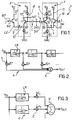
- reference number 1 indicates as a whole and schematically an elementary analog cell structure provided in accordance with the present invention.
- This structure is designed in particular but not exclusively for the manufacture of programmable time-continuous analog filters for read/write operations on magnetic supports.
- the cell 1 comprises essentially two identical half-cells 2 and 2' inserted between a first reference supply voltage Vcc and a second reference voltage, e.g. a signal ground GND.
- the first half-cell 2 comprises a transconductance amplifier stage 3 with an input terminal IN1 and an output terminal OUT.
- the amplifier stage 3 comprises a pair of transistors T1 and T2 having their emitter terminals E1 and E2 respectively connected together and, through a bias current generator G1, to the second reference voltage GND.
- the transistors T1 and T2 are, in the preferred embodiment shown here in FIG. 1, type NPN BJT bipolar transistors.
- the cell 1 in accordance with the present invention could also be provided by means of type PNP bipolar transistors or by means of field effect MOS transistors either of the NMOS or the PMOS type.
- the transistor T1 has its collector terminal C1 connected to the reference supply voltage Vcc while the base terminal B1 of the same transistor T1 coincides with the input terminal IN1 of the amplifier stage 3.
- the transistor T2 has its base terminal B2 and collector terminal C2 short-circuited together in an essentially diode configuration.
- the collector terminal C2 coincides with the output terminal OUT of the amplifier stage 3 and is connected to the reference supply voltage Vcc by means of a second generator G2 of bias current Ib.
- the first generator G1 delivers a bias current 2*Ib double that delivered by the second generator G2.
- the base - or control - terminal B2 of the transistor T2 is connected to a circuit node X for connection between the two half-cells 2 and 2' through a capacitor C.
- the circuit node X can be connected to the second reference voltage GND or can be floating.
- the structure of the second half-cell 2' is fully identical to and symmetrical with that of the first half-cell 2 described above. Therefore, for the sake of simplicity, a detailed description thereof is omitted only noting that all the elements corresponding to those of the first cell 2 are indicated in the figures with the same reference numbers and symbols but with the addition of a superscript.
- the first half-cell 2 and the second half-cell 2' are connected together in the circuit node X.
- the input terminal IN1 of the amplifier stage 3 of the first half-cell 2 coincides with the first input terminal I of the cell 1 as a whole while the input terminal IN1' of the amplifier stage 3' of the second half-cell 2' coincides with the second input terminal I' of the cell 1.
- the output terminals OUT and OUT' of the amplifier stages 3 and 3' are the output terminals O and O' of the cell 1.
- the cell 1 of FIG. 1 is illustrated in a fully differential configuration which has better rejection to common mode signals and noise from the power supply. For the cell 1 it is possible to provide a single-ended configuration.
- an elementary low-pass cell is a circuit structure capable of providing a transfer function between its input and output terminals since it has essentially a single dominant pole at high frequencies.
- the cell 1 can thus be considered as a constant delay element ⁇ c , also equal to 1/2* ⁇ *f c , where f c is the cut-off frequency of the cell 1.
- This delay ⁇ c is however linked to the band of frequencies of the input signal V in , which must not have any component in frequency greater than f c /10 to not have distortion of the output signal V out .
- a delay line LR by means of a cascade of cells 1. Specifically, it is sufficient to connect in parallel the outputs OUT and OUT' of a cell with the inputs I, I' of another cell to obtain a delay line LR consisting of two base cells. It is clear that the base structure can be repeated depending on necessities by connecting in cascade together a number n of cells 1.
- the resulting line LR has a delay equal to n* ⁇ c , i.e. a cut-off frequency f c equal to n* fmaxi , where n is the number of cells 1 cascaded.
- connection in cascade of only five cells 1 is acceptable so as to gain in terms of dispersed power.
- the delay line LR complies with the requirement for having a relatively flat delay but can introduce elements which are not ideal as concerns the frequency response of the output signal.
- the line LR attenuates the high frequency components of the input signal V in .
- FIG. 2 A first example of a FIR transverse filter 4 is shown schematically in FIG. 2.
- the filter 4 comprises a cascade of identical delay lines LR connected through multiplier nodes 5 to a final summation node 6.
- the signal Vo output by the node 6 is obtained by means of a transfer function determined from formula (1) with a unitary delay equal to the delay of the line LR.
- the coefficients a 1 ,..., a n are input at the multiplier nodes 5.
- FIG. 3 shows schematically a second possible embodiment of a filter 4' of the transverse FIR type.
- the filter 4' comprises an summation node 6' to which lead a plurality of delay lines LR' each of which is connected to the summation node 6' through a multiplier node 5'.
- Each of the n delay lines LR' supplies at output a signal delayed n times which is multiplied in each of the nodes 5' by the relative coefficient a 1 ,..., a n in such a manner as to obtain a transfer function in accordance with formula (1).
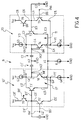
- FIG. 4 is proposed a second embodiment of an elementary analog cell 7 in accordance with the present invention.
- the cell 7 comprises an input stage 8 and an output stage 9.
- the structure of the output stage 9 is shown schematically in FIG. 5.
- the input stage 8 comprises two identical input half-stages 10 and 10' inserted between a first reference supply voltage Vcc and a second reference voltage, e.g. a signal ground GND.
- the first input half-stage 10 comprises a transconductance amplifier stage 11, an input terminal IN4 and an intermediate output terminal OUT1.
- the transconductance amplifier stage 11 comprises a pair of transistors T4 and T5 whose emitter terminals E4 and E5 are connected together to form a first circuit node Y1.
- the circuit node Y1 is connected to the second reference voltage GND through a second bias current generator G4 while the base terminal B5 of the transistor T5 coincides with the input terminal IN4 of the half-stage 10.
- the transistor T4 has its base terminal B4 and collector terminal C4 short-circuited together and to a circuit node Y3.
- the collector C4 coincides with the intermediate output terminal OUT1 of the input half-stage 10.
- the circuit node Y3 is connected through a first generator G3 of bias current 2*Ib to the reference supply voltage Vcc.
- the second generator G4 delivers a bias current 2*Ib identical to that delivered by the first generator G3.
- a third transistor T3 having its own base terminal B3 connected to the collector C5 of the transistor T5 and the emitter terminal E3 connected to a first circuit node X1 common to the two half-stages 10 and 10'.
- the common circuit node X1 is connected to the second reference voltage GND through a common generator G of bias current 2*Ib.
- the value of this generator G is equal to that of the generators G3 and G4.
- the terminal OUT1 is connected to a second circuit node X2 common to the two half-stages 10 and 11 through a first capacitor C 1 .
- the common circuit node X2 is also connected to the second reference voltage GND or may remain floating.
- the input half-stage 10 comprises additionally a bias transistor T6 inserted between the first reference supply voltage Vcc and the collector C5 of the transistor T5.
- This collector C5 is advantageously connected to the second reference voltage GND through a second capacitor C 2 .
- the structure of the second half-stage 11 is fully identical to and symmetrical with that of the first half-stage 10 described above. Therefore, for the sake of brevity, a detailed description thereof is omitted with the note that all the elements corresponding to those of the first half-stage 10 are indicated in FIG. 4 by the same reference numbers and symbols but with the addition of a superscript.
- the output stage 9 has two intermediate input terminals IN5 and IN5' and two final output terminals OUT2 and OUT2'.
- the intermediate output terminals OUT1 and OUT1' of the input stage 8 are connected to the intermediate input terminals IN5 and IN5' of the output stage 9.
- the output stage 9 comprises two identical output half-stages 12 and 12' inserted between the first reference supply voltage Vcc and the second reference voltage GND.
- the half-stage 12 comprises a transistor T7 having its base - or control - terminal B7 coinciding with the input IN5.
- the collector terminal C7 of the transistor T7 is connected to the first reference supply voltage Vcc.
- the emitter terminal E7 of the transistor T7 is connected towards the second reference voltage GND through a bias current generator G6.
- the half-stage 12 comprises in addition a diode D inserted between the final output terminal OUT2 and the emitter E7.
- the final output terminal OUT2 is also connected to the first reference voltage Vcc through a generator G5 of bias current 2*Ib.
- the generator G5 delivers a bias current 2*Ib equal to that delivered by the first generator G3 and the second generator G4 and by the common generator G.
- the generator G6 delivers a bias current 4*Ib which is double than the bias current delivered by the generator G5.
- the final output terminal OUT2 is connected at a common circuit node X3 to the two half-stages 12 and 12' through a capacitor C 3 .
- the node X3 is connected to the second reference voltage GND.
- the structure of the second half-stage 12' is fully identical to and symmetrical with that of the first half-stage 12 described above. Therefore a detailed description thereof is omitted with the only notice that all the elements corresponding to those of the first half-stage 12 are indicated in FIG. 5 by the same reference numbers and symbols but with the addition of a superscript.
- a parallel can be drawn between the structure of the cell 7 as a whole as shown in FIGS. 4 and 5 and the structure of the more compact cell 1 of FIG. 1 considering that the input terminal IN4 of the half-stage 10 corresponds to the first input terminal I of the cell 1 while the second input terminal IN4' of the half-stage 10' corresponds to the second input terminal I' of the cell 1.
- the final output terminals OUT2 and OUT2' of the output stage 9 correspond to the output terminals OUT and OUT' of the cell 1.
- the transfer function FdT' given by formula (8) exhibits a zero on the left which permits partial compensation of the phase effect introduced by the left-hand poles.
- the effect of a zero on the left is to delete a pole on the left.
- the cell 7 of FIGS. 4 and 5 is illustrated in a configuration of the fully differential type offering better rejection to common mode signals and noise from the power supply.
- this cell 7 it is also possible to provide a "single ended" type configuration.
- transistors T3, T4, T5, T6 and T7 are described as type NPN BJT bipolar transistors.
- the cell 7 in accordance with the present invention could however be provided by means of type PNP BJT bipolar transistors or field effect MOS transistors of either the NMOS type or the PMOS type.
Landscapes
- Networks Using Active Elements (AREA)
- Filters That Use Time-Delay Elements (AREA)
- Error Detection And Correction (AREA)
Priority Applications (4)
| Application Number | Priority Date | Filing Date | Title |
|---|---|---|---|
| DE69529397T DE69529397D1 (de) | 1995-02-22 | 1995-02-22 | Basiszelle für ein analoges programmierbares zeitkontinuierliches Filter |
| EP19950830049 EP0729228B1 (fr) | 1995-02-22 | 1995-02-22 | Cellule de base pour filtre analogique programmable à temps continu |
| JP3478396A JPH08288794A (ja) | 1995-02-22 | 1996-02-22 | 基本セル構造、時系列遅延線および直交時系列フィルタ |
| US08/999,962 US6359503B1 (en) | 1995-02-22 | 1997-08-12 | Basic cell for programmable analog time-continuous filter |
Applications Claiming Priority (1)
| Application Number | Priority Date | Filing Date | Title |
|---|---|---|---|
| EP19950830049 EP0729228B1 (fr) | 1995-02-22 | 1995-02-22 | Cellule de base pour filtre analogique programmable à temps continu |
Publications (2)
| Publication Number | Publication Date |
|---|---|
| EP0729228A1 true EP0729228A1 (fr) | 1996-08-28 |
| EP0729228B1 EP0729228B1 (fr) | 2003-01-15 |
Family
ID=8221854
Family Applications (1)
| Application Number | Title | Priority Date | Filing Date |
|---|---|---|---|
| EP19950830049 Expired - Lifetime EP0729228B1 (fr) | 1995-02-22 | 1995-02-22 | Cellule de base pour filtre analogique programmable à temps continu |
Country Status (3)
| Country | Link |
|---|---|
| EP (1) | EP0729228B1 (fr) |
| JP (1) | JPH08288794A (fr) |
| DE (1) | DE69529397D1 (fr) |
Cited By (3)
| Publication number | Priority date | Publication date | Assignee | Title |
|---|---|---|---|---|
| EP0942525A1 (fr) * | 1998-03-13 | 1999-09-15 | Lucent Technologies Inc. | Alignement automatique partagé de la linéarisation, de l' égalisation et du retard dans un amplificateur de puissance à large bande |
| US6154093A (en) * | 1998-04-01 | 2000-11-28 | Lucent Technologies Inc. | Fast adaptive wideband power amplifier feed forward linearizer using a RLS parameter tracking algorithm |
| EP1146639A3 (fr) * | 2000-02-29 | 2003-04-16 | STMicroelectronics S.r.l. | Structure de circuit à réaction anticipée avec zéros programmables, en particulier pour la synthèse de filtres à temps continu |
Citations (2)
| Publication number | Priority date | Publication date | Assignee | Title |
|---|---|---|---|---|
| EP0260785A2 (fr) * | 1986-09-19 | 1988-03-23 | Tektronix, Inc. | Amplificateur à récupération rapide |
| DE3939906A1 (de) * | 1989-12-02 | 1991-06-06 | Rohde & Schwarz | Frequenzfilter ersten oder hoeheren grades |
-
1995
- 1995-02-22 EP EP19950830049 patent/EP0729228B1/fr not_active Expired - Lifetime
- 1995-02-22 DE DE69529397T patent/DE69529397D1/de not_active Expired - Lifetime
-
1996
- 1996-02-22 JP JP3478396A patent/JPH08288794A/ja active Pending
Patent Citations (2)
| Publication number | Priority date | Publication date | Assignee | Title |
|---|---|---|---|---|
| EP0260785A2 (fr) * | 1986-09-19 | 1988-03-23 | Tektronix, Inc. | Amplificateur à récupération rapide |
| DE3939906A1 (de) * | 1989-12-02 | 1991-06-06 | Rohde & Schwarz | Frequenzfilter ersten oder hoeheren grades |
Cited By (4)
| Publication number | Priority date | Publication date | Assignee | Title |
|---|---|---|---|---|
| EP0942525A1 (fr) * | 1998-03-13 | 1999-09-15 | Lucent Technologies Inc. | Alignement automatique partagé de la linéarisation, de l' égalisation et du retard dans un amplificateur de puissance à large bande |
| US6172565B1 (en) | 1998-03-13 | 2001-01-09 | Lucent Technologies Inc. | Adaptive joint linearization, equalization and delay alignment for a wideband power amplifier |
| US6154093A (en) * | 1998-04-01 | 2000-11-28 | Lucent Technologies Inc. | Fast adaptive wideband power amplifier feed forward linearizer using a RLS parameter tracking algorithm |
| EP1146639A3 (fr) * | 2000-02-29 | 2003-04-16 | STMicroelectronics S.r.l. | Structure de circuit à réaction anticipée avec zéros programmables, en particulier pour la synthèse de filtres à temps continu |
Also Published As
| Publication number | Publication date |
|---|---|
| EP0729228B1 (fr) | 2003-01-15 |
| JPH08288794A (ja) | 1996-11-01 |
| DE69529397D1 (de) | 2003-02-20 |
Similar Documents
| Publication | Publication Date | Title |
|---|---|---|
| US4574250A (en) | Switched capacitor filter utilizing a differential input and output circuit and method | |
| US4633223A (en) | DC offset correction circuit utilizing switched capacitor differential integrator | |
| US4633425A (en) | Switched capacitor filter utilizing a differential input and output circuit | |
| US5729230A (en) | Delta-Sigma Δ-Σ modulator having a dynamically tunable continuous time Gm-C architecture | |
| US4769612A (en) | Integrated switched-capacitor filter with improved frequency characteristics | |
| CN106982035A (zh) | 一种低噪声放大器电路 | |
| US20030052738A1 (en) | Semiconductor integrated circuit | |
| US6975171B2 (en) | Balanced amplifier and filter using the same | |
| US6359503B1 (en) | Basic cell for programmable analog time-continuous filter | |
| US4599573A (en) | Switched capacitor filter utilizing a differential input and output circuit and method | |
| US20050114428A1 (en) | Analog delay elements | |
| EP0020131B1 (fr) | Filtre à condensateurs commutés | |
| US3986133A (en) | Wide-band transistor amplifier | |
| EP0729228B1 (fr) | Cellule de base pour filtre analogique programmable à temps continu | |
| JPH01135131A (ja) | 可変等化方式 | |
| EP0744829B1 (fr) | Un filtre passe-haut, notamment pour l'élimination du signal offset dans une chaíne d'amplificateurs | |
| JP2790278B2 (ja) | 遅延回路 | |
| Quinn et al. | A 10.7-MHz CMOS SC radio IF filter using orthogonal hardware modulation | |
| JPH0237723B2 (fr) | ||
| EP1811662B1 (fr) | Filtre biquad passe-bas à gain variable | |
| Wyszynski et al. | Frequency and phase tuning of continuous-time integrated filters using common-mode signals | |
| JP2962694B2 (ja) | D/a変換器用出力回路 | |
| EP0696846B1 (fr) | Structure de filtre passe-haute à zéros programmables | |
| Baschirotto et al. | A high-selectivity switched-capacitor bandpass filter | |
| EP1014573A1 (fr) | Structure de filtrage passe-bas avec égalisation analogue |
Legal Events
| Date | Code | Title | Description |
|---|---|---|---|
| PUAI | Public reference made under article 153(3) epc to a published international application that has entered the european phase |
Free format text: ORIGINAL CODE: 0009012 |
|
| AK | Designated contracting states |
Kind code of ref document: A1 Designated state(s): DE FR GB IT |
|
| 17P | Request for examination filed |
Effective date: 19970228 |
|
| RAP3 | Party data changed (applicant data changed or rights of an application transferred) |
Owner name: STMICROELECTRONICS S.R.L. |
|
| 17Q | First examination report despatched |
Effective date: 20000529 |
|
| GRAG | Despatch of communication of intention to grant |
Free format text: ORIGINAL CODE: EPIDOS AGRA |
|
| GRAG | Despatch of communication of intention to grant |
Free format text: ORIGINAL CODE: EPIDOS AGRA |
|
| GRAH | Despatch of communication of intention to grant a patent |
Free format text: ORIGINAL CODE: EPIDOS IGRA |
|
| GRAH | Despatch of communication of intention to grant a patent |
Free format text: ORIGINAL CODE: EPIDOS IGRA |
|
| GRAA | (expected) grant |
Free format text: ORIGINAL CODE: 0009210 |
|
| AK | Designated contracting states |
Kind code of ref document: B1 Designated state(s): DE FR GB IT |
|
| PG25 | Lapsed in a contracting state [announced via postgrant information from national office to epo] |
Ref country code: FR Free format text: LAPSE BECAUSE OF NON-PAYMENT OF DUE FEES Effective date: 20030115 |
|
| REG | Reference to a national code |
Ref country code: GB Ref legal event code: FG4D |
|
| REF | Corresponds to: |
Ref document number: 69529397 Country of ref document: DE Date of ref document: 20030220 Kind code of ref document: P |
|
| PG25 | Lapsed in a contracting state [announced via postgrant information from national office to epo] |
Ref country code: DE Free format text: LAPSE BECAUSE OF FAILURE TO SUBMIT A TRANSLATION OF THE DESCRIPTION OR TO PAY THE FEE WITHIN THE PRESCRIBED TIME-LIMIT Effective date: 20030416 |
|
| PLBE | No opposition filed within time limit |
Free format text: ORIGINAL CODE: 0009261 |
|
| EN | Fr: translation not filed | ||
| 26N | No opposition filed |
Effective date: 20031016 |
|
| PG25 | Lapsed in a contracting state [announced via postgrant information from national office to epo] |
Ref country code: IT Free format text: LAPSE BECAUSE OF NON-PAYMENT OF DUE FEES;WARNING: LAPSES OF ITALIAN PATENTS WITH EFFECTIVE DATE BEFORE 2007 MAY HAVE OCCURRED AT ANY TIME BEFORE 2007. THE CORRECT EFFECTIVE DATE MAY BE DIFFERENT FROM THE ONE RECORDED. Effective date: 20050222 |
|
| PGFP | Annual fee paid to national office [announced via postgrant information from national office to epo] |
Ref country code: GB Payment date: 20060126 Year of fee payment: 12 |
|
| GBPC | Gb: european patent ceased through non-payment of renewal fee |
Effective date: 20070222 |
|
| PG25 | Lapsed in a contracting state [announced via postgrant information from national office to epo] |
Ref country code: GB Free format text: LAPSE BECAUSE OF NON-PAYMENT OF DUE FEES Effective date: 20070222 |